MPSA92High-voltage PNP transistor
Control a load from its positive rail.
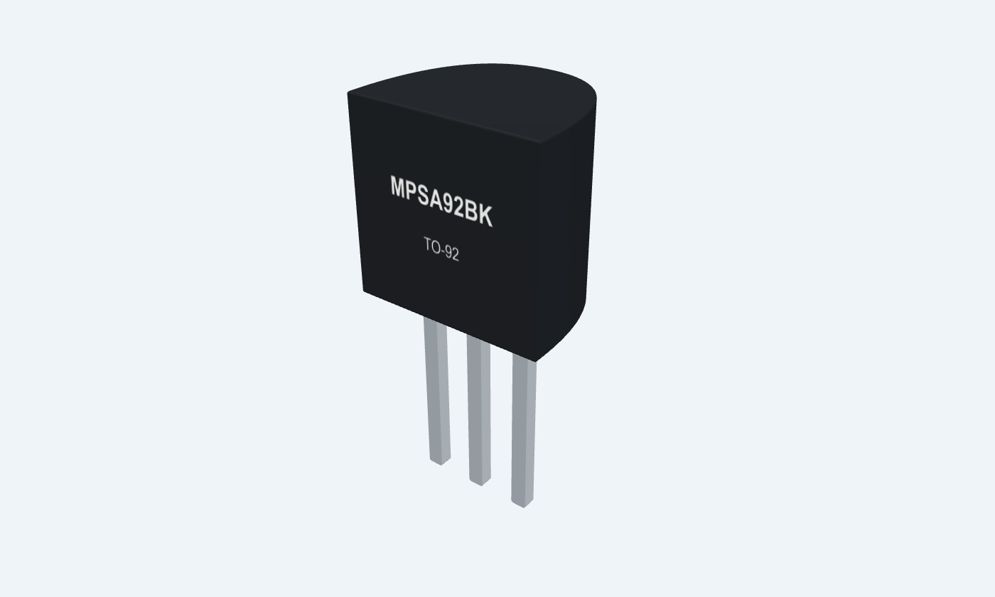
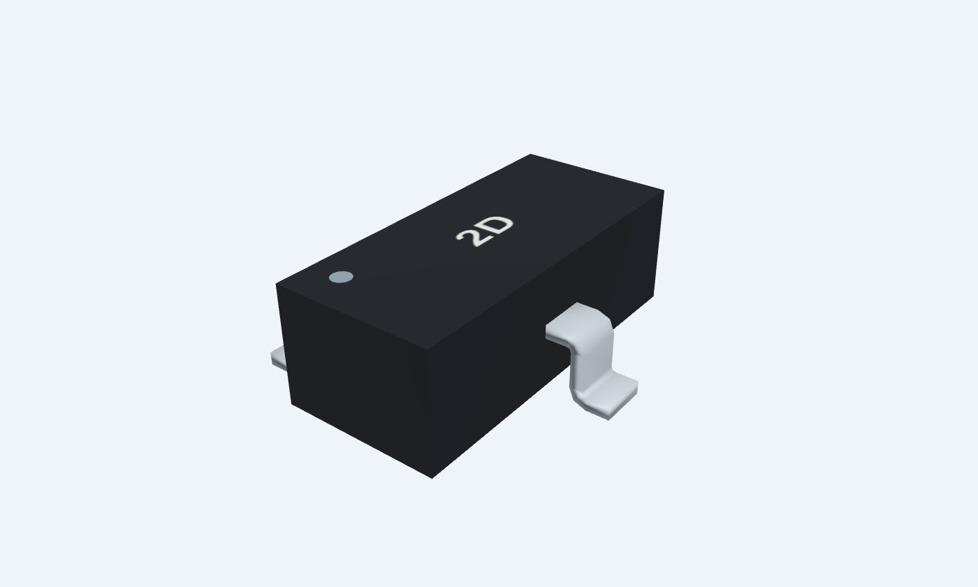
MPSA92 is a PNP bipolar transistor with a 300 V collector-emitter absolute rating and a 500 mA collector-current limit. These are separate stress limits. Dissipation and the operating point constrain how much voltage and current it can handle together. This reference selects Diotec MPSA92BK in the straight-lead TO-92 package: emitter 1, base 2 and collector 3 from the flat front. The separately rated MMBTA92 SMD alternative uses base 1, emitter 2 and collector 3. The pinout, physical package and footprint follow the selected part. The illustrated circuit deliberately uses only 5 V and a small LED load to explain base drive. Its calculated readings do not demonstrate high-voltage operation. High-voltage designs need their own clearance, insulation, transient and thermal review; the footprint alone does not provide that rating.

3Physical pins
MPSA92BKTO-92
Manufacturer-referencedDiotec Semiconductor
Pin diagram
Select a pin to explore its connection
Highlight
MPSA92BKTO-92Front view · flat face · E1, B2, C3
MMBTA92SOT-23Top view · rotated 90° · B1 upper left, E2 lower left, C3 right
Click a lead or use the arrow keys. Front view · flat face · E1, B2, C3
PIN 1 · Supply
EmitterE
Function
Emitter terminal of the bipolar transistor.
How to connect
Connect to +5 V in the high-side example.
Electrical note
TO-92 pin 1 becomes SOT-23 pin 2.
PIN 2 · Base / control
BaseB
Function
Base current controls the collector current within the circuit operating region.
How to connect
Pull down through 4.7 kΩ to turn on; 100 kΩ returns base to emitter.
Electrical note
TO-92 pin 2 becomes SOT-23 pin 1.
PIN 3 · Collector / load
CollectorC
Function
Load-current terminal of the transistor.
How to connect
Feeds the resistor and LED to ground.
Electrical note
Collector remains physical pin 3 in both selected packages.
Key specifications
TO-92 uses E1–B2–C3. SOT-23 uses B1–E2–C3. Check the selected part and mounting conditions before using its limits.
Collector-emitter limit300 V magnitude · absolute
Collector current limit500 mA magnitude · thermal limits apply
TO-92 gain at 10 mA≥40 |VCE| = 10 V
Junction limit150 °C · absolute maximum
Package details
MPSA92BK · TO-92
| Property | Details |
|---|---|
| Manufacturer | Diotec Semiconductor |
| Part number | MPSA92BK |
| Package | TO-92 |
| Connections | 3 pins |
| Mounting | Through-hole |
| Lead pitch | 1.27 mm · straight leads |
| Package code | straight |
| Thermal reference | 625 mW with leads held at ambient temperature 2 mm from case; derate. |
Packages and terminal functions
Reviewed Diotec selections
Manufacturer specifications 4 parameters
Scroll sideways to see all columns.
| Parameter | Value | Conditions / notes |
|---|---|---|
| Through-hole selection | MPSA92BK | Straight-lead TO-92: E1, B2, C3 |
| SMD selection | MMBTA92 | SOT-23: B1, E2, C3 |
| SMD marking | 2D | Manufacturer marking code |
| Polarity | PNP | Magnitudes shown for PNP values |
No specifications match. Try a parameter name or a unit.
Physical pin numbers change between packages; connect by E/B/C function.
TO-92 absolute limits
25°C unless stated
Manufacturer specifications 6 parameters
Scroll sideways to see all columns.
| Parameter | Value | Conditions / notes |
|---|---|---|
| Collector-emitter / collector-base | 300 / 300 V magnitudes | Base open / emitter open |
| Emitter-base reverse | 5 V magnitude | Collector open |
| DC collector current | 500 mA magnitude | Apply power and junction-temperature limits |
| Power dissipation | 625 mW | Leads held at ambient temperature 2 mm from case |
| Junction temperature | −55 to +150°C | Absolute range |
| Junction-to-ambient | <200 K/W | Manufacturer lead-cooling condition |
No specifications match. Try a parameter name or a unit.
300 V and 500 mA are not a simultaneous operating point.
TO-92 electrical characteristics
25°C · package-specific test points
Manufacturer specifications 7 parameters
Scroll sideways to see all columns.
| Parameter | Value | Conditions / notes |
|---|---|---|
| Gain at 1 / 10 / 30 mA | ≥25 / ≥40 / ≥25 | |VCE| = 10 V |
| Collector saturation voltage | ≤0.50 V | |IC| = 20 mA; |IB| = 2 mA |
| Base saturation voltage | ≤0.90 V | |IC| = 20 mA; |IB| = 2 mA |
| Collector-base leakage | ≤250 nA | |VCB| = 200 V; emitter open |
| Emitter-base leakage | ≤100 nA | |VEB| = 3 V; see manufacturer terminal-bias condition |
| Transition frequency | 70 MHz typical | |VCE| = 20 V; |IC| = 10 mA; f = 100 MHz |
| Collector-base capacitance | ≤7 pF | |VCB| = 20 V; 1 MHz |
No specifications match. Try a parameter name or a unit.
On-state values use pulsed measurements; typical frequency is not a guaranteed switching rate.
SMD · MMBTA92
Independent manufacturer reference
Manufacturer specifications 10 parameters
Scroll sideways to see all columns.
| Parameter | Value | Conditions / notes |
|---|---|---|
| VCEO / VCBO / VEBO | 300 / 300 / 6 V magnitudes | Absolute limits with the specified third terminal open |
| DC collector current | 500 mA magnitude | Apply thermal constraints |
| Power dissipation | 250 mW | PCB with 3 mm² copper at each terminal |
| Gain at 10 mA | 80–200 | |VCE| = 10 V |
| Gain at 1 / 30 mA | >25 / >40 | |VCE| = 10 V |
| VCE(sat) / VBE(sat) | <0.50 / <0.90 V | |IC| = 20 mA; |IB| = 2 mA |
| Transition frequency | >50 MHz | |VCE| = 20 V; |IC| = 10 mA; f = 100 MHz |
| Collector-base capacitance | <3 pF | |VCB| = 20 V; 1 MHz |
| Junction / storage | −55 to +150°C | Absolute ranges |
| Body / full lead span | 2.9 × 1.3 / 2.4 mm nominal | Paired-contact pitch 1.9 mm |
No specifications match. Try a parameter name or a unit.
SMD values belong to the exact listed part; do not substitute the axial thermal rating.
TO-92 mechanical reference
Manufacturer straight-lead drawing
Manufacturer specifications 6 parameters
Scroll sideways to see all columns.
| Parameter | Value | Conditions / notes |
|---|---|---|
| Body width / height | 4.6 ±0.1 / 4.6 ±0.1 mm | Black flat-front molded body |
| Body depth | 3.6 ±0.1 mm | Flat face 1.1 ±0.2 mm from lead plane |
| Lead pitch | 1.27 ±0.1 mm | Straight-lead option |
| Lead width / thickness | 0.4 +0.15/−0.05 / 0.34 ±0.05 mm | Silver plated stamped contacts |
| Supplied lead length | ≥12.5 mm | Preview shows trimmed leads for readability |
| Authored pad / hole | 1.10 × 1.55 / 0.80 mm | Engineering footprint; review fabrication tolerance |
No specifications match. Try a parameter name or a unit.
The 2.54 mm formed tape option is a different mounting geometry.
5 V LED example
Teaching assumptions, not measured values
Manufacturer specifications 7 parameters
Scroll sideways to see all columns.
| Parameter | Value | Conditions / notes |
|---|---|---|
| Load / base / bias resistors | 470 Ω / 4.7 kΩ / 100 kΩ | Use separate current limits |
| Assumed drops | LED 2.0 V; |VBE| 0.7 V; |VCE(sat)| 0.2 V | Actual drops vary |
| Collector current | 5.96 mA | (5 − 2 − 0.2) / 470 |
| Net base current | 0.908 mA | (5 − 0.7) / 4700 − 0.7 / 100000 |
| Forced current ratio | Approximately 6.56 | Collector / base current |
| Transistor dissipation | Approximately 1.83 mW | Collector-emitter plus base-emitter terms |
| Inductive loads | Require a revised circuit | Add suitable flyback protection; not pictured here |
No specifications match. Try a parameter name or a unit.
The example is a low-current LED switch; it does not demonstrate the maximum-current rating.
Connections by function
Select a pin for its function, connection guidance and electrical notes.
Supply1 pin
Base / control1 pin
Collector / load1 pin
Base / control1 pin
Supply1 pin
Collector / load1 pin
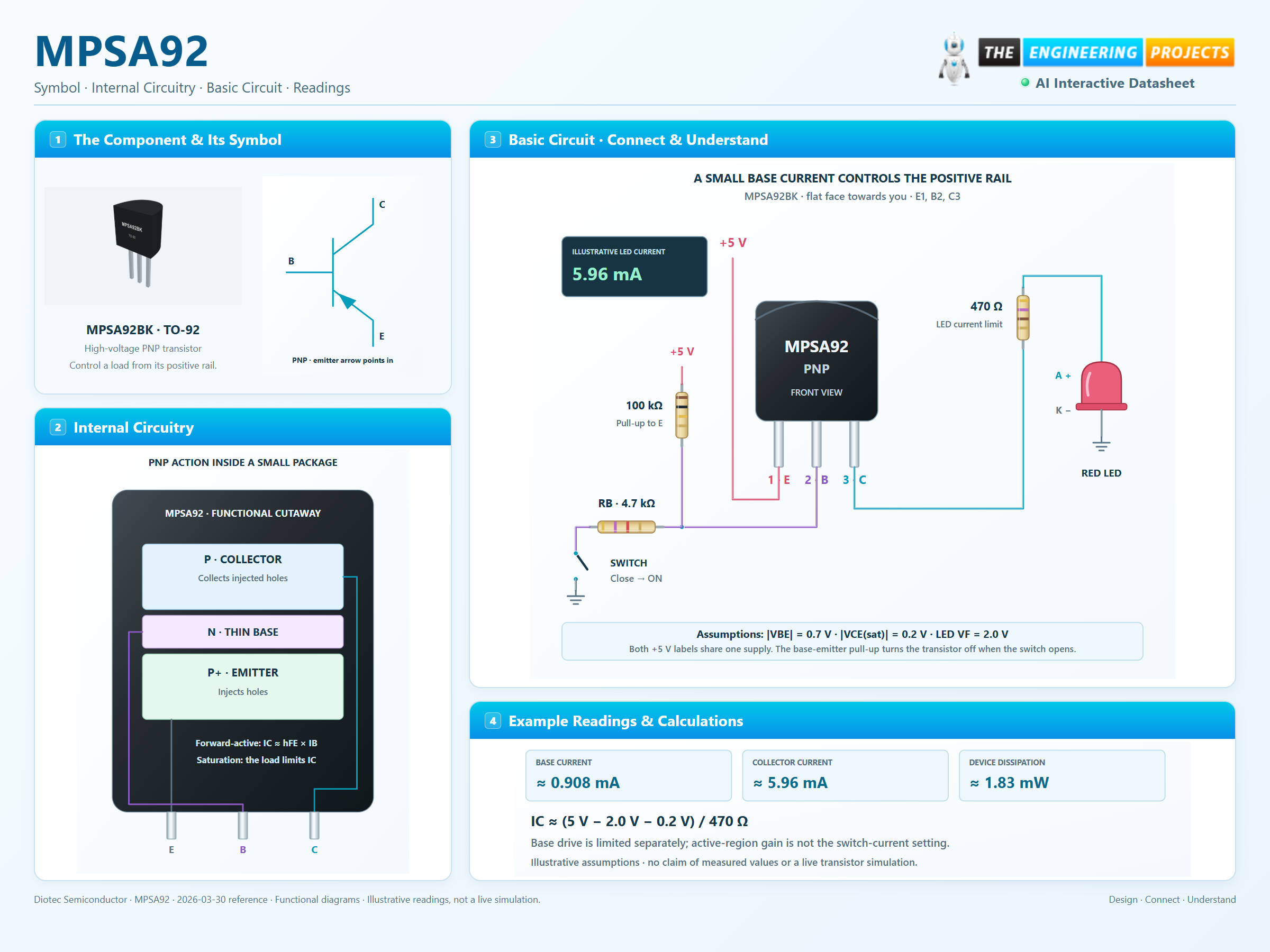
MPSA92 at a glance
Follow the labeled connections and functional stages
How it works
3 stages · Explore one step at a time
Establish the off state
A 100 kΩ resistor connects base to emitter.
Provide base drive
Close the switch to ground through 4.7 kΩ.
Limit the load current
The 470 Ω LED resistor sets current; the transistor does not regulate it.
Step 1 of 3
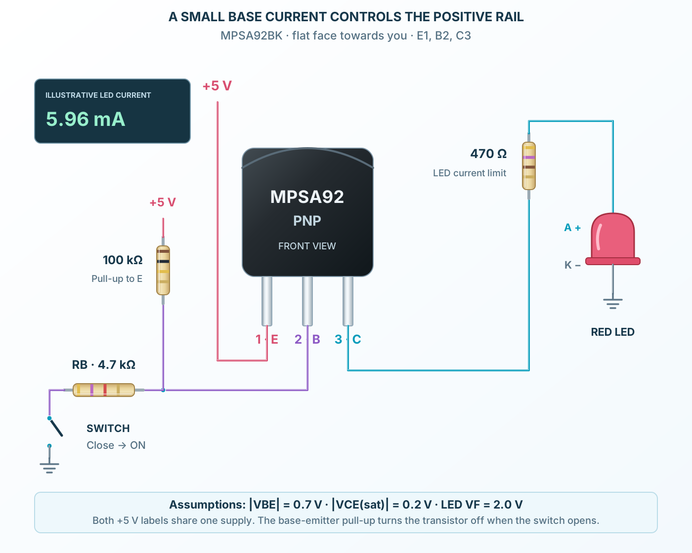
MPSA92 in a circuit
High-side 5 V example with actual TO-92 terminal numbers.
Connect it, step by step
Follow the component values and pin connections
Connect emitter
Emitter 1 to +5 V.
Connect the load
Collector 3 feeds the resistor and LED to ground.
Drive through resistance
A ground switch drives base 2 through 4.7 kΩ; 100 kΩ pulls it to emitter.
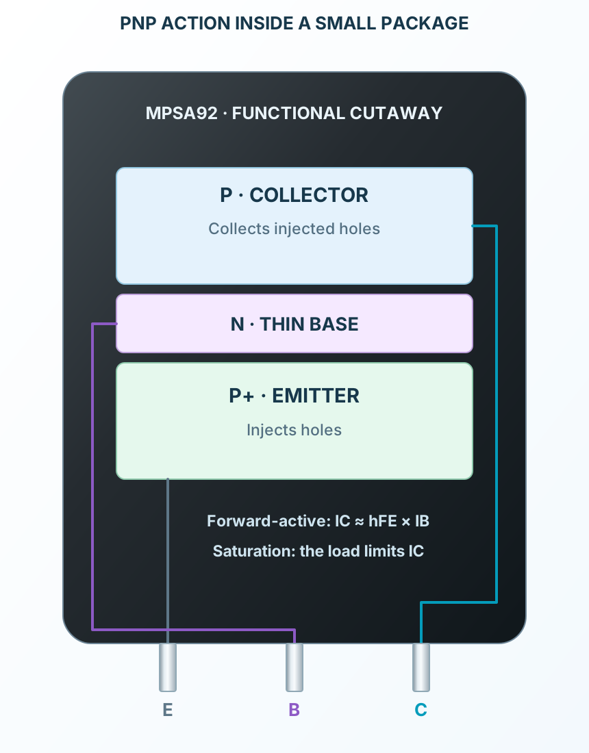
Inside MPSA92
Functional regions kept compact inside the component body.
Explore the circuit
Select a stage to see its role and connections
Emitter injection
Forward bias injects holes into the thin base.
Collector action
Most injected carriers reach the collector in forward-active operation.
Saturation
A switch is driven beyond its linear operating region; the load then limits current.
Selected packageTO-92MPSA92BK
Physical connections3 pinsPackage-specific numbering
Reference collection7 tables40 parameters & pin functions
Pin reference
Signal names, electrical functions and connection guidance
Physical pin numbers3 pins
Scroll within the table to see all columns and rows.
| Pin | Signal | Type | Function & connection |
|---|---|---|---|
| E | Emitter | Emitter terminal of the bipolar transistor.Connection guidanceConnect to +5 V in the high-side example. TO-92 pin 1 becomes SOT-23 pin 2. | |
| B | Base | Base current controls the collector current within the circuit operating region.Connection guidancePull down through 4.7 kΩ to turn on; 100 kΩ returns base to emitter. TO-92 pin 2 becomes SOT-23 pin 1. | |
| C | Collector | Load-current terminal of the transistor.Connection guidanceFeeds the resistor and LED to ground. Collector remains physical pin 3 in both selected packages. |
No pins match these filters. Try another signal name or reset the filters.
Packages and terminal functions
Reviewed Diotec selections
Manufacturer-referenced values4 parameters
Scroll within the table to see all columns and rows.
| Parameter | Value | Conditions / notes |
|---|---|---|
| Through-hole selection | MPSA92BK | Straight-lead TO-92: E1, B2, C3 |
| SMD selection | MMBTA92 | SOT-23: B1, E2, C3 |
| SMD marking | 2D | Manufacturer marking code |
| Polarity | PNP | Magnitudes shown for PNP values |
No specifications match. Try a parameter name or a unit.
Physical pin numbers change between packages; connect by E/B/C function.
TO-92 absolute limits
25°C unless stated
Manufacturer-referenced values6 parameters
Scroll within the table to see all columns and rows.
| Parameter | Value | Conditions / notes |
|---|---|---|
| Collector-emitter / collector-base | 300 / 300 V magnitudes | Base open / emitter open |
| Emitter-base reverse | 5 V magnitude | Collector open |
| DC collector current | 500 mA magnitude | Apply power and junction-temperature limits |
| Power dissipation | 625 mW | Leads held at ambient temperature 2 mm from case |
| Junction temperature | −55 to +150°C | Absolute range |
| Junction-to-ambient | <200 K/W | Manufacturer lead-cooling condition |
No specifications match. Try a parameter name or a unit.
300 V and 500 mA are not a simultaneous operating point.
TO-92 electrical characteristics
25°C · package-specific test points
Manufacturer-referenced values7 parameters
Scroll within the table to see all columns and rows.
| Parameter | Value | Conditions / notes |
|---|---|---|
| Gain at 1 / 10 / 30 mA | ≥25 / ≥40 / ≥25 | |VCE| = 10 V |
| Collector saturation voltage | ≤0.50 V | |IC| = 20 mA; |IB| = 2 mA |
| Base saturation voltage | ≤0.90 V | |IC| = 20 mA; |IB| = 2 mA |
| Collector-base leakage | ≤250 nA | |VCB| = 200 V; emitter open |
| Emitter-base leakage | ≤100 nA | |VEB| = 3 V; see manufacturer terminal-bias condition |
| Transition frequency | 70 MHz typical | |VCE| = 20 V; |IC| = 10 mA; f = 100 MHz |
| Collector-base capacitance | ≤7 pF | |VCB| = 20 V; 1 MHz |
No specifications match. Try a parameter name or a unit.
On-state values use pulsed measurements; typical frequency is not a guaranteed switching rate.
SMD · MMBTA92
Independent manufacturer reference
Manufacturer-referenced values10 parameters
Scroll within the table to see all columns and rows.
| Parameter | Value | Conditions / notes |
|---|---|---|
| VCEO / VCBO / VEBO | 300 / 300 / 6 V magnitudes | Absolute limits with the specified third terminal open |
| DC collector current | 500 mA magnitude | Apply thermal constraints |
| Power dissipation | 250 mW | PCB with 3 mm² copper at each terminal |
| Gain at 10 mA | 80–200 | |VCE| = 10 V |
| Gain at 1 / 30 mA | >25 / >40 | |VCE| = 10 V |
| VCE(sat) / VBE(sat) | <0.50 / <0.90 V | |IC| = 20 mA; |IB| = 2 mA |
| Transition frequency | >50 MHz | |VCE| = 20 V; |IC| = 10 mA; f = 100 MHz |
| Collector-base capacitance | <3 pF | |VCB| = 20 V; 1 MHz |
| Junction / storage | −55 to +150°C | Absolute ranges |
| Body / full lead span | 2.9 × 1.3 / 2.4 mm nominal | Paired-contact pitch 1.9 mm |
No specifications match. Try a parameter name or a unit.
SMD values belong to the exact listed part; do not substitute the axial thermal rating.
TO-92 mechanical reference
Manufacturer straight-lead drawing
Manufacturer-referenced values6 parameters
Scroll within the table to see all columns and rows.
| Parameter | Value | Conditions / notes |
|---|---|---|
| Body width / height | 4.6 ±0.1 / 4.6 ±0.1 mm | Black flat-front molded body |
| Body depth | 3.6 ±0.1 mm | Flat face 1.1 ±0.2 mm from lead plane |
| Lead pitch | 1.27 ±0.1 mm | Straight-lead option |
| Lead width / thickness | 0.4 +0.15/−0.05 / 0.34 ±0.05 mm | Silver plated stamped contacts |
| Supplied lead length | ≥12.5 mm | Preview shows trimmed leads for readability |
| Authored pad / hole | 1.10 × 1.55 / 0.80 mm | Engineering footprint; review fabrication tolerance |
No specifications match. Try a parameter name or a unit.
The 2.54 mm formed tape option is a different mounting geometry.
5 V LED example
Teaching assumptions, not measured values
Manufacturer-referenced values7 parameters
Scroll within the table to see all columns and rows.
| Parameter | Value | Conditions / notes |
|---|---|---|
| Load / base / bias resistors | 470 Ω / 4.7 kΩ / 100 kΩ | Use separate current limits |
| Assumed drops | LED 2.0 V; |VBE| 0.7 V; |VCE(sat)| 0.2 V | Actual drops vary |
| Collector current | 5.96 mA | (5 − 2 − 0.2) / 470 |
| Net base current | 0.908 mA | (5 − 0.7) / 4700 − 0.7 / 100000 |
| Forced current ratio | Approximately 6.56 | Collector / base current |
| Transistor dissipation | Approximately 1.83 mW | Collector-emitter plus base-emitter terms |
| Inductive loads | Require a revised circuit | Add suitable flyback protection; not pictured here |
No specifications match. Try a parameter name or a unit.
The example is a low-current LED switch; it does not demonstrate the maximum-current rating.
No matching rowsTry a pin name, parameter, unit or test condition, or reset the filters.
Signal amplification
Set the bias point, load and dissipation for the required signal swing.
Manufacturer application guideLevel interfaces
Use the high collector-voltage capability with deliberate current limiting and appropriate physical spacing.
Manufacturer application guideLow-voltage demonstration
The 5 V LED circuit illustrates control polarity and current limiting without using the maximum voltage rating.
Manufacturer application guideTake it into ProTech
Find MPSA92 in the Components Library to place its schematic symbol and connect its pins.
Reference page · circuit simulation model not yet availableOpen ProTech