OP07Precision bipolar operational amplifier
Small input errors matter. Build a clearer precision signal path.
OP07 is a precision operational-amplifier family using a low-noise bipolar input stage and internal compensation. Negative feedback produces a controlled analog gain while low offset and drift help preserve small DC signals. It is a precision amplifier rather than a rail-to-rail or high-speed device. This page selects TI OP07CP in PDIP-8 and OP07CDR in SOIC-8, both commercial C-grade parts. Offset trim uses pins 1 and 8; pin 5 is unconnected. Package views and footprints preserve this mapping, which differs from the familiar LM741 trim arrangement. The example uses ±15 V rails, 90 kΩ feedback and 10 kΩ to the 0 V midpoint. A 0.20 V input gives an ideal 2.00 V output. The reference tables distinguish typical values from guaranteed limits; precision also depends on resistor accuracy, leakage, thermal gradients and the measurement setup.
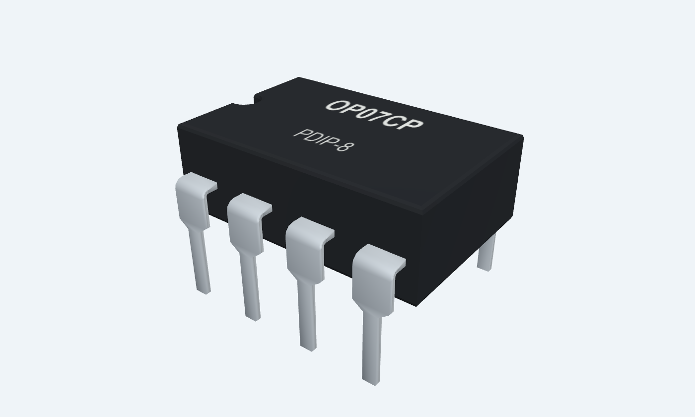
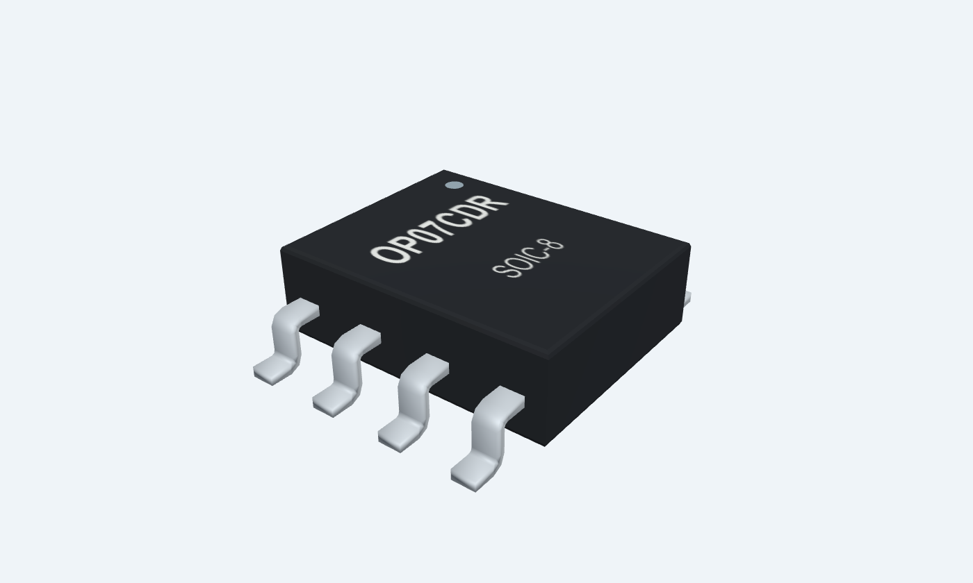

8Physical pins
OP07CPPDIP-8
Manufacturer-referencedTexas Instruments
Pin diagram
Select a pin to explore its connection
Highlight
OP07CPPDIP-8Top view
OP07CDRSOIC-8Top view
Click a lead or use the arrow keys. Top view
PIN 1 · Optional offset trim
Optional offset adjustmentNULL1
Function
First terminal of the optional input-offset trim network.
How to connect
Leave open in the illustrated circuit.
Electrical note
Use TI’s trim network only when needed; its other end is pin 8.
PIN 2 · Signal inputs
Inverting inputIN−
Function
Negative-feedback summing node.
How to connect
Connect the 90 kΩ/10 kΩ resistor junction.
PIN 3 · Signal inputs
Non-inverting inputIN+
Function
Positive signal input.
How to connect
Apply 0.20 V relative to the 0 V supply midpoint.
PIN 4 · Supply
Negative supplyV−
Function
Negative power rail.
How to connect
Connect −15 V; bypass locally to 0 V with 100 nF.
Electrical note
Not signal ground in this circuit.
PIN 5 · Not connected
No connectionNC
Function
No electrical connection is specified for this pin.
How to connect
Leave unconnected.
PIN 6 · Analog output
Analog outputOUT
Function
Amplifier output and feedback source.
How to connect
Connect 90 kΩ to IN− 2 and a high-impedance output meter.
PIN 7 · Supply
Positive supplyV+
Function
Positive power rail.
How to connect
Connect +15 V; bypass locally to 0 V with 100 nF.
PIN 8 · Optional offset trim
Optional offset adjustmentNULL2
Function
Second terminal of the optional input-offset trim network.
How to connect
Leave open in the illustrated circuit.
Electrical note
Paired with pin 1; this is not the LM741 null-pin arrangement.
Key specifications
Input offset is only one error term. Include bias-current drops, resistor ratios, thermal gradients and loading before treating a result as accurate.
C-grade typical offset±60 µV ·25°C; not a maximum
Recommended split rails±3–±18 V
Ambient operating range0–70 °C
Typical voltage noise9.8 nV/√Hz ·1 kHz
Package details
OP07CP · PDIP-8
| Property | Details |
|---|---|
| Manufacturer | Texas Instruments |
| Part number | OP07CP |
| Package | PDIP-8 |
| Connections | 8 pins |
| Mounting | Through-hole |
| Lead pitch | 2.54 mm |
| Package code | dip |
| Thermal reference | θJA85°C/W on TI reference board |
Supply and operating conditions
TI OP07C reference
Manufacturer specifications 7 parameters
Scroll sideways to see all columns.
| Parameter | Value | Conditions / notes |
|---|---|---|
| Recommended split supply | ±3 to±18 V | 6–36 V total span |
| Example rails | ±15 V | 0 V midpoint is signal ground |
| Ambient range | 0–70°C | Selected commercial C grade |
| Common-mode recommended at±15 V | −13 to+13 V | Do not infer rail-to-rail operation |
| Absolute supply maximum | ±22 V | Stress limit, not an operating target |
| Input absolute limit note | Magnitude no greater than supply or15 V, whichever is less | Manufacturer footnote applies |
| Local bypass | 100 nF per rail to 0 V | Short return paths near pins 7 and 4 |
No specifications match. Try a parameter name or a unit.
Do not substitute the absolute stress values for recommended operation.
C-grade input accuracy
±15 V,25°C unless stated; column labels retained
Manufacturer specifications 7 parameters
Scroll sideways to see all columns.
| Parameter | Value | Conditions / notes |
|---|---|---|
| Input offset voltage | ±60 µV typical | ±85 µV typical across0–70°C |
| Offset drift | ±0.5 µV/°C typical | C grade; not a guaranteed maximum |
| Long-term offset drift | ±0.4 µV/month typical estimate | Average trend after first30 days; not individually guaranteed |
| Input bias current | ±1.8 nA typical | ±2.2 nA typical across0–70°C |
| Input offset current | ±0.8 nA typical | ±1.6 nA typical across0–70°C |
| Bias-current drift | ±18 pA/°C typical | C-grade table |
| Offset adjustment range | ±4 mV typical | Rs20 kΩ; optional manufacturer trim network |
No specifications match. Try a parameter name or a unit.
TI revision H places these C-grade values in the typical column. They are not maximum-error guarantees.
Noise and rejection
Use the bandwidth and source conditions
Manufacturer specifications 8 parameters
Scroll sideways to see all columns.
| Parameter | Value | Conditions / notes |
|---|---|---|
| Voltage noise,0.1–10 Hz | 0.38 µV peak-to-peak typical | Not RMS |
| Voltage noise density at10 Hz | 10.5 nV/√Hz typical | Input-referred |
| Voltage noise density at1 kHz | 9.8 nV/√Hz typical | Input-referred |
| Current noise density at1 kHz | 0.13 pA/√Hz typical | Source resistance converts it to voltage noise |
| C-grade CMRR at25°C | 100 dB minimum;120 dB typical | VCM±13 V |
| C-grade CMRR over0–70°C | 97 dB minimum;120 dB typical | VCM±13 V |
| Supply sensitivity at25°C | 7 µV/V typical;32 µV/V maximum | VS±3 to±18 V |
| Supply sensitivity over0–70°C | 10 µV/V typical;51 µV/V maximum | Lower is better; table usesµV/V |
No specifications match. Try a parameter name or a unit.
Noise densities must be integrated over the circuit bandwidth.
Speed, loading and power
Manufacturer test conditions
Manufacturer specifications 7 parameters
Scroll sideways to see all columns.
| Parameter | Value | Conditions / notes |
|---|---|---|
| Unity-gain bandwidth | 0.4 MHz minimum;0.6 MHz typical | Standard table conditions |
| Slew rate | 0.3 V/µs typical | VS5 V;RL2 kΩ per source table |
| Output swing at25°C,RL2 kΩ | ±11.5 V minimum;±12.8 V typical | VS±15 V |
| Output swing over0–70°C,RL2 kΩ | ±11 V minimum;±12.6 V typical | VS±15 V |
| Output swing atRL10 kΩ | ±12 V minimum;±13 V typical | VS±15 V |
| No-load device power at±15 V | 80 mW typical;150 mW maximum | Not output power |
| No-load device power at±3 V | 4 mW typical;8 mW maximum | Lower-supply condition |
No specifications match. Try a parameter name or a unit.
Check headroom and settling; this is not a high-speed amplifier.
Gain-of-ten precision example
Calculated DC illustration
Manufacturer specifications 7 parameters
Scroll sideways to see all columns.
| Parameter | Value | Conditions / notes |
|---|---|---|
| VIN | 0.20 V | Non-inverting pin 3 |
| Feedback resistor | 90 kΩ | OUT 6 to IN− 2 |
| Ground resistor | 10 kΩ | IN− 2 to 0 V midpoint |
| Ideal gain | 10 V/V | 1+90/10 |
| Ideal output | 2.00 V | 0.20×10 |
| Typical offset contribution | About0.60 mV at output | 60 µV×noise gain 10; not total error |
| Unused trim / NC | 1 and 8 open; 5 unconnected | Optional offset adjustment omitted |
No specifications match. Try a parameter name or a unit.
Select resistor ratio tolerance for the required accuracy; the illustration is not calibrated hardware.
Package pins and board practice
OP07CP ·PDIP-8
Manufacturer specifications 7 parameters
Scroll sideways to see all columns.
| Parameter | Value | Conditions / notes |
|---|---|---|
| Lead pitch | 2.54 mm | Through-hole |
| Input pair | 2 IN−;3 IN+ | Keep leakage and contamination low |
| Supply | 4 V−;7 V+ | Both locally bypassed |
| Output | 6 | Return feedback close to the input network |
| Optional trim | 1 NULL1;8 NULL2 | Follow the exact manufacturer circuit |
| No connection | 5 | Leave open |
| Thermal layout | Avoid uneven heating near input nodes | Thermoelectric voltages can matter at µV levels |
No specifications match. Try a parameter name or a unit.
Top view, counterclockwise numbering; pin 1 at the marker.
Connections by function
Select a pin for its function, connection guidance and electrical notes.
Optional offset trim2 pins
Signal inputs2 pins
Supply2 pins
Not connected1 pin
Analog output1 pin
Optional offset trim2 pins
Signal inputs2 pins
Supply2 pins
Not connected1 pin
Analog output1 pin
OP07 at a glance
Follow the labeled connections and functional stages
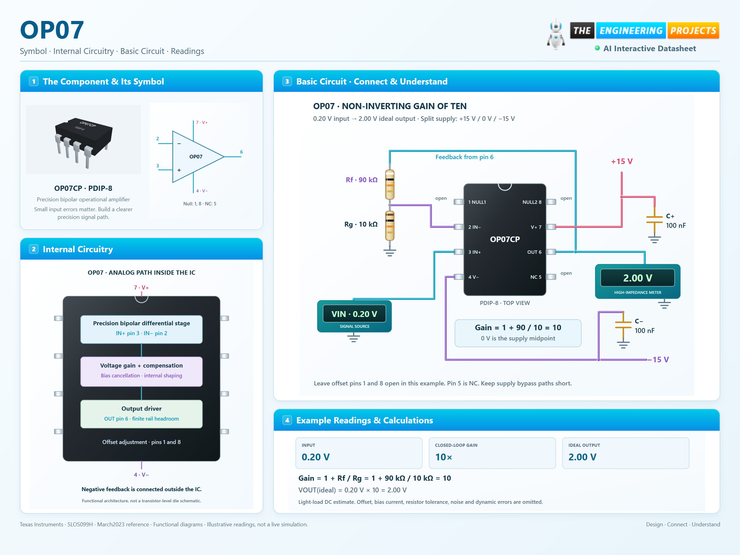
How it works
3 stages · Explore one step at a time
Compare the inputs
The bipolar input stage responds to the difference between pins 3 and 2.
Close the feedback loop
90 kΩ from OUT 6 to IN− 2 and 10 kΩ from IN− 2 to 0 V give a noise gain of ten.
Budget real errors
Check offset, input currents, resistor tolerance, temperature and settling before reading a small signal.
Step 1 of 3
OP07 in a circuit
A physical eight-pin IC, feedback resistors and local bypass.
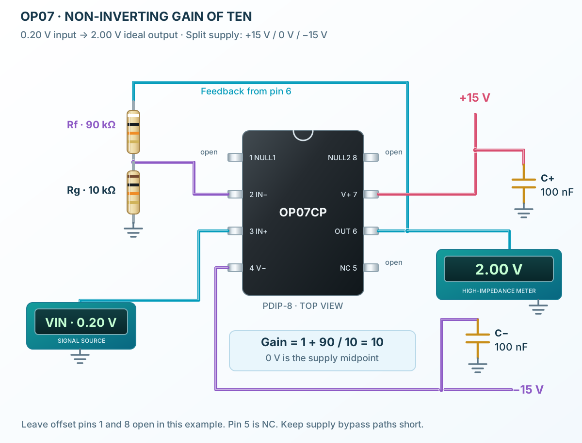
Connect it, step by step
Follow the component values and pin connections
Supply
Apply ±15 V to7 and 4; bypass both rails to 0 V.
Feedback
Use 90 kΩ/10 kΩ for gain ten.
Measure
Read near 2.00 V with a high-impedance meter; include device and resistor errors.
Inside OP07
Precision bipolar inputs and compensated gain within the IC.
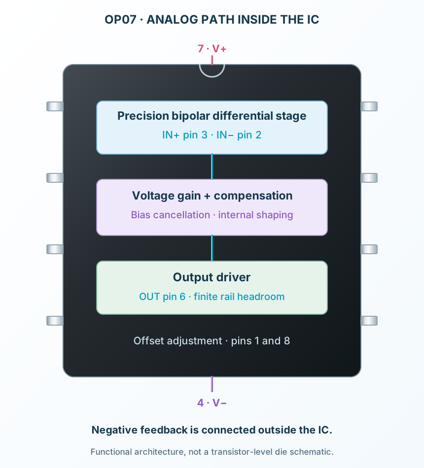
Explore the circuit
Select a stage to see its role and connections
Sense
The input stage senses a small differential voltage with bias-current cancellation.
Amplify
Internally compensated gain supports ordinary closed-loop operation.
Drive
The output stage drives the feedback network and compatible load.
Selected packagePDIP-8OP07CP
Physical connections8 pinsPackage-specific numbering
Reference collection7 tables43 parameters & pin functions
Pin reference
Signal names, electrical functions and connection guidance
Physical pin numbers8 pins
Scroll within the table to see all columns and rows.
| Pin | Signal | Type | Function & connection |
|---|---|---|---|
| NULL1 | Optional offset adjustment | First terminal of the optional input-offset trim network.Connection guidanceLeave open in the illustrated circuit. Use TI’s trim network only when needed; its other end is pin 8. | |
| IN− | Inverting input | Negative-feedback summing node.Connection guidanceConnect the 90 kΩ/10 kΩ resistor junction. | |
| IN+ | Non-inverting input | Positive signal input.Connection guidanceApply 0.20 V relative to the 0 V supply midpoint. | |
| V− | Negative supply | Negative power rail.Connection guidanceConnect −15 V; bypass locally to 0 V with 100 nF. Not signal ground in this circuit. | |
| NC | No connection | No electrical connection is specified for this pin.Connection guidanceLeave unconnected. | |
| OUT | Analog output | Amplifier output and feedback source.Connection guidanceConnect 90 kΩ to IN− 2 and a high-impedance output meter. | |
| V+ | Positive supply | Positive power rail.Connection guidanceConnect +15 V; bypass locally to 0 V with 100 nF. | |
| NULL2 | Optional offset adjustment | Second terminal of the optional input-offset trim network.Connection guidanceLeave open in the illustrated circuit. Paired with pin 1; this is not the LM741 null-pin arrangement. |
No pins match these filters. Try another signal name or reset the filters.
Supply and operating conditions
TI OP07C reference
Manufacturer-referenced values7 parameters
Scroll within the table to see all columns and rows.
| Parameter | Value | Conditions / notes |
|---|---|---|
| Recommended split supply | ±3 to±18 V | 6–36 V total span |
| Example rails | ±15 V | 0 V midpoint is signal ground |
| Ambient range | 0–70°C | Selected commercial C grade |
| Common-mode recommended at±15 V | −13 to+13 V | Do not infer rail-to-rail operation |
| Absolute supply maximum | ±22 V | Stress limit, not an operating target |
| Input absolute limit note | Magnitude no greater than supply or15 V, whichever is less | Manufacturer footnote applies |
| Local bypass | 100 nF per rail to 0 V | Short return paths near pins 7 and 4 |
No specifications match. Try a parameter name or a unit.
Do not substitute the absolute stress values for recommended operation.
C-grade input accuracy
±15 V,25°C unless stated; column labels retained
Manufacturer-referenced values7 parameters
Scroll within the table to see all columns and rows.
| Parameter | Value | Conditions / notes |
|---|---|---|
| Input offset voltage | ±60 µV typical | ±85 µV typical across0–70°C |
| Offset drift | ±0.5 µV/°C typical | C grade; not a guaranteed maximum |
| Long-term offset drift | ±0.4 µV/month typical estimate | Average trend after first30 days; not individually guaranteed |
| Input bias current | ±1.8 nA typical | ±2.2 nA typical across0–70°C |
| Input offset current | ±0.8 nA typical | ±1.6 nA typical across0–70°C |
| Bias-current drift | ±18 pA/°C typical | C-grade table |
| Offset adjustment range | ±4 mV typical | Rs20 kΩ; optional manufacturer trim network |
No specifications match. Try a parameter name or a unit.
TI revision H places these C-grade values in the typical column. They are not maximum-error guarantees.
Noise and rejection
Use the bandwidth and source conditions
Manufacturer-referenced values8 parameters
Scroll within the table to see all columns and rows.
| Parameter | Value | Conditions / notes |
|---|---|---|
| Voltage noise,0.1–10 Hz | 0.38 µV peak-to-peak typical | Not RMS |
| Voltage noise density at10 Hz | 10.5 nV/√Hz typical | Input-referred |
| Voltage noise density at1 kHz | 9.8 nV/√Hz typical | Input-referred |
| Current noise density at1 kHz | 0.13 pA/√Hz typical | Source resistance converts it to voltage noise |
| C-grade CMRR at25°C | 100 dB minimum;120 dB typical | VCM±13 V |
| C-grade CMRR over0–70°C | 97 dB minimum;120 dB typical | VCM±13 V |
| Supply sensitivity at25°C | 7 µV/V typical;32 µV/V maximum | VS±3 to±18 V |
| Supply sensitivity over0–70°C | 10 µV/V typical;51 µV/V maximum | Lower is better; table usesµV/V |
No specifications match. Try a parameter name or a unit.
Noise densities must be integrated over the circuit bandwidth.
Speed, loading and power
Manufacturer test conditions
Manufacturer-referenced values7 parameters
Scroll within the table to see all columns and rows.
| Parameter | Value | Conditions / notes |
|---|---|---|
| Unity-gain bandwidth | 0.4 MHz minimum;0.6 MHz typical | Standard table conditions |
| Slew rate | 0.3 V/µs typical | VS5 V;RL2 kΩ per source table |
| Output swing at25°C,RL2 kΩ | ±11.5 V minimum;±12.8 V typical | VS±15 V |
| Output swing over0–70°C,RL2 kΩ | ±11 V minimum;±12.6 V typical | VS±15 V |
| Output swing atRL10 kΩ | ±12 V minimum;±13 V typical | VS±15 V |
| No-load device power at±15 V | 80 mW typical;150 mW maximum | Not output power |
| No-load device power at±3 V | 4 mW typical;8 mW maximum | Lower-supply condition |
No specifications match. Try a parameter name or a unit.
Check headroom and settling; this is not a high-speed amplifier.
Gain-of-ten precision example
Calculated DC illustration
Manufacturer-referenced values7 parameters
Scroll within the table to see all columns and rows.
| Parameter | Value | Conditions / notes |
|---|---|---|
| VIN | 0.20 V | Non-inverting pin 3 |
| Feedback resistor | 90 kΩ | OUT 6 to IN− 2 |
| Ground resistor | 10 kΩ | IN− 2 to 0 V midpoint |
| Ideal gain | 10 V/V | 1+90/10 |
| Ideal output | 2.00 V | 0.20×10 |
| Typical offset contribution | About0.60 mV at output | 60 µV×noise gain 10; not total error |
| Unused trim / NC | 1 and 8 open; 5 unconnected | Optional offset adjustment omitted |
No specifications match. Try a parameter name or a unit.
Select resistor ratio tolerance for the required accuracy; the illustration is not calibrated hardware.
Package pins and board practice
OP07CP ·PDIP-8
Manufacturer-referenced values7 parameters
Scroll within the table to see all columns and rows.
| Parameter | Value | Conditions / notes |
|---|---|---|
| Lead pitch | 2.54 mm | Through-hole |
| Input pair | 2 IN−;3 IN+ | Keep leakage and contamination low |
| Supply | 4 V−;7 V+ | Both locally bypassed |
| Output | 6 | Return feedback close to the input network |
| Optional trim | 1 NULL1;8 NULL2 | Follow the exact manufacturer circuit |
| No connection | 5 | Leave open |
| Thermal layout | Avoid uneven heating near input nodes | Thermoelectric voltages can matter at µV levels |
No specifications match. Try a parameter name or a unit.
Top view, counterclockwise numbering; pin 1 at the marker.
No matching rowsTry a pin name, parameter, unit or test condition, or reset the filters.
DC instrumentation
Condition small, slow signals with a complete offset and resistor error budget.
Manufacturer application guidePrecision buffers
Buffer compatible voltage references while accounting for loading and input current.
Manufacturer application guideSensor interfaces
Amplify low-frequency sensor outputs while controlling leakage and thermal gradients.
Manufacturer application guideTake it into ProTech
Find OP07 in the Components Library to place its schematic symbol and connect its pins.
Reference page · circuit simulation model not yet availableOpen ProTech