Real View
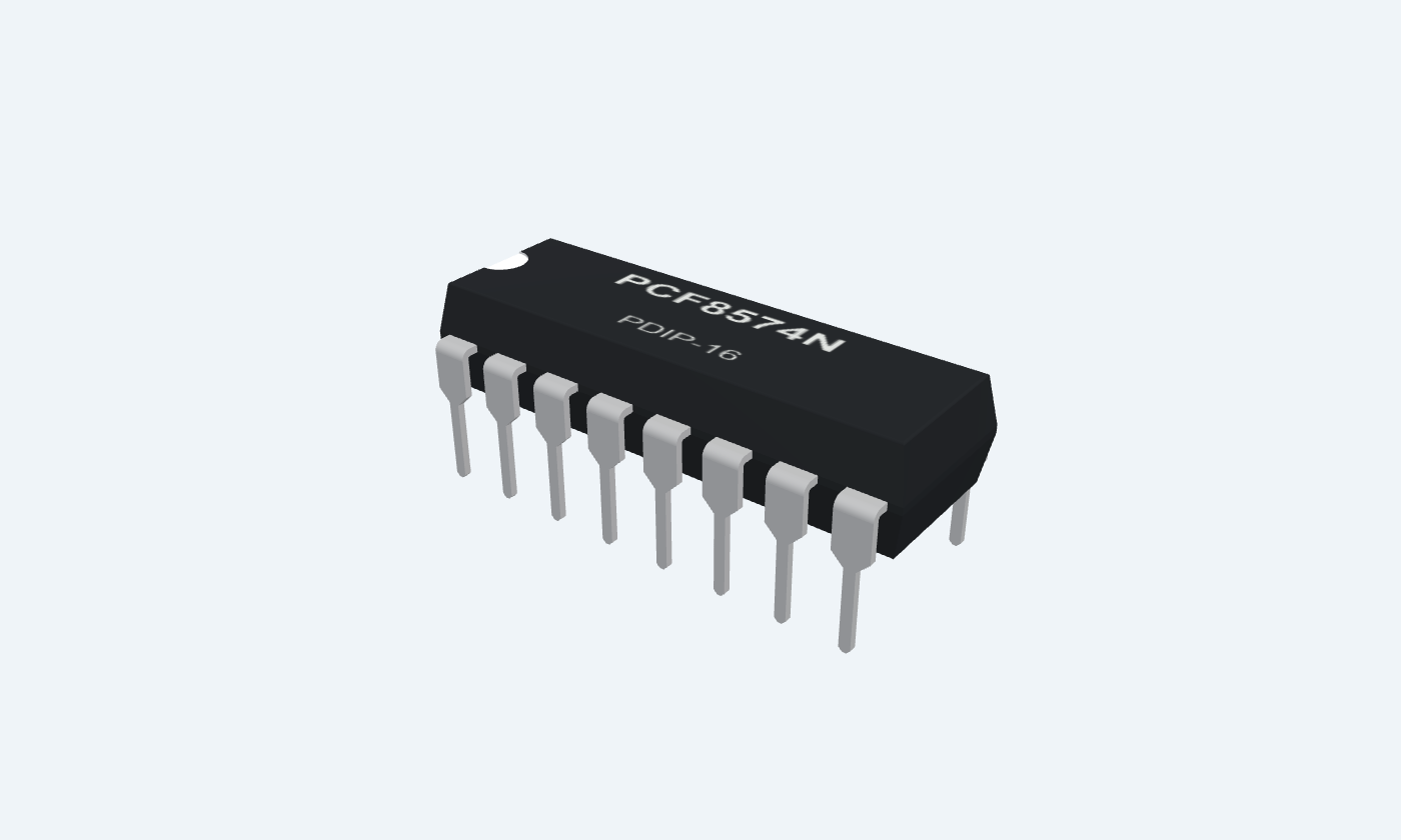
Add eight simple I/O lines through a two-wire bus.
PCF8574 adds eight quasi-bidirectional I/O lines to a standard-mode I²C bus. A controller reads or writes one port byte directly after the device address; there is no direction register or register-address byte. Three hardware address pins allow eight PCF8574 devices on one bus. Writing a port bit LOW turns on its sink driver. Writing it HIGH releases the pin with a weak current-source pull-up, allowing an external switch or device to pull it LOW for input use. All port bits start HIGH after power-on, and software must keep input bits HIGH in every subsequent output write. The example uses one port bit to sink a current-limited LED and another to read a grounded pushbutton. An open-drain interrupt reports input changes. The expander, controller and pull-ups share a 5 V logic domain; using another controller voltage requires a compatible supply choice or suitable level translation.
Select a pin to explore its connection
Click a lead or use the arrow keys. Top view
Sets bit 0 of the 7-bit I²C address. Tie directly to VCC or GND.
Ground all three address inputs for address 0x20.
Keep stable throughout a bus transaction.
Sets bit 1 of the 7-bit I²C address. Tie directly to VCC or GND.
Ground all three address inputs for address 0x20.
Keep stable throughout a bus transaction.
Sets bit 2 of the 7-bit I²C address. Tie directly to VCC or GND.
Ground all three address inputs for address 0x20.
Keep stable throughout a bus transaction.
Port bit 0. Writing 0 actively sinks; writing 1 releases the pin with its weak current-source pull-up so it can be read as an input.
Connect LED cathode; LED anode reaches +5 V through 1 kΩ.
Not a conventional push-pull HIGH output; preserve input bits as 1 in every output write.
Port bit 1. Writing 0 actively sinks; writing 1 releases the pin with its weak current-source pull-up so it can be read as an input.
Connect a pushbutton to GND and leave its output-latch bit HIGH.
Not a conventional push-pull HIGH output; preserve input bits as 1 in every output write.
Port bit 2. Writing 0 actively sinks; writing 1 releases the pin with its weak current-source pull-up so it can be read as an input.
Leave unused pins open with their latch bits HIGH.
Not a conventional push-pull HIGH output; preserve input bits as 1 in every output write.
Port bit 3. Writing 0 actively sinks; writing 1 releases the pin with its weak current-source pull-up so it can be read as an input.
Leave unused pins open with their latch bits HIGH.
Not a conventional push-pull HIGH output; preserve input bits as 1 in every output write.
Supply and signal reference.
Connect to controller ground.
Port bit 4. Writing 0 actively sinks; writing 1 releases the pin with its weak current-source pull-up so it can be read as an input.
Leave unused pins open with their latch bits HIGH.
Not a conventional push-pull HIGH output; preserve input bits as 1 in every output write.
Port bit 5. Writing 0 actively sinks; writing 1 releases the pin with its weak current-source pull-up so it can be read as an input.
Leave unused pins open with their latch bits HIGH.
Not a conventional push-pull HIGH output; preserve input bits as 1 in every output write.
Port bit 6. Writing 0 actively sinks; writing 1 releases the pin with its weak current-source pull-up so it can be read as an input.
Leave unused pins open with their latch bits HIGH.
Not a conventional push-pull HIGH output; preserve input bits as 1 in every output write.
Port bit 7. Writing 0 actively sinks; writing 1 releases the pin with its weak current-source pull-up so it can be read as an input.
Leave unused pins open with their latch bits HIGH.
Not a conventional push-pull HIGH output; preserve input bits as 1 in every output write.
Asserts LOW after a change on an input port. Reading/writing the port or return to its original state resets the interrupt as described in the data sheet.
Pull up with 10 kΩ to +5 V and connect to a 5 V-compatible interrupt input.
Edges during the acknowledge/reset interval may be lost; read the port and debounce buttons.
Standard-mode serial clock, up to 100 kHz.
Connect controller SCL with a suitable pull-up to VCC.
Bidirectional open-drain serial data.
Connect controller SDA with a suitable pull-up to VCC.
Operates from 2.5 V to 6 V.
Use +5 V for this example and 100 nF directly to GND pin 8.
At 5 V, the specified input HIGH threshold is 3.5 V; do not assume a 3.3 V HIGH is sufficient.
Each port bit combines an output latch, a sink driver and a weak HIGH current source. Writing 1 prepares an input; writing 0 actively pulls the terminal LOW.
PCF8574N · PDIP-16
| Property | Details |
|---|---|
| Manufacturer | Texas Instruments |
| Part number | PCF8574N |
| Package | PDIP-16 |
| Connections | 16 pins |
| Mounting | Through-hole |
| Lead pitch | 2.54 mm |
| Package code | dip |
| Thermal reference | Board and package dependent; see manufacturer data |
Quasi-bidirectional operation
Scroll sideways to see all columns.
| Parameter | Value | Conditions / notes |
|---|---|---|
| Latch bit 0 | Active LOW sink | Suitable for sinking a current-limited LED |
| Latch bit 1 | Weak current-source HIGH | Can be pulled LOW externally and used as input |
| Power-on state | All latch bits HIGH | Pins behave as inputs with weak HIGH sources |
| Direction registers | None | Direction follows the output-latch state |
| Read value | Actual terminal levels | May differ from the software output shadow |
| Output update | Whole 8-bit byte | Keep all input bits HIGH in every write |
No specifications match. Try a parameter name or a unit.
HIGH is not a sustained strong push-pull output. The temporary strong pull-up assists a rising edge only.
7-bit addresses; do not include the R/W bit
Scroll sideways to see all columns.
| Parameter | Value | Conditions / notes |
|---|---|---|
| A2 A1 A0 = 000 | 0x20 | Write byte 0x40 · read byte 0x41 |
| A2 A1 A0 = 001 | 0x21 | Write byte 0x42 · read byte 0x43 |
| A2 A1 A0 = 010 | 0x22 | Write byte 0x44 · read byte 0x45 |
| A2 A1 A0 = 011 | 0x23 | Write byte 0x46 · read byte 0x47 |
| A2 A1 A0 = 100 | 0x24 | Write byte 0x48 · read byte 0x49 |
| A2 A1 A0 = 101 | 0x25 | Write byte 0x4a · read byte 0x4b |
| A2 A1 A0 = 110 | 0x26 | Write byte 0x4c · read byte 0x4d |
| A2 A1 A0 = 111 | 0x27 | Write byte 0x4e · read byte 0x4f |
No specifications match. Try a parameter name or a unit.
PCF8574A has a different address block. This page uses PCF8574.
Address pins grounded · 7-bit address 0x20
Scroll sideways to see all columns.
| Parameter | Value | Conditions / notes |
|---|---|---|
| LED off; inputs released | Write 0xFF | All port latches HIGH |
| LED on at P0 | Write 0xFE | P0 LOW; P1–P7 remain HIGH |
| Read the button | Read one byte; inspect bit 1 | P1 LOW when the grounded button is pressed |
| Typical pressed read with LED on | 0xFC | Assumes other released inputs read HIGH |
| Transfer structure | START → address → data → STOP | No register-address byte |
| INT servicing | Read port, process changes, debounce | Read/write or return to original state can reset INT |
No specifications match. Try a parameter name or a unit.
The example values describe the stated wiring. Do not use a read byte as an unfiltered output-latch shadow.
Recommended operation unless marked otherwise
Scroll sideways to see all columns.
| Parameter | Value | Conditions / notes |
|---|---|---|
| VCC | 2.5–6 V | Example uses 5 V |
| Input HIGH / LOW | ≥ 0.7 VCC / ≤ 0.3 VCC | Supply-dependent logic thresholds |
| P-port weak HIGH source | 30–310 µA magnitude | At VO = GND, VCC 2.5–6 V |
| P-port sink | 10 mA minimum; 25 mA typical | At VCC 5 V, VO 1 V |
| Recommended LOW current | 25 mA maximum per port | Observe total device and thermal limits |
| SDA sink | 3 mA minimum | At VOL 0.4 V |
| INT sink | 1.6 mA minimum | At VOL 0.4 V |
| Standby supply current | 2.5 µA typical; 10 µA maximum | VCC 6 V; inputs at rails; unloaded |
| Operating supply current | 40 µA typical; 100 µA maximum | VCC 6 V; 100 kHz clock; unloaded |
No specifications match. Try a parameter name or a unit.
Do not interpret the absolute 50 mA port rating as a design target.
Standard-mode I²C
Scroll sideways to see all columns.
| Parameter | Value | Conditions / notes |
|---|---|---|
| SCL frequency | 100 kHz maximum | Not a 400 kHz fast-mode expander |
| SCL LOW / HIGH | 4.7 µs / 4.0 µs minimum | Timing requirements |
| SDA setup | 250 ns minimum | Before SCL rises |
| Bus rise time | 1 µs maximum | Choose pull-ups for capacitance and sink current |
| Maximum bus capacitance | 400 pF | Requires a compatible pull-up value |
| Example pull-ups | 4.7 kΩ on SDA and SCL | About 0.40 µs rise at an assumed 100 pF |
| Port / interrupt delay | 4 µs maximum | Specified switching-test conditions |
No specifications match. Try a parameter name or a unit.
The example 4.7 kΩ is a starting value for a short bus, not a guarantee at the full 400 pF limit.
5 V controller and expander
Scroll sideways to see all columns.
| Parameter | Value | Conditions / notes |
|---|---|---|
| Supply | VCC16 +5 V; GND8 common | 100 nF local bypass |
| Address | A0 pin1, A1 pin2, A2 pin3 to GND | Selects 0x20 |
| SDA15 / SCL14 | Controller I²C bus | Each has a 4.7 kΩ pull-up to +5 V |
| INT13 | Controller interrupt input | 10 kΩ pull-up to +5 V |
| P0 pin4 | LED cathode | Anode via 1 kΩ to +5 V; LOW turns it on |
| P1 pin5 | Pushbutton to GND | Write latch bit 1 before reading; debounce |
| P2–P7 | Unused in this example | Leave open and maintain latch bits HIGH |
No specifications match. Try a parameter name or a unit.
At assumed VF 2 V and VOL 0.2 V, LED current is (5 − 2 − 0.2)/1k = 2.8 mA. Actual values depend on the LED and port.
PCF8574N · PDIP-16
Scroll sideways to see all columns.
| Parameter | Value | Conditions / notes |
|---|---|---|
| N package | PDIP-16; 2.54 mm pitch | Through-hole view shown |
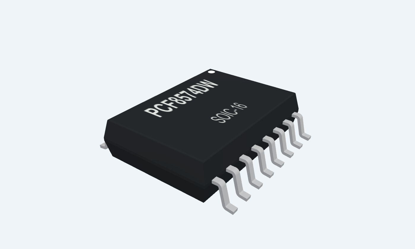
| DW package | Wide SOIC-16; 1.27 mm pitch | 7.5 mm nominal body width |
| PW / DGV alternatives | 20 physical leads | Different mapping with unused pins; not shown |
| VCC absolute maximum | 6.5 V | Normal recommended maximum is 6 V |
| Continuous supply/ground current | ±100 mA absolute maximum | Stress rating; sum all loads |
| Storage temperature | −65 to +150°C | Unpowered |
No specifications match. Try a parameter name or a unit.
The two selected 16-pin packages share logical pin numbering but require different PCB footprints.
Select a pin for its function, connection guidance and electrical notes.
Follow the labeled connections and functional stages
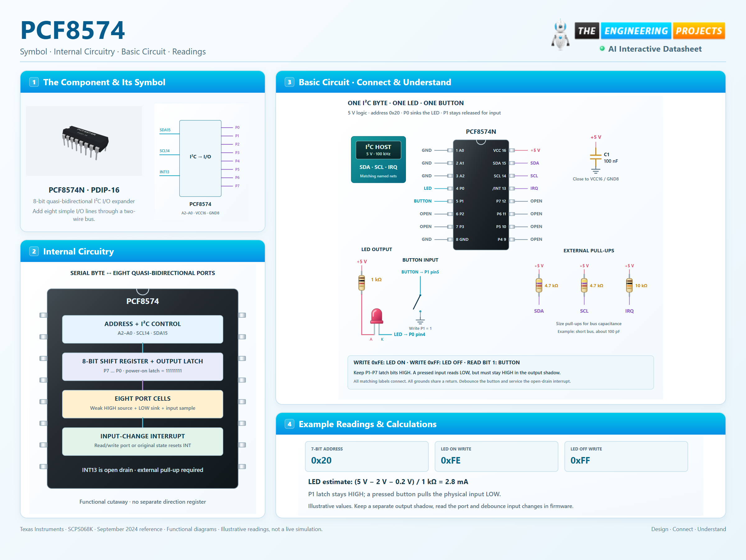
3 stages · Explore one step at a time
Tie A2–A0 to fixed levels. All LOW selects the 7-bit address 0x20.
Send a single port byte. A zero sinks a load, while one releases the line for input or a weak HIGH.
Read the physical port state and service INT. Debounce switches in firmware and preserve input bits in the output shadow.
One output, one input and an interrupt line.
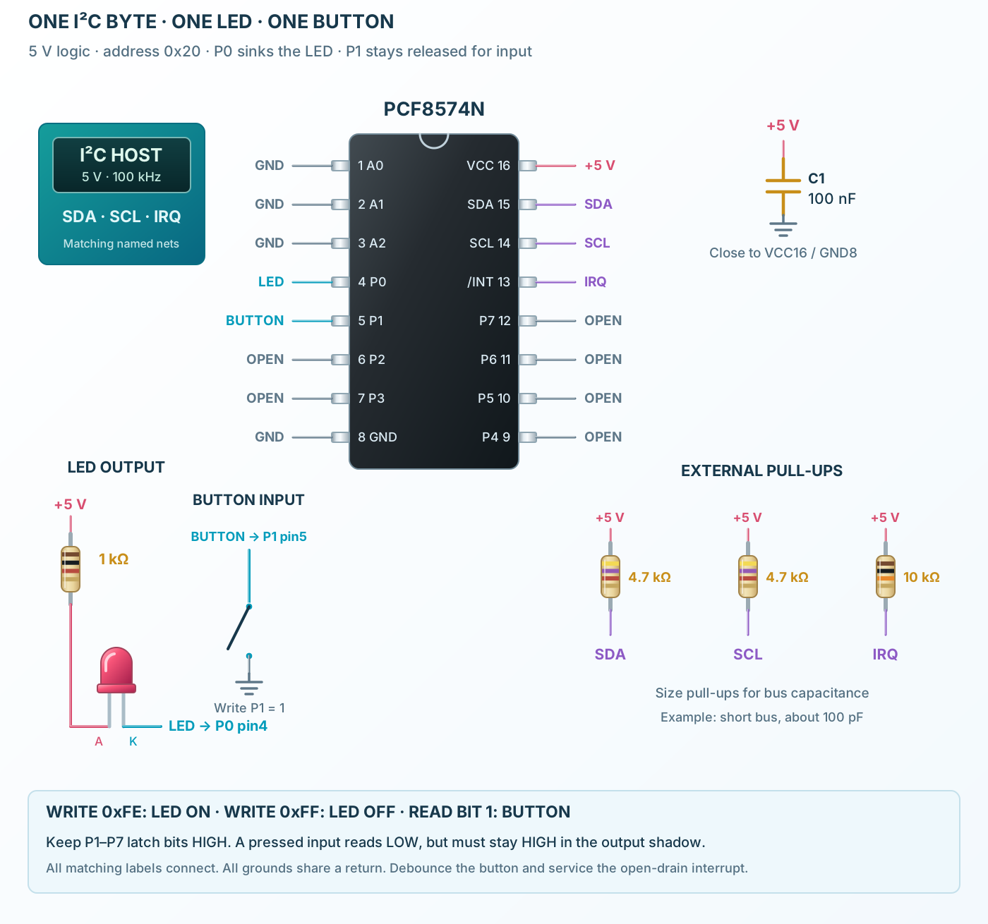
Follow the component values and pin connections
Ground the address pins, use a shared 5 V domain and bypass the supply.
Write FE for the LED on and FF for off; P1 remains HIGH in either write.
Read bit 1 when polling or servicing INT, and debounce in firmware.
I²C control, an 8-bit latch and quasi-bidirectional ports.
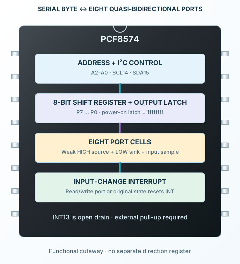
Select a stage to see its role and connections
SDA and SCL move a port byte after the matched address.
LOW activates the sink. HIGH releases a port with weak sourcing for input use.
Reads sample terminal levels; input changes can assert the open-drain interrupt.
Signal names, electrical functions and connection guidance
Scroll within the table to see all columns and rows.
| Pin | Signal | Type | Function & connection |
|---|---|---|---|
| A0 | Address input | Sets bit 0 of the 7-bit I²C address. Tie directly to VCC or GND.Connection guidanceGround all three address inputs for address 0x20. Keep stable throughout a bus transaction. | |
| A1 | Address input | Sets bit 1 of the 7-bit I²C address. Tie directly to VCC or GND.Connection guidanceGround all three address inputs for address 0x20. Keep stable throughout a bus transaction. | |
| A2 | Address input | Sets bit 2 of the 7-bit I²C address. Tie directly to VCC or GND.Connection guidanceGround all three address inputs for address 0x20. Keep stable throughout a bus transaction. | |
| P0 | Quasi-bidirectional I/O | Port bit 0. Writing 0 actively sinks; writing 1 releases the pin with its weak current-source pull-up so it can be read as an input.Connection guidanceConnect LED cathode; LED anode reaches +5 V through 1 kΩ. Not a conventional push-pull HIGH output; preserve input bits as 1 in every output write. | |
| P1 | Quasi-bidirectional I/O | Port bit 1. Writing 0 actively sinks; writing 1 releases the pin with its weak current-source pull-up so it can be read as an input.Connection guidanceConnect a pushbutton to GND and leave its output-latch bit HIGH. Not a conventional push-pull HIGH output; preserve input bits as 1 in every output write. | |
| P2 | Quasi-bidirectional I/O | Port bit 2. Writing 0 actively sinks; writing 1 releases the pin with its weak current-source pull-up so it can be read as an input.Connection guidanceLeave unused pins open with their latch bits HIGH. Not a conventional push-pull HIGH output; preserve input bits as 1 in every output write. | |
| P3 | Quasi-bidirectional I/O | Port bit 3. Writing 0 actively sinks; writing 1 releases the pin with its weak current-source pull-up so it can be read as an input.Connection guidanceLeave unused pins open with their latch bits HIGH. Not a conventional push-pull HIGH output; preserve input bits as 1 in every output write. | |
| GND | Ground | Supply and signal reference.Connection guidanceConnect to controller ground. | |
| P4 | Quasi-bidirectional I/O | Port bit 4. Writing 0 actively sinks; writing 1 releases the pin with its weak current-source pull-up so it can be read as an input.Connection guidanceLeave unused pins open with their latch bits HIGH. Not a conventional push-pull HIGH output; preserve input bits as 1 in every output write. | |
| P5 | Quasi-bidirectional I/O | Port bit 5. Writing 0 actively sinks; writing 1 releases the pin with its weak current-source pull-up so it can be read as an input.Connection guidanceLeave unused pins open with their latch bits HIGH. Not a conventional push-pull HIGH output; preserve input bits as 1 in every output write. | |
| P6 | Quasi-bidirectional I/O | Port bit 6. Writing 0 actively sinks; writing 1 releases the pin with its weak current-source pull-up so it can be read as an input.Connection guidanceLeave unused pins open with their latch bits HIGH. Not a conventional push-pull HIGH output; preserve input bits as 1 in every output write. | |
| P7 | Quasi-bidirectional I/O | Port bit 7. Writing 0 actively sinks; writing 1 releases the pin with its weak current-source pull-up so it can be read as an input.Connection guidanceLeave unused pins open with their latch bits HIGH. Not a conventional push-pull HIGH output; preserve input bits as 1 in every output write. | |
| INT̅ | Open-drain interrupt output | Asserts LOW after a change on an input port. Reading/writing the port or return to its original state resets the interrupt as described in the data sheet.Connection guidancePull up with 10 kΩ to +5 V and connect to a 5 V-compatible interrupt input. Edges during the acknowledge/reset interval may be lost; read the port and debounce buttons. | |
| SCL | I²C clock input | Standard-mode serial clock, up to 100 kHz.Connection guidanceConnect controller SCL with a suitable pull-up to VCC. | |
| SDA | I²C serial data | Bidirectional open-drain serial data.Connection guidanceConnect controller SDA with a suitable pull-up to VCC. | |
| VCC | Positive supply | Operates from 2.5 V to 6 V.Connection guidanceUse +5 V for this example and 100 nF directly to GND pin 8. At 5 V, the specified input HIGH threshold is 3.5 V; do not assume a 3.3 V HIGH is sufficient. |
No pins match these filters. Try another signal name or reset the filters.
Quasi-bidirectional operation
Scroll within the table to see all columns and rows.
| Parameter | Value | Conditions / notes |
|---|---|---|
| Latch bit 0 | Active LOW sink | Suitable for sinking a current-limited LED |
| Latch bit 1 | Weak current-source HIGH | Can be pulled LOW externally and used as input |
| Power-on state | All latch bits HIGH | Pins behave as inputs with weak HIGH sources |
| Direction registers | None | Direction follows the output-latch state |
| Read value | Actual terminal levels | May differ from the software output shadow |
| Output update | Whole 8-bit byte | Keep all input bits HIGH in every write |
No specifications match. Try a parameter name or a unit.
HIGH is not a sustained strong push-pull output. The temporary strong pull-up assists a rising edge only.
7-bit addresses; do not include the R/W bit
Scroll within the table to see all columns and rows.
| Parameter | Value | Conditions / notes |
|---|---|---|
| A2 A1 A0 = 000 | 0x20 | Write byte 0x40 · read byte 0x41 |
| A2 A1 A0 = 001 | 0x21 | Write byte 0x42 · read byte 0x43 |
| A2 A1 A0 = 010 | 0x22 | Write byte 0x44 · read byte 0x45 |
| A2 A1 A0 = 011 | 0x23 | Write byte 0x46 · read byte 0x47 |
| A2 A1 A0 = 100 | 0x24 | Write byte 0x48 · read byte 0x49 |
| A2 A1 A0 = 101 | 0x25 | Write byte 0x4a · read byte 0x4b |
| A2 A1 A0 = 110 | 0x26 | Write byte 0x4c · read byte 0x4d |
| A2 A1 A0 = 111 | 0x27 | Write byte 0x4e · read byte 0x4f |
No specifications match. Try a parameter name or a unit.
PCF8574A has a different address block. This page uses PCF8574.
Address pins grounded · 7-bit address 0x20
Scroll within the table to see all columns and rows.
| Parameter | Value | Conditions / notes |
|---|---|---|
| LED off; inputs released | Write 0xFF | All port latches HIGH |
| LED on at P0 | Write 0xFE | P0 LOW; P1–P7 remain HIGH |
| Read the button | Read one byte; inspect bit 1 | P1 LOW when the grounded button is pressed |
| Typical pressed read with LED on | 0xFC | Assumes other released inputs read HIGH |
| Transfer structure | START → address → data → STOP | No register-address byte |
| INT servicing | Read port, process changes, debounce | Read/write or return to original state can reset INT |
No specifications match. Try a parameter name or a unit.
The example values describe the stated wiring. Do not use a read byte as an unfiltered output-latch shadow.
Recommended operation unless marked otherwise
Scroll within the table to see all columns and rows.
| Parameter | Value | Conditions / notes |
|---|---|---|
| VCC | 2.5–6 V | Example uses 5 V |
| Input HIGH / LOW | ≥ 0.7 VCC / ≤ 0.3 VCC | Supply-dependent logic thresholds |
| P-port weak HIGH source | 30–310 µA magnitude | At VO = GND, VCC 2.5–6 V |
| P-port sink | 10 mA minimum; 25 mA typical | At VCC 5 V, VO 1 V |
| Recommended LOW current | 25 mA maximum per port | Observe total device and thermal limits |
| SDA sink | 3 mA minimum | At VOL 0.4 V |
| INT sink | 1.6 mA minimum | At VOL 0.4 V |
| Standby supply current | 2.5 µA typical; 10 µA maximum | VCC 6 V; inputs at rails; unloaded |
| Operating supply current | 40 µA typical; 100 µA maximum | VCC 6 V; 100 kHz clock; unloaded |
No specifications match. Try a parameter name or a unit.
Do not interpret the absolute 50 mA port rating as a design target.
Standard-mode I²C
Scroll within the table to see all columns and rows.
| Parameter | Value | Conditions / notes |
|---|---|---|
| SCL frequency | 100 kHz maximum | Not a 400 kHz fast-mode expander |
| SCL LOW / HIGH | 4.7 µs / 4.0 µs minimum | Timing requirements |
| SDA setup | 250 ns minimum | Before SCL rises |
| Bus rise time | 1 µs maximum | Choose pull-ups for capacitance and sink current |
| Maximum bus capacitance | 400 pF | Requires a compatible pull-up value |
| Example pull-ups | 4.7 kΩ on SDA and SCL | About 0.40 µs rise at an assumed 100 pF |
| Port / interrupt delay | 4 µs maximum | Specified switching-test conditions |
No specifications match. Try a parameter name or a unit.
The example 4.7 kΩ is a starting value for a short bus, not a guarantee at the full 400 pF limit.
5 V controller and expander
Scroll within the table to see all columns and rows.
| Parameter | Value | Conditions / notes |
|---|---|---|
| Supply | VCC16 +5 V; GND8 common | 100 nF local bypass |
| Address | A0 pin1, A1 pin2, A2 pin3 to GND | Selects 0x20 |
| SDA15 / SCL14 | Controller I²C bus | Each has a 4.7 kΩ pull-up to +5 V |
| INT13 | Controller interrupt input | 10 kΩ pull-up to +5 V |
| P0 pin4 | LED cathode | Anode via 1 kΩ to +5 V; LOW turns it on |
| P1 pin5 | Pushbutton to GND | Write latch bit 1 before reading; debounce |
| P2–P7 | Unused in this example | Leave open and maintain latch bits HIGH |
No specifications match. Try a parameter name or a unit.
At assumed VF 2 V and VOL 0.2 V, LED current is (5 − 2 − 0.2)/1k = 2.8 mA. Actual values depend on the LED and port.
PCF8574N · PDIP-16
Scroll within the table to see all columns and rows.
| Parameter | Value | Conditions / notes |
|---|---|---|
| N package | PDIP-16; 2.54 mm pitch | Through-hole view shown |
| DW package | Wide SOIC-16; 1.27 mm pitch | 7.5 mm nominal body width |
| PW / DGV alternatives | 20 physical leads | Different mapping with unused pins; not shown |
| VCC absolute maximum | 6.5 V | Normal recommended maximum is 6 V |
| Continuous supply/ground current | ±100 mA absolute maximum | Stress rating; sum all loads |
| Storage temperature | −65 to +150°C | Unpowered |
No specifications match. Try a parameter name or a unit.
The two selected 16-pin packages share logical pin numbering but require different PCB footprints.
No matching rowsTry a pin name, parameter, unit or test condition, or reset the filters.
Add low-speed inputs and sinking LED outputs without a direction register.
Manufacturer application guideUse latched outputs for compatible low-rate control lines with suitable buffering where required.
Manufacturer application guideLet the open-drain INT alert the host to an input change, then read and debounce the port.
Manufacturer application guideFind PCF8574 in the Components Library to place its schematic symbol and connect its pins.
Reference page · circuit simulation model not yet availableOpen ProTech