SG3525AAlternating-output PWM controller
Start gently. Switch alternately. Shut down cleanly.
SG3525A is a dual-output PWM controller with an oscillator, error amplifier, pulse-steering flip-flop and source/sink output drivers. Its two outputs alternate, with a LOW off state and an interval in which both are off. External RT, CT and RD set the oscillator period and dead time. A soft-start capacitor limits the initial pulse width, while the shutdown input can terminate a pulse immediately and restart the soft-start sequence after a longer command. This page uses ST SG3525AN and SG3525AP variants. The 12 V scope circuit demonstrates timing, startup and shutdown without a transformer or power MOSFET stage. A complete regulated supply additionally needs feedback, compensation and power-stage protection.
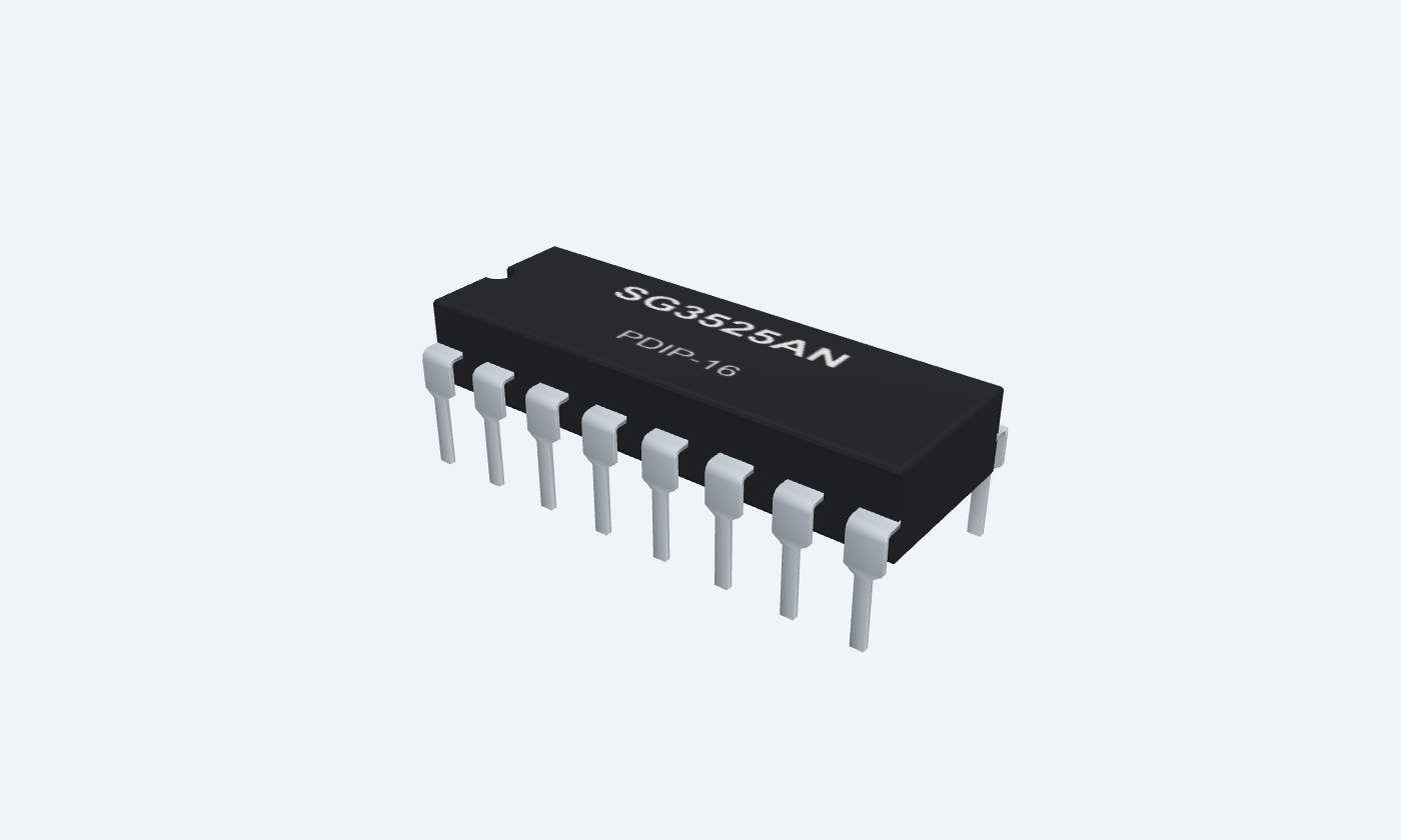
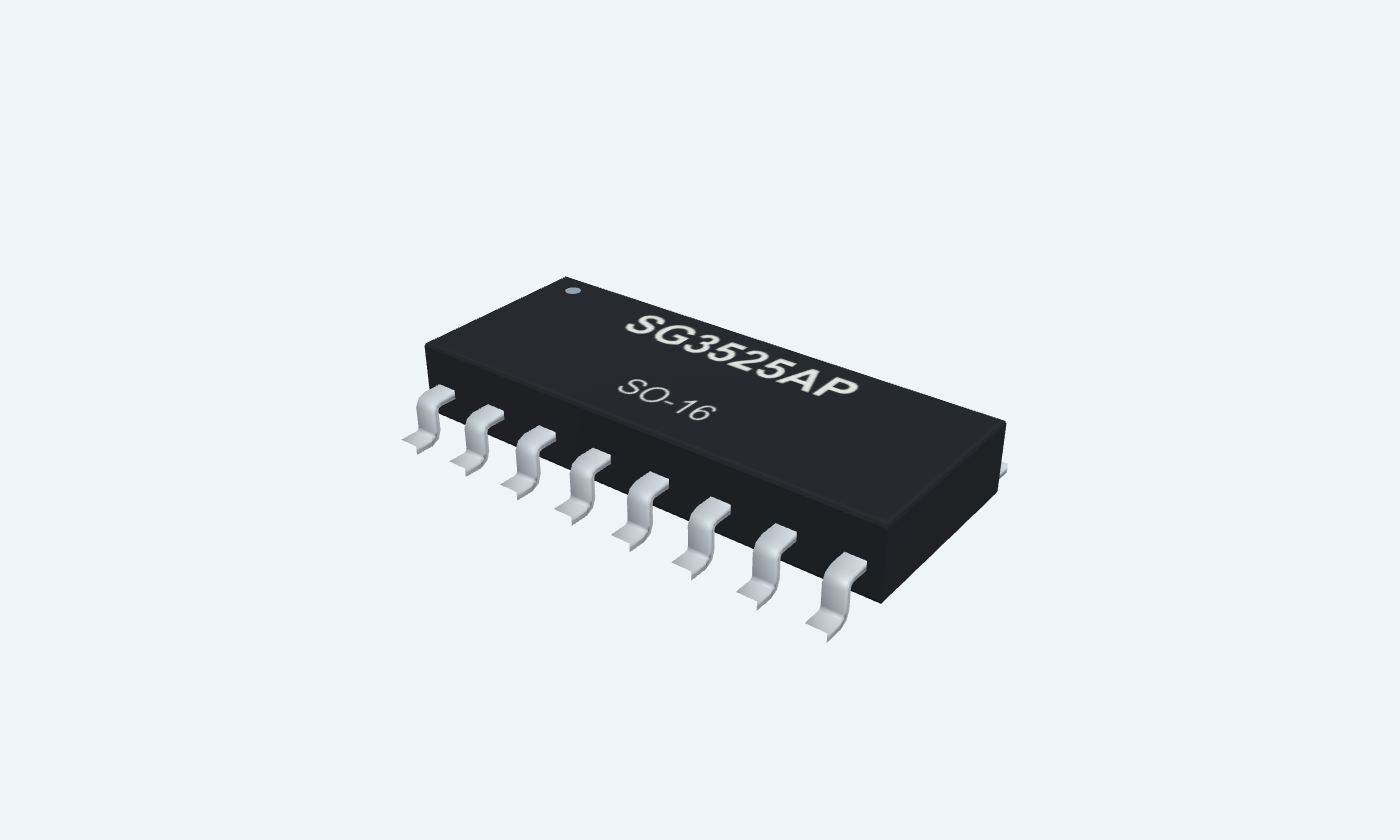

16Physical pins
SG3525ANPDIP-16
Manufacturer-referencedSTMicroelectronics
Pin diagram
Select a pin to explore its connection
Highlight
SG3525ANPDIP-16Top view
SG3525APSO-16Top view
Click a lead or use the arrow keys. Top view
PIN 1 · Error amplifier
Inverting error inputINV
Function
A higher voltage than NI2 reduces the demand for output conduction.
How to connect
Connect to the midpoint of two 10 kΩ resistors from REF16 to GND in this pulse demonstration.
PIN 2 · Error amplifier
Noninverting error inputNI
Function
A higher voltage than INV1 requests a longer pulse.
How to connect
Connect to REF16 for maximum pulse demand in the bench example.
Electrical note
The amplifier inputs are biased in the documented common-mode region, not left floating.
PIN 3 · Timing and protection controls
Oscillator synchronization inputSYNC
Function
External positive clock pulses can synchronize the oscillator.
How to connect
Tie to GND when not using external synchronization.
PIN 4 · Clock and driver outputs
Oscillator clock outputOSC OUT
Function
Clock at the oscillator rate, before alternating output steering.
How to connect
Leave open or use a high-impedance scope.
PIN 5 · RC oscillator
Timing capacitor nodeCT
Function
The oscillator charges and discharges this external capacitor.
How to connect
Connect 10 nF to GND and RD = 100 Ω to DISCHARGE7.
PIN 6 · RC oscillator
Timing resistor nodeRT
Function
Sets the oscillator charging current.
How to connect
Connect 10 kΩ to GND.
PIN 7 · RC oscillator
Timing discharge contactDISCHARGE
Function
The external resistance between this pin and CT sets extra discharge dead time.
How to connect
Connect 100 Ω between pins 7 and 5.
Electrical note
RD belongs between DISCHARGE and CT, not from pin 7 to ground.
PIN 8 · Timing and protection controls
Soft-start capacitor nodeSOFT START
Function
An internal current charges the capacitor and gradually releases the pulse-width limit.
How to connect
Connect 1 µF to GND, positive at pin 8 if polarized.
Electrical note
Shutdown and undervoltage lockout discharge this capacitor.
PIN 9 · Timing and protection controls
Error-amplifier compensationCOMP
Function
Error-amplifier output and PWM control node. External compensation shapes a real regulator loop.
How to connect
Leave externally unconnected for this fixed-demand scope example.
Electrical note
An external pull-down can suppress pulses; do not force a voltage against the amplifier output.
PIN 10 · Timing and protection controls
Active-HIGH shutdownSHUTDOWN
Function
A positive input turns both outputs off; a sustained command discharges soft start.
How to connect
Use 10 kΩ to GND and a normally open pushbutton to REF16.
Electrical note
Do not leave this pin floating.
PIN 11 · Clock and driver outputs
First alternating outputOUT A
Function
Totem-pole output driven from VC13. LOW is the OFF state.
How to connect
Use a high-impedance scope and an optional 10 kΩ load to GND.
PIN 12 · Ground
Common returnGND
Function
Return for the control supply, reference, oscillator and output drivers.
How to connect
Join supply bypass and timing returns close to this pin.
PIN 13 · Supply
Output-driver supplyVC
Function
Separate supply for the two output stages.
How to connect
Connect to +12 V with local 100 nF bypass in the bench circuit.
Electrical note
It is a supply input, not a switch output.
PIN 14 · Clock and driver outputs
Second alternating outputOUT B
Function
Receives alternate oscillator cycles relative to OUT A. LOW is the OFF state.
How to connect
Use the second scope channel and an optional 10 kΩ load to GND.
PIN 15 · Supply
Control supplyVI
Function
Powers the reference and internal control circuitry.
How to connect
Connect +12 V with 100 nF and local bulk decoupling.
PIN 16 · Bias reference
5.1 V referenceVREF
Function
Bias reference for low-current control networks.
How to connect
Bypass with 100 nF; feed NI2, the INV divider and the shutdown switch.
Electrical note
Use the SG3525A electrical table: initial output is specified 5.0–5.2 V.
Key specifications
The oscillator clocks the steering flip-flop. PWM, soft start, shutdown and undervoltage lockout determine whether a pulse reaches an output.
Control supply8–35 V recommended
Nominal reference5.1 V
Recommended oscillator100 Hz–400 kHz See RT / CT / RD limits
SG3525A ambient0–70 °C
Package details
SG3525AN · PDIP-16
| Property | Details |
|---|---|
| Manufacturer | STMicroelectronics |
| Part number | SG3525AN |
| Package | PDIP-16 |
| Connections | 16 pins |
| Mounting | Through-hole |
| Lead pitch | 2.54 mm |
| Package code | PDIP-16 |
| Thermal reference | See operating and package limits |
Recommended operating region
ST SG3525A
Manufacturer specifications 7 parameters
Scroll sideways to see all columns.
| Parameter | Value | Conditions / notes |
|---|---|---|
| Control supply VI | 8–35 V | Pin 15 |
| Driver supply VC | 4.5–35 V | Pin 13; separate driver supply |
| Ambient temperature | 0 to +70°C | SG3525A; do not substitute SG2525A limits |
| Oscillator frequency | 100 Hz–400 kHz | Recommended conditions table |
| Steady output load | 0–100 mA source or sink | Per output; thermal design still applies |
| Peak output load | 0–400 mA | Peak operation only |
| Reference load | 0–20 mA | External control bias |
No specifications match. Try a parameter name or a unit.
The operating table is used here; the front-page frequency headline is broader.
Oscillator and PWM
External components set the rate
Manufacturer specifications 8 parameters
Scroll sideways to see all columns.
| Parameter | Value | Conditions / notes |
|---|---|---|
| RT | 2–150 kΩ | Pin 6 to GND |
| CT | 1–100 nF | Pin 5 to GND |
| RD | 0–500 Ω | Between pins 5 and 7 |
| Frequency equation | fOSC ≈ 1 / [CT × (0.7 RT + 3 RD)] | First-order approximation |
| Output repetition | fA = fB = fOSC / 2 | Alternating cycles |
| Maximum duty per output | 45% minimum capability; 49% typical | Manufacturer test setup |
| PWM zero-duty threshold | 0.7 V minimum; 0.9 V typical | Control threshold, not shutdown-pin threshold |
| PWM maximum-duty threshold | 3.3 V typical; 3.6 V maximum | Specified test conditions |
No specifications match. Try a parameter name or a unit.
Timing tolerances and propagation effects matter; calculated values are not measured guarantees.
Reference and amplifier
Keep bias within the valid region
Manufacturer specifications 6 parameters
Scroll sideways to see all columns.
| Parameter | Value | Conditions / notes |
|---|---|---|
| Initial reference | 5.0–5.2 V; 5.1 V typical | SG3525A at TJ = 25°C |
| Total reference variation | 4.95–5.25 V | Specified line, load and temperature |
| Amplifier offset | 2 mV typical; 10 mV maximum | Specified test conditions |
| Open-loop gain | 75 dB typical; 60 dB minimum | RL ≥ 10 MΩ |
| Common-mode test region | 1.5–5.2 V | Manufacturer rejection-ratio test |
| Example input bias | INV ≈ 2.55 V; NI ≈ 5.1 V | Requests maximum pulse width after soft start |
No specifications match. Try a parameter name or a unit.
Pin 9 is an amplifier output; external forcing must account for its internal drive.
Soft start and shutdown
Two ways to inhibit pulses
Manufacturer specifications 7 parameters
Scroll sideways to see all columns.
| Parameter | Value | Conditions / notes |
|---|---|---|
| Soft-start charging current | 25–80 µA; 50 µA typical | VSD = 0 V, VSS = 0 V |
| Shutdown threshold | 0.6–1.0 V; 0.8 V typical | Output shutdown test at TJ = 25°C |
| Shutdown input current | 0.4 mA typical; 1 mA maximum | VSD = 2.5 V |
| Short shutdown pulse | Terminates the current PWM pulse | May not substantially discharge CSS |
| Long shutdown command | Discharges CSS | Soft start repeats after release |
| UVLO threshold | 6–8 V; 7 V typical | Specified test with COMP and SS HIGH |
| Off state | OUT A = LOW; OUT B = LOW | SG3525A logic |
No specifications match. Try a parameter name or a unit.
Keep shutdown defined. It is not a general-purpose power-stage fault detector without external sensing.
12 V scope circuit
No high-power switching stage
Manufacturer specifications 10 parameters
Scroll sideways to see all columns.
| Parameter | Value | Conditions / notes |
|---|---|---|
| VI15 and VC13 | +12 V | 100 nF at each rail plus local bulk bypass |
| GND12 | Common ground | Short control and bypass returns |
| REF16 | 100 nF bypass | Feeds NI2, shutdown switch and divider |
| INV1 | REF / 2 | Two 10 kΩ divider resistors |
| NI2 / COMP9 | REF / no external connection | Requests full available PWM; soft start still limits startup |
| SYNC3 / OSC OUT4 | GND / open | Free-running oscillator; optional clock probe |
| RT6 / CT5 | 10 kΩ / 10 nF to GND | RD = 100 Ω from CT5 to DISCHARGE7 |
| SOFT START8 | 1 µF to GND | Positive at pin 8 if polarized |
| SHUTDOWN10 | 10 kΩ to GND | Normally open pushbutton connects it to REF16 |
| OUT A11 / OUT B14 | Separate high-impedance scope channels | Optional 10 kΩ load from each output to ground |
No specifications match. Try a parameter name or a unit.
Do not connect outputs together; their active intervals alternate.
Example readings
Nominal calculated values
Manufacturer specifications 7 parameters
Scroll sideways to see all columns.
| Parameter | Value | Conditions / notes |
|---|---|---|
| Oscillator period | 10 nF × (0.7 × 10 kΩ + 3 × 100 Ω) = 73 µs | First-order estimate |
| Oscillator frequency | Approximately 13.70 kHz | Inverse of 73 µs |
| Each output frequency | Approximately 6.85 kHz | Half the oscillator rate |
| Each output period | Approximately 146 µs | Alternating cycle allocation |
| Divider load | 5.1 V / 20 kΩ = 0.255 mA | Nominal reference |
| Soft-start slope | 50 µA / 1 µF = 50 V/s | Typical initial slope |
| Soft-start voltage change | 1 V in about 20 ms | Not a guaranteed complete startup time |
No specifications match. Try a parameter name or a unit.
Real startup also depends on amplifier demand, capacitor tolerance, charging current and PWM thresholds.
Packages and stress limits
SG3525AN · PDIP-16
Manufacturer specifications 7 parameters
Scroll sideways to see all columns.
| Parameter | Value | Conditions / notes |
|---|---|---|
| Through-hole | SG3525AN · DIP16 | 2.54 mm lead pitch |
| Surface mount | SG3525AP · narrow SO16 | 1.27 mm lead pitch |
| VI / VC absolute maximum | 40 V | Stress rating, not normal operating voltage |
| Output absolute maximum | 500 mA | Do not treat as a continuous drive rating |
| Reference absolute maximum | 50 mA | Recommended external load is lower |
| Storage temperature | −65 to +150°C | Unpowered |
| Logic-input absolute range | −0.3 to +5.5 V | Do not apply the 12 V rail to shutdown or sync |
No specifications match. Try a parameter name or a unit.
Footprints are editable starting land patterns; validate clearances and the purchased package before fabrication.
Connections by function
Select a pin for its function, connection guidance and electrical notes.
Error amplifier2 pins
Timing and protection controls4 pins
Clock and driver outputs3 pins
RC oscillator3 pins
Ground1 pin
Supply2 pins
Bias reference1 pin
Error amplifier2 pins
Timing and protection controls4 pins
Clock and driver outputs3 pins
RC oscillator3 pins
Ground1 pin
Supply2 pins
Bias reference1 pin
SG3525A at a glance
Follow the labeled connections and functional stages
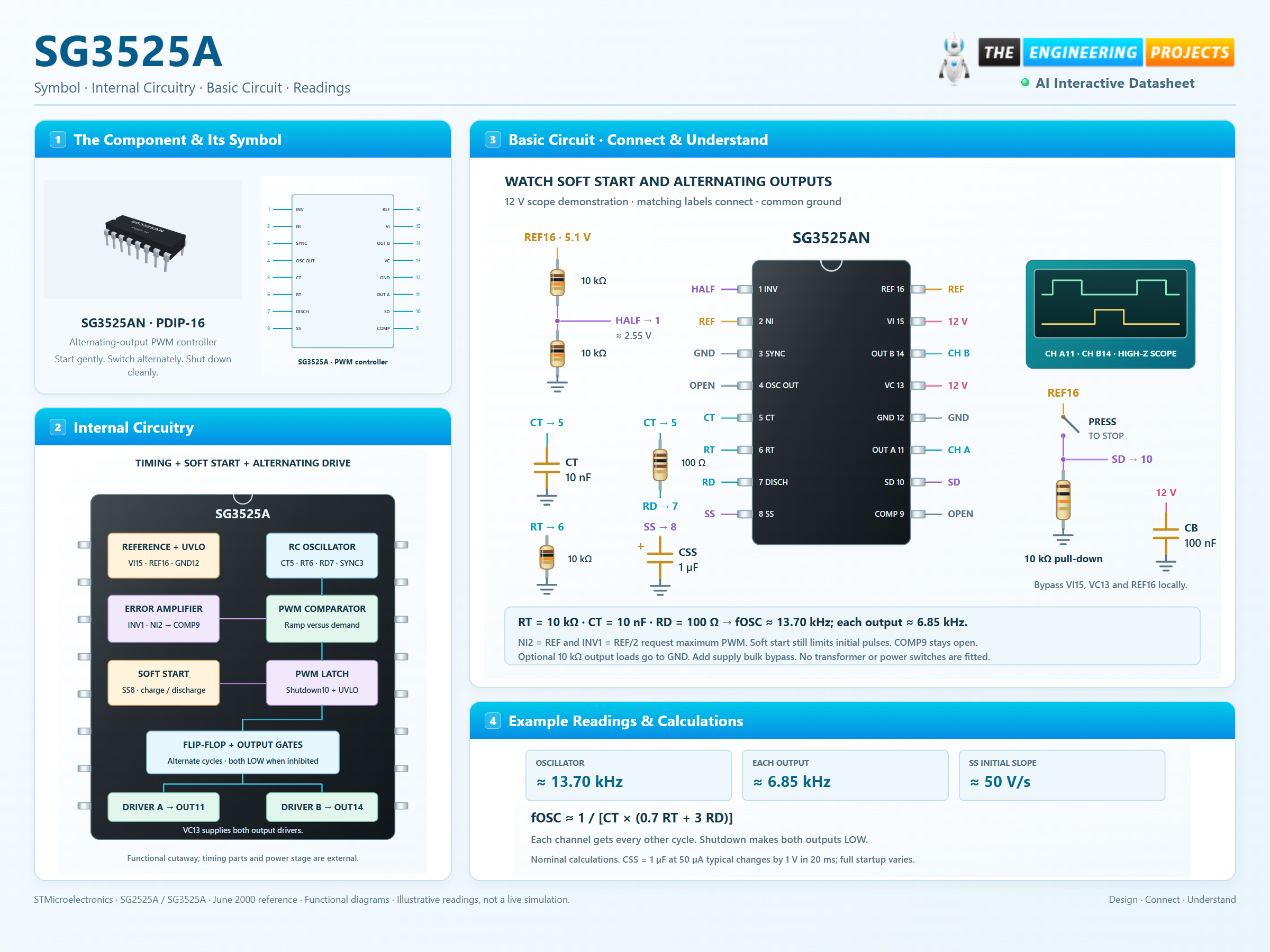
How it works
3 stages · Explore one step at a time
Set the clock and dead time
RT6 and CT5 set the charging interval. RD between pins 5 and 7 lengthens capacitor discharge and the blanking interval.
Release pulses gradually
Soft start limits PWM demand as its capacitor charges. The error amplifier determines the requested conduction after startup.
Steer and protect
Outputs A and B take alternate cycles. Shutdown or undervoltage lockout makes both outputs LOW.
Step 1 of 3
SG3525A in a circuit
A 12 V bench circuit with a shutdown pushbutton.
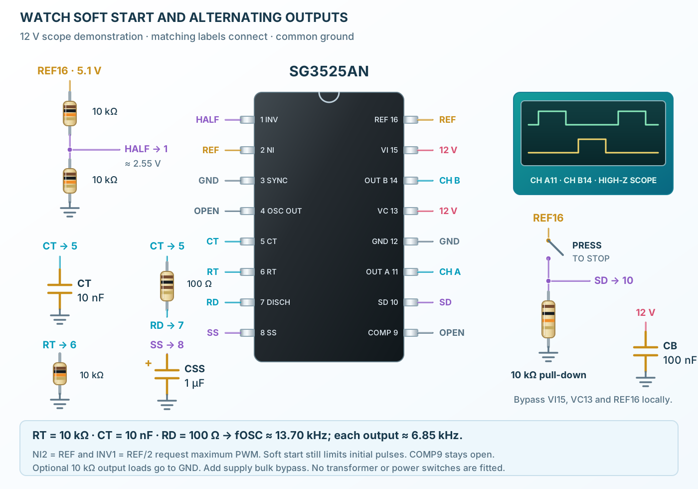
Connect it, step by step
Follow the component values and pin connections
Connect the timing network
CT connects to ground. RD connects CT5 to DISCHARGE7, and RT6 uses its own resistor to ground.
Watch startup
The 1 µF capacitor charges at the internal soft-start current, gradually allowing output pulses.
Press shutdown
The button drives pin 10 HIGH. Holding it discharges soft start; releasing it allows a fresh startup.
Inside SG3525A
Clock, PWM latch and two alternating drivers.
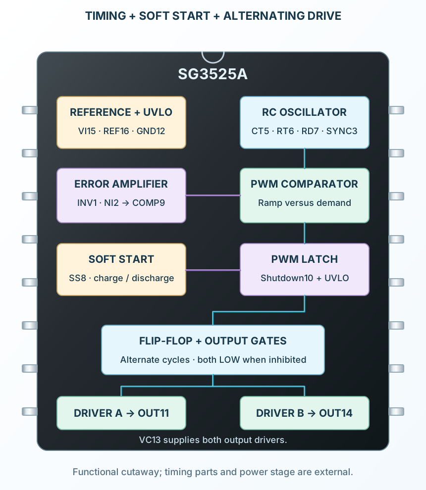
Explore the circuit
Select a stage to see its role and connections
Clock the steering circuit
The oscillator advances the flip-flop so the output channels alternate.
Gate each pulse
PWM demand and soft start control pulse length; shutdown and UVLO override the cycle.
Drive HIGH or LOW
VC powers two totem-pole stages. The off state is LOW.
Selected packagePDIP-16SG3525AN
Physical connections16 pinsPackage-specific numbering
Reference collection8 tables52 parameters & pin functions
Pin reference
Signal names, electrical functions and connection guidance
Physical pin numbers16 pins
Scroll within the table to see all columns and rows.
| Pin | Signal | Type | Function & connection |
|---|---|---|---|
| INV | Inverting error input | A higher voltage than NI2 reduces the demand for output conduction.Connection guidanceConnect to the midpoint of two 10 kΩ resistors from REF16 to GND in this pulse demonstration. | |
| NI | Noninverting error input | A higher voltage than INV1 requests a longer pulse.Connection guidanceConnect to REF16 for maximum pulse demand in the bench example. The amplifier inputs are biased in the documented common-mode region, not left floating. | |
| SYNC | Oscillator synchronization input | External positive clock pulses can synchronize the oscillator.Connection guidanceTie to GND when not using external synchronization. | |
| OSC OUT | Oscillator clock output | Clock at the oscillator rate, before alternating output steering.Connection guidanceLeave open or use a high-impedance scope. | |
| CT | Timing capacitor node | The oscillator charges and discharges this external capacitor.Connection guidanceConnect 10 nF to GND and RD = 100 Ω to DISCHARGE7. | |
| RT | Timing resistor node | Sets the oscillator charging current.Connection guidanceConnect 10 kΩ to GND. | |
| DISCHARGE | Timing discharge contact | The external resistance between this pin and CT sets extra discharge dead time.Connection guidanceConnect 100 Ω between pins 7 and 5. RD belongs between DISCHARGE and CT, not from pin 7 to ground. | |
| SOFT START | Soft-start capacitor node | An internal current charges the capacitor and gradually releases the pulse-width limit.Connection guidanceConnect 1 µF to GND, positive at pin 8 if polarized. Shutdown and undervoltage lockout discharge this capacitor. | |
| COMP | Error-amplifier compensation | Error-amplifier output and PWM control node. External compensation shapes a real regulator loop.Connection guidanceLeave externally unconnected for this fixed-demand scope example. An external pull-down can suppress pulses; do not force a voltage against the amplifier output. | |
| SHUTDOWN | Active-HIGH shutdown | A positive input turns both outputs off; a sustained command discharges soft start.Connection guidanceUse 10 kΩ to GND and a normally open pushbutton to REF16. Do not leave this pin floating. | |
| OUT A | First alternating output | Totem-pole output driven from VC13. LOW is the OFF state.Connection guidanceUse a high-impedance scope and an optional 10 kΩ load to GND. | |
| GND | Common return | Return for the control supply, reference, oscillator and output drivers.Connection guidanceJoin supply bypass and timing returns close to this pin. | |
| VC | Output-driver supply | Separate supply for the two output stages.Connection guidanceConnect to +12 V with local 100 nF bypass in the bench circuit. It is a supply input, not a switch output. | |
| OUT B | Second alternating output | Receives alternate oscillator cycles relative to OUT A. LOW is the OFF state.Connection guidanceUse the second scope channel and an optional 10 kΩ load to GND. | |
| VI | Control supply | Powers the reference and internal control circuitry.Connection guidanceConnect +12 V with 100 nF and local bulk decoupling. | |
| VREF | 5.1 V reference | Bias reference for low-current control networks.Connection guidanceBypass with 100 nF; feed NI2, the INV divider and the shutdown switch. Use the SG3525A electrical table: initial output is specified 5.0–5.2 V. |
No pins match these filters. Try another signal name or reset the filters.
Recommended operating region
ST SG3525A
Manufacturer-referenced values7 parameters
Scroll within the table to see all columns and rows.
| Parameter | Value | Conditions / notes |
|---|---|---|
| Control supply VI | 8–35 V | Pin 15 |
| Driver supply VC | 4.5–35 V | Pin 13; separate driver supply |
| Ambient temperature | 0 to +70°C | SG3525A; do not substitute SG2525A limits |
| Oscillator frequency | 100 Hz–400 kHz | Recommended conditions table |
| Steady output load | 0–100 mA source or sink | Per output; thermal design still applies |
| Peak output load | 0–400 mA | Peak operation only |
| Reference load | 0–20 mA | External control bias |
No specifications match. Try a parameter name or a unit.
The operating table is used here; the front-page frequency headline is broader.
Oscillator and PWM
External components set the rate
Manufacturer-referenced values8 parameters
Scroll within the table to see all columns and rows.
| Parameter | Value | Conditions / notes |
|---|---|---|
| RT | 2–150 kΩ | Pin 6 to GND |
| CT | 1–100 nF | Pin 5 to GND |
| RD | 0–500 Ω | Between pins 5 and 7 |
| Frequency equation | fOSC ≈ 1 / [CT × (0.7 RT + 3 RD)] | First-order approximation |
| Output repetition | fA = fB = fOSC / 2 | Alternating cycles |
| Maximum duty per output | 45% minimum capability; 49% typical | Manufacturer test setup |
| PWM zero-duty threshold | 0.7 V minimum; 0.9 V typical | Control threshold, not shutdown-pin threshold |
| PWM maximum-duty threshold | 3.3 V typical; 3.6 V maximum | Specified test conditions |
No specifications match. Try a parameter name or a unit.
Timing tolerances and propagation effects matter; calculated values are not measured guarantees.
Reference and amplifier
Keep bias within the valid region
Manufacturer-referenced values6 parameters
Scroll within the table to see all columns and rows.
| Parameter | Value | Conditions / notes |
|---|---|---|
| Initial reference | 5.0–5.2 V; 5.1 V typical | SG3525A at TJ = 25°C |
| Total reference variation | 4.95–5.25 V | Specified line, load and temperature |
| Amplifier offset | 2 mV typical; 10 mV maximum | Specified test conditions |
| Open-loop gain | 75 dB typical; 60 dB minimum | RL ≥ 10 MΩ |
| Common-mode test region | 1.5–5.2 V | Manufacturer rejection-ratio test |
| Example input bias | INV ≈ 2.55 V; NI ≈ 5.1 V | Requests maximum pulse width after soft start |
No specifications match. Try a parameter name or a unit.
Pin 9 is an amplifier output; external forcing must account for its internal drive.
Soft start and shutdown
Two ways to inhibit pulses
Manufacturer-referenced values7 parameters
Scroll within the table to see all columns and rows.
| Parameter | Value | Conditions / notes |
|---|---|---|
| Soft-start charging current | 25–80 µA; 50 µA typical | VSD = 0 V, VSS = 0 V |
| Shutdown threshold | 0.6–1.0 V; 0.8 V typical | Output shutdown test at TJ = 25°C |
| Shutdown input current | 0.4 mA typical; 1 mA maximum | VSD = 2.5 V |
| Short shutdown pulse | Terminates the current PWM pulse | May not substantially discharge CSS |
| Long shutdown command | Discharges CSS | Soft start repeats after release |
| UVLO threshold | 6–8 V; 7 V typical | Specified test with COMP and SS HIGH |
| Off state | OUT A = LOW; OUT B = LOW | SG3525A logic |
No specifications match. Try a parameter name or a unit.
Keep shutdown defined. It is not a general-purpose power-stage fault detector without external sensing.
12 V scope circuit
No high-power switching stage
Manufacturer-referenced values10 parameters
Scroll within the table to see all columns and rows.
| Parameter | Value | Conditions / notes |
|---|---|---|
| VI15 and VC13 | +12 V | 100 nF at each rail plus local bulk bypass |
| GND12 | Common ground | Short control and bypass returns |
| REF16 | 100 nF bypass | Feeds NI2, shutdown switch and divider |
| INV1 | REF / 2 | Two 10 kΩ divider resistors |
| NI2 / COMP9 | REF / no external connection | Requests full available PWM; soft start still limits startup |
| SYNC3 / OSC OUT4 | GND / open | Free-running oscillator; optional clock probe |
| RT6 / CT5 | 10 kΩ / 10 nF to GND | RD = 100 Ω from CT5 to DISCHARGE7 |
| SOFT START8 | 1 µF to GND | Positive at pin 8 if polarized |
| SHUTDOWN10 | 10 kΩ to GND | Normally open pushbutton connects it to REF16 |
| OUT A11 / OUT B14 | Separate high-impedance scope channels | Optional 10 kΩ load from each output to ground |
No specifications match. Try a parameter name or a unit.
Do not connect outputs together; their active intervals alternate.
Example readings
Nominal calculated values
Manufacturer-referenced values7 parameters
Scroll within the table to see all columns and rows.
| Parameter | Value | Conditions / notes |
|---|---|---|
| Oscillator period | 10 nF × (0.7 × 10 kΩ + 3 × 100 Ω) = 73 µs | First-order estimate |
| Oscillator frequency | Approximately 13.70 kHz | Inverse of 73 µs |
| Each output frequency | Approximately 6.85 kHz | Half the oscillator rate |
| Each output period | Approximately 146 µs | Alternating cycle allocation |
| Divider load | 5.1 V / 20 kΩ = 0.255 mA | Nominal reference |
| Soft-start slope | 50 µA / 1 µF = 50 V/s | Typical initial slope |
| Soft-start voltage change | 1 V in about 20 ms | Not a guaranteed complete startup time |
No specifications match. Try a parameter name or a unit.
Real startup also depends on amplifier demand, capacitor tolerance, charging current and PWM thresholds.
Packages and stress limits
SG3525AN · PDIP-16
Manufacturer-referenced values7 parameters
Scroll within the table to see all columns and rows.
| Parameter | Value | Conditions / notes |
|---|---|---|
| Through-hole | SG3525AN · DIP16 | 2.54 mm lead pitch |
| Surface mount | SG3525AP · narrow SO16 | 1.27 mm lead pitch |
| VI / VC absolute maximum | 40 V | Stress rating, not normal operating voltage |
| Output absolute maximum | 500 mA | Do not treat as a continuous drive rating |
| Reference absolute maximum | 50 mA | Recommended external load is lower |
| Storage temperature | −65 to +150°C | Unpowered |
| Logic-input absolute range | −0.3 to +5.5 V | Do not apply the 12 V rail to shutdown or sync |
No specifications match. Try a parameter name or a unit.
Footprints are editable starting land patterns; validate clearances and the purchased package before fabrication.
No matching rowsTry a pin name, parameter, unit or test condition, or reset the filters.
Push-pull converter control
Generate alternating drive for a separately designed power stage.
Manufacturer application guideControlled startup
Introduce PWM gradually with an external soft-start capacitor.
Manufacturer application guidePWM timing education
Compare oscillator frequency, individual output frequency and shutdown behavior.
Manufacturer application guideTake it into ProTech
Find SG3525A in the Components Library to place its schematic symbol and connect its pins.
Reference page · circuit simulation model not yet availableOpen ProTech