TB6612FNGDual brushed-DC motor driver
Drive, reverse, brake or coast two small motors.
TB6612FNG contains two MOS H-bridges for brushed DC motors. Each channel has two direction inputs and a PWM input; a shared STBY input disables both channels. The example uses a 5 V motor rail, 3.3 V logic and two small motors. All duplicated motor-output contacts are joined, all three VM pins are powered and every ground contact is connected. Unlike coast, short brake connects both motor terminals LOW. PWM alternates drive and brake when direction inputs are opposite. Check motor stall current and PCB heating before choosing a duty cycle.
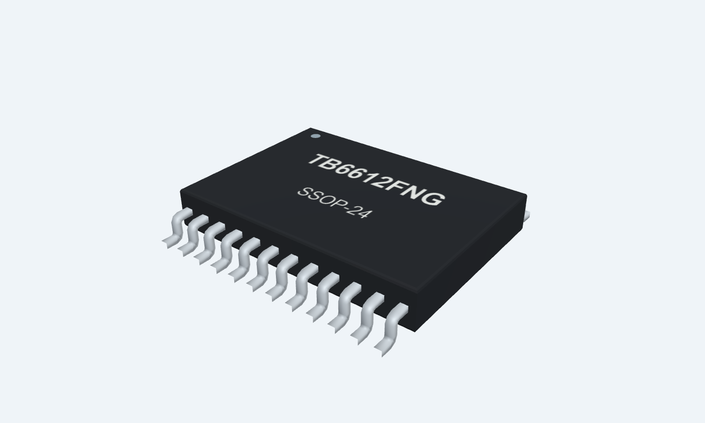

24Physical pins
TB6612FNGSSOP-24
Manufacturer-referencedToshiba
Pin diagram
Select a pin to explore its connection
Highlight
TB6612FNGSSOP-24Top view
Click a lead or use the arrow keys. Top view
PIN 1 · Motor outputs
Motor outputAO1
Function
Physical contact 1 of the AO1 output.
How to connect
Join both AO1 contacts on the PCB; connect the motor between its channel output pairs.
Electrical note
Both motor terminals are switched. Do not ground one motor terminal.
PIN 2 · Motor outputs
Motor outputAO1
Function
Physical contact 2 of the AO1 output.
How to connect
Join both AO1 contacts on the PCB; connect the motor between its channel output pairs.
Electrical note
Both motor terminals are switched. Do not ground one motor terminal.
PIN 3 · Ground
Motor-current returnPGND1
Function
Power ground for the output bridge.
How to connect
Join all four PGND contacts to the supply return with low-impedance copper.
Electrical note
Keep motor-current paths away from small-signal ground routing.
PIN 4 · Ground
Motor-current returnPGND1
Function
Power ground for the output bridge.
How to connect
Join all four PGND contacts to the supply return with low-impedance copper.
Electrical note
Keep motor-current paths away from small-signal ground routing.
PIN 5 · Motor outputs
Motor outputAO2
Function
Physical contact 5 of the AO2 output.
How to connect
Join both AO2 contacts on the PCB; connect the motor between its channel output pairs.
Electrical note
Both motor terminals are switched. Do not ground one motor terminal.
PIN 6 · Motor outputs
Motor outputAO2
Function
Physical contact 6 of the AO2 output.
How to connect
Join both AO2 contacts on the PCB; connect the motor between its channel output pairs.
Electrical note
Both motor terminals are switched. Do not ground one motor terminal.
PIN 7 · Motor outputs
Motor outputBO2
Function
Physical contact 7 of the BO2 output.
How to connect
Join both BO2 contacts on the PCB; connect the motor between its channel output pairs.
Electrical note
Both motor terminals are switched. Do not ground one motor terminal.
PIN 8 · Motor outputs
Motor outputBO2
Function
Physical contact 8 of the BO2 output.
How to connect
Join both BO2 contacts on the PCB; connect the motor between its channel output pairs.
Electrical note
Both motor terminals are switched. Do not ground one motor terminal.
PIN 9 · Ground
Motor-current returnPGND2
Function
Power ground for the output bridge.
How to connect
Join all four PGND contacts to the supply return with low-impedance copper.
Electrical note
Keep motor-current paths away from small-signal ground routing.
PIN 10 · Ground
Motor-current returnPGND2
Function
Power ground for the output bridge.
How to connect
Join all four PGND contacts to the supply return with low-impedance copper.
Electrical note
Keep motor-current paths away from small-signal ground routing.
PIN 11 · Motor outputs
Motor outputBO1
Function
Physical contact 11 of the BO1 output.
How to connect
Join both BO1 contacts on the PCB; connect the motor between its channel output pairs.
Electrical note
Both motor terminals are switched. Do not ground one motor terminal.
PIN 12 · Motor outputs
Motor outputBO1
Function
Physical contact 12 of the BO1 output.
How to connect
Join both BO1 contacts on the PCB; connect the motor between its channel output pairs.
Electrical note
Both motor terminals are switched. Do not ground one motor terminal.
PIN 13 · Supply
Motor supplyVM2
Function
One of three motor-supply contacts.
How to connect
Connect VM1=24, VM2=13 and VM3=14 to the same motor rail.
Electrical note
Operating range 2.5–13.5 V; the 15 V absolute maximum is not a recommended operating voltage.
PIN 14 · Supply
Motor supplyVM3
Function
One of three motor-supply contacts.
How to connect
Connect VM1=24, VM2=13 and VM3=14 to the same motor rail.
Electrical note
Operating range 2.5–13.5 V; the 15 V absolute maximum is not a recommended operating voltage.
PIN 15 · PWM controls
PWM commandPWMB
Function
Duty-cycle input for channel B.
How to connect
Connect to a controller PWM output; use a frequency no higher than 100 kHz.
Electrical note
With opposite direction inputs, PWM LOW selects short brake rather than high-impedance coast.
PIN 16 · Direction controls
Direction commandBIN2
Function
One of the two direction controls for channel B.
How to connect
Use defined HIGH/LOW logic together with PWM and STBY; see the control table.
Electrical note
Internal 200 kΩ pulldown. HIGH requires at least 0.7 × VCC.
PIN 17 · Direction controls
Direction commandBIN1
Function
One of the two direction controls for channel B.
How to connect
Use defined HIGH/LOW logic together with PWM and STBY; see the control table.
Electrical note
Internal 200 kΩ pulldown. HIGH requires at least 0.7 × VCC.
PIN 18 · Ground
Small-signal groundGND
Function
Reference for control inputs and logic supply.
How to connect
Join the common ground while keeping motor return currents out of the control path.
PIN 19 · Standby
Active-LOW standbySTBY
Function
LOW places both channels into standby with high-impedance outputs.
How to connect
Drive HIGH to operate. Keep LOW during initialization.
Electrical note
Internal 200 kΩ pulldown. Standby is not the short-brake mode.
PIN 20 · Supply
Logic supplyVCC
Function
Powers the small-signal control logic.
How to connect
Use the controller logic rail; the example uses 3.3 V. Add local 100 nF and 10 µF bypass.
Electrical note
Operating range 2.7–5.5 V. Input thresholds track VCC.
PIN 21 · Direction controls
Direction commandAIN1
Function
One of the two direction controls for channel A.
How to connect
Use defined HIGH/LOW logic together with PWM and STBY; see the control table.
Electrical note
Internal 200 kΩ pulldown. HIGH requires at least 0.7 × VCC.
PIN 22 · Direction controls
Direction commandAIN2
Function
One of the two direction controls for channel A.
How to connect
Use defined HIGH/LOW logic together with PWM and STBY; see the control table.
Electrical note
Internal 200 kΩ pulldown. HIGH requires at least 0.7 × VCC.
PIN 23 · PWM controls
PWM commandPWMA
Function
Duty-cycle input for channel A.
How to connect
Connect to a controller PWM output; use a frequency no higher than 100 kHz.
Electrical note
With opposite direction inputs, PWM LOW selects short brake rather than high-impedance coast.
PIN 24 · Supply
Motor supplyVM1
Function
One of three motor-supply contacts.
How to connect
Connect VM1=24, VM2=13 and VM3=14 to the same motor rail.
Electrical note
Operating range 2.5–13.5 V; the 15 V absolute maximum is not a recommended operating voltage.
Key specifications
Direction logic selects which MOS switches conduct. PWM alternates drive and short brake; standby releases both outputs. Separate logic and motor rails share a ground reference.
Motor supply2.5–13.5 V operating
Logic supply2.7–5.5 V
PWM ceiling100 kHz
Ambient range−20–85 °C
Package details
TB6612FNG · SSOP-24
| Property | Details |
|---|---|
| Manufacturer | Toshiba |
| Part number | TB6612FNG |
| Package | SSOP-24 |
| Connections | 24 pins |
| Mounting | SMD |
| Lead pitch | 0.65 mm |
| Package code | SSOP-24 |
| Thermal reference | −20°C to +85°C ambient |
Supply and operating limits
Recommended conditions versus absolute ratings
Manufacturer specifications 8 parameters
Scroll sideways to see all columns.
| Parameter | Value | Conditions / notes |
|---|---|---|
| VM motor rail | 2.5–13.5 V | 5 V example; allow margin for regenerated energy |
| VCC logic rail | 2.7–5.5 V | 3.3 V example |
| Output current, no PWM | 1.0 A maximum | Operating table at VM ≥4.5 V |
| Output current, low VM | 0.4 A maximum | Operating table at 2.5 V ≤ VM <4.5 V, without PWM |
| PWM switching | Up to 100 kHz | Use a suitable controller and motor |
| Ambient range | −20°C to +85°C | Derate power as ambient rises |
| Absolute motor / logic supply | 15 V / 6 V | Stress limits, not operating setpoints |
| Absolute current headline | 1.2 A per channel | Thermal and pulse conditions still apply |
No specifications match. Try a parameter name or a unit.
Supply levels, current, duty cycle and PCB thermal design must be considered together.
Input thresholds and current
Control inputs are referenced to VCC
Manufacturer specifications 6 parameters
Scroll sideways to see all columns.
| Parameter | Value | Conditions / notes |
|---|---|---|
| HIGH / LOW thresholds | ≥0.7×VCC / ≤0.3×VCC | At 3.3 V: ≥2.31 V / ≤0.99 V |
| Input pulldowns | 200 kΩ nominal | IN1, IN2, PWM and STBY |
| Logic supply current | 1.1 mA typical; 1.8 mA maximum | VCC=3 V, VM=5 V, STBY=HIGH |
| Standby logic current | 1 µA maximum | STBY=LOW |
| Standby motor-rail current | 1 µA maximum | Specified standby conditions |
| Input HIGH current | 5 / 15 / 25 µA | Minimum / typical / maximum at VIN=3 V |
No specifications match. Try a parameter name or a unit.
A 3.3 V controller is directly compatible when VCC is also 3.3 V.
Direction, brake and standby
Tuple order: IN1 · IN2 · PWM · STBY
Manufacturer specifications 7 parameters
Scroll sideways to see all columns.
| Parameter | Value | Conditions / notes |
|---|---|---|
| HIGH LOW HIGH HIGH | OUT1 HIGH; OUT2 LOW | One drive polarity |
| LOW HIGH HIGH HIGH | OUT1 LOW; OUT2 HIGH | Opposite drive polarity |
| Opposite inputs; PWM LOW; STBY HIGH | Both outputs LOW | Short brake during the PWM off interval |
| HIGH HIGH; PWM either; STBY HIGH | Both outputs LOW | Short brake |
| LOW LOW HIGH HIGH | Both outputs high impedance | Stop / coast |
| Any inputs; STBY LOW | Both outputs high impedance | Standby |
| Other combinations | Use the documented control states | Do not assign behavior from a different driver truth table |
No specifications match. Try a parameter name or a unit.
CW/CCW depends on motor wiring; the electrical polarity is the useful invariant.
Losses and thermal limits
Do not treat a peak-current rating as continuous current
Manufacturer specifications 9 parameters
Scroll sideways to see all columns.
| Parameter | Value | Conditions / notes |
|---|---|---|
| Drive-path drop at 1 A | 0.5 V typical; 0.7 V maximum | VCC=VM=5 V, total upper + lower switches |
| Drive-path drop at 0.3 A | 0.15 V typical; 0.21 V maximum | VCC=VM=5 V |
| One-channel estimate at 1 A | 0.5 W typical conduction | Before switching losses and temperature rise |
| Two-channel estimate at 0.3 A each | 0.09 W typical conduction | 2×0.3 A×0.15 V; illustrative calculation |
| Absolute pulsed current | 2 A, 20 ms, duty ≤20% | Specified continuous-pulse condition |
| Absolute single pulse | 3.2 A, 10 ms | Not a continuous operating value |
| Dissipation at 25°C | 0.78 / 0.89 / 1.36 W | IC only / specified 50×50 mm PCB / specified 76.2×114.3 mm PCB |
| Thermal shutdown / hysteresis | 175°C / 20°C | Design targets, not guaranteed operating temperatures |
| Low-voltage detect / recovery | 1.9 V / 2.2 V | Design-target values |
No specifications match. Try a parameter name or a unit.
Choose motor stall current and protection so normal operation remains within electrical and thermal limits.
Two-motor example
5 V motor supply and 3.3 V controller
Manufacturer specifications 9 parameters
Scroll sideways to see all columns.
| Parameter | Value | Conditions / notes |
|---|---|---|
| Motor A | AO1 pins 1+2; AO2 pins 5+6 | Join each duplicated pair before the motor |
| Motor B | BO1 pins 11+12; BO2 pins 7+8 | Both terminals are driven |
| Motor rail | VM1=24, VM2=13, VM3=14 | Connect all three to 5 V |
| Logic rail | VCC=20 | Connect 3.3 V; controller uses the same level |
| Supply bypass | 10 µF + 100 nF on each rail | Place close to the IC and keep loop area small |
| Ground | PGND1=3+4, PGND2=9+10, GND=18 | Common return with sensible current routing |
| Channel A controls | AIN1=21, AIN2=22, PWMA=23 | Defined controller outputs |
| Channel B controls | BIN1=17, BIN2=16, PWMB=15 | Defined controller outputs |
| Global standby | STBY=19 | Keep LOW until controller initialization is complete |
No specifications match. Try a parameter name or a unit.
Duplicate output pins are physical contacts of the same node, not independently controlled outputs.
SSOP physical package
Bare IC, not a breakout-board header
Manufacturer specifications 7 parameters
Scroll sideways to see all columns.
| Parameter | Value | Conditions / notes |
|---|---|---|
| Package name | SSOP24-P-300-0.65A | Surface mount; 24 gull-wing leads |
| Molded body | 5.6×7.8 mm nominal | Package length may reach 8.3 mm overall |
| Lead pitch / span | 0.65 mm / 7.6 mm nominal | Pin 1 marked by the top-view dot |
| Height | 1.6 mm maximum | Follow seating-plane and assembly tolerances |
| Original copper lands | 1.50×0.40 mm | 7.00 mm row centers; check assembly process |
| Exposed pad | None in this package | Do not add a fictitious center contact |
| Footprint download | KiCad .kicad_mod | Original authored footprint with all 24 pad numbers |
No specifications match. Try a parameter name or a unit.
Mechanical reference: Toshiba package drawing; the download is an original land-pattern interpretation.
Connections by function
Select a pin for its function, connection guidance and electrical notes.
Motor outputs8 pins
Ground5 pins
Supply4 pins
PWM controls2 pins
Direction controls4 pins
Standby1 pin
TB6612FNG at a glance
Follow the labeled connections and functional stages
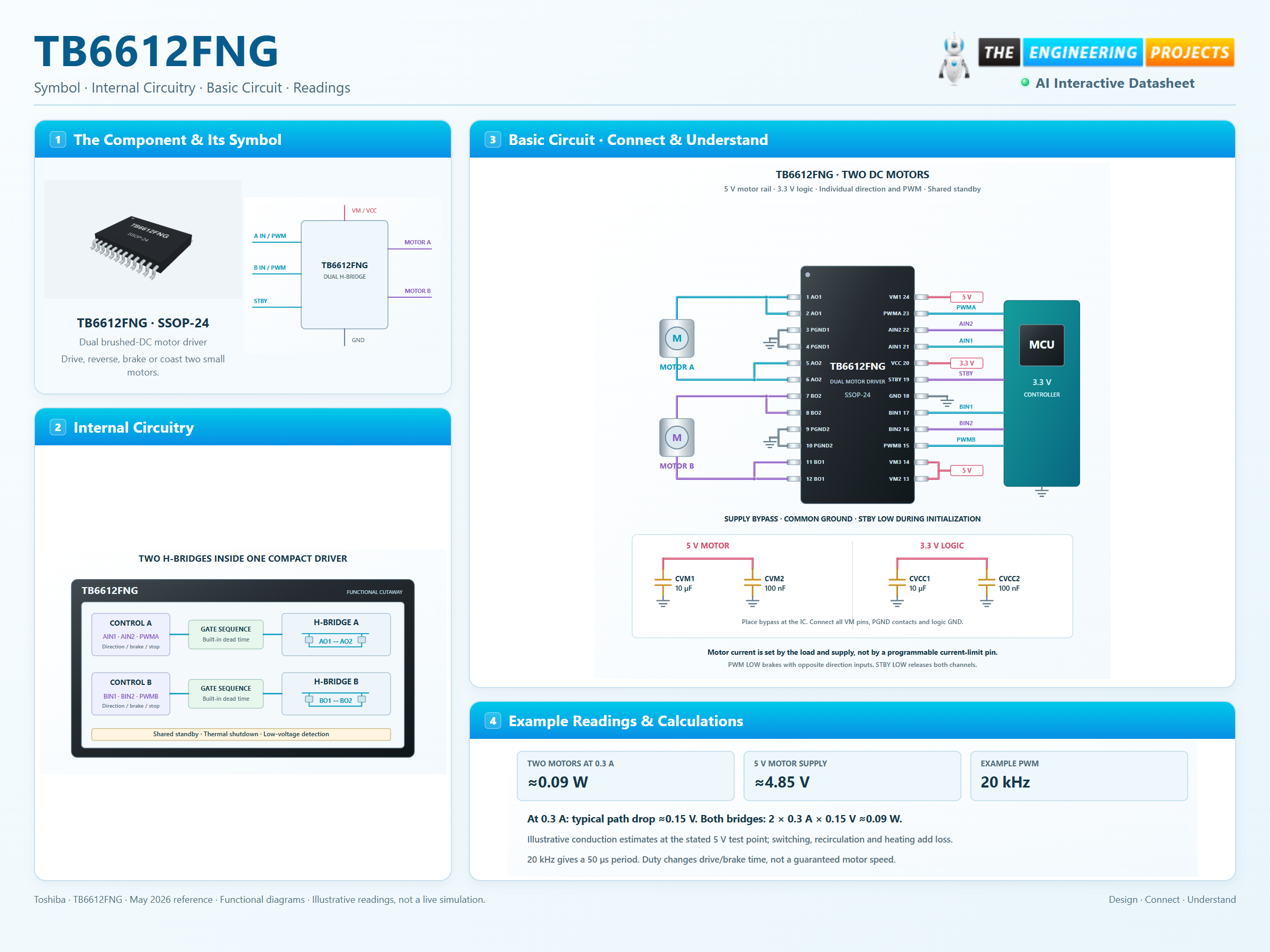
How it works
3 stages · Explore one step at a time
Choose direction
Set opposite IN1/IN2 levels for one direction, then reverse them for the other.
Apply PWM
With STBY HIGH, PWM alternates powered drive and low-side short brake.
Manage current and heat
The motor, supply and switching losses determine current. This IC has no external current-limit adjustment.
Step 1 of 3
TB6612FNG in a circuit
Every physical supply, ground and duplicated output is connected.
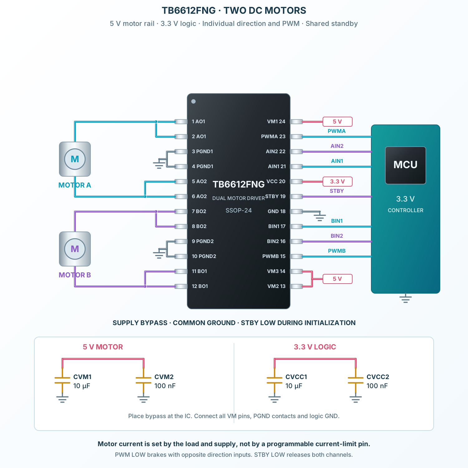
Connect it, step by step
Follow the component values and pin connections
Power both domains
Provide the motor and logic supplies with local bypass.
Join the output pairs
Wire both physical contacts for every motor terminal.
Enable deliberately
Initialize direction and PWM before releasing standby.
Inside TB6612FNG
Two bridges and their control logic inside the package.
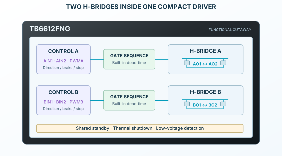
Explore the circuit
Select a stage to see its role and connections
Decode the commands
Each IN pair chooses polarity, brake or stop.
Sequence the switches
Gate control inserts dead time during transitions.
Drive both windings
Power comes from VM; PGND carries bridge return current.
Selected packageSSOP-24TB6612FNG
Physical connections24 pinsPackage-specific numbering
Reference collection7 tables46 parameters & pin functions
Pin reference
Signal names, electrical functions and connection guidance
Physical pin numbers24 pins
Scroll within the table to see all columns and rows.
| Pin | Signal | Type | Function & connection |
|---|---|---|---|
| AO1 | Motor output | Physical contact 1 of the AO1 output.Connection guidanceJoin both AO1 contacts on the PCB; connect the motor between its channel output pairs. Both motor terminals are switched. Do not ground one motor terminal. | |
| AO1 | Motor output | Physical contact 2 of the AO1 output.Connection guidanceJoin both AO1 contacts on the PCB; connect the motor between its channel output pairs. Both motor terminals are switched. Do not ground one motor terminal. | |
| PGND1 | Motor-current return | Power ground for the output bridge.Connection guidanceJoin all four PGND contacts to the supply return with low-impedance copper. Keep motor-current paths away from small-signal ground routing. | |
| PGND1 | Motor-current return | Power ground for the output bridge.Connection guidanceJoin all four PGND contacts to the supply return with low-impedance copper. Keep motor-current paths away from small-signal ground routing. | |
| AO2 | Motor output | Physical contact 5 of the AO2 output.Connection guidanceJoin both AO2 contacts on the PCB; connect the motor between its channel output pairs. Both motor terminals are switched. Do not ground one motor terminal. | |
| AO2 | Motor output | Physical contact 6 of the AO2 output.Connection guidanceJoin both AO2 contacts on the PCB; connect the motor between its channel output pairs. Both motor terminals are switched. Do not ground one motor terminal. | |
| BO2 | Motor output | Physical contact 7 of the BO2 output.Connection guidanceJoin both BO2 contacts on the PCB; connect the motor between its channel output pairs. Both motor terminals are switched. Do not ground one motor terminal. | |
| BO2 | Motor output | Physical contact 8 of the BO2 output.Connection guidanceJoin both BO2 contacts on the PCB; connect the motor between its channel output pairs. Both motor terminals are switched. Do not ground one motor terminal. | |
| PGND2 | Motor-current return | Power ground for the output bridge.Connection guidanceJoin all four PGND contacts to the supply return with low-impedance copper. Keep motor-current paths away from small-signal ground routing. | |
| PGND2 | Motor-current return | Power ground for the output bridge.Connection guidanceJoin all four PGND contacts to the supply return with low-impedance copper. Keep motor-current paths away from small-signal ground routing. | |
| BO1 | Motor output | Physical contact 11 of the BO1 output.Connection guidanceJoin both BO1 contacts on the PCB; connect the motor between its channel output pairs. Both motor terminals are switched. Do not ground one motor terminal. | |
| BO1 | Motor output | Physical contact 12 of the BO1 output.Connection guidanceJoin both BO1 contacts on the PCB; connect the motor between its channel output pairs. Both motor terminals are switched. Do not ground one motor terminal. | |
| VM2 | Motor supply | One of three motor-supply contacts.Connection guidanceConnect VM1=24, VM2=13 and VM3=14 to the same motor rail. Operating range 2.5–13.5 V; the 15 V absolute maximum is not a recommended operating voltage. | |
| VM3 | Motor supply | One of three motor-supply contacts.Connection guidanceConnect VM1=24, VM2=13 and VM3=14 to the same motor rail. Operating range 2.5–13.5 V; the 15 V absolute maximum is not a recommended operating voltage. | |
| PWMB | PWM command | Duty-cycle input for channel B.Connection guidanceConnect to a controller PWM output; use a frequency no higher than 100 kHz. With opposite direction inputs, PWM LOW selects short brake rather than high-impedance coast. | |
| BIN2 | Direction command | One of the two direction controls for channel B.Connection guidanceUse defined HIGH/LOW logic together with PWM and STBY; see the control table. Internal 200 kΩ pulldown. HIGH requires at least 0.7 × VCC. | |
| BIN1 | Direction command | One of the two direction controls for channel B.Connection guidanceUse defined HIGH/LOW logic together with PWM and STBY; see the control table. Internal 200 kΩ pulldown. HIGH requires at least 0.7 × VCC. | |
| GND | Small-signal ground | Reference for control inputs and logic supply.Connection guidanceJoin the common ground while keeping motor return currents out of the control path. | |
| STBY | Active-LOW standby | LOW places both channels into standby with high-impedance outputs.Connection guidanceDrive HIGH to operate. Keep LOW during initialization. Internal 200 kΩ pulldown. Standby is not the short-brake mode. | |
| VCC | Logic supply | Powers the small-signal control logic.Connection guidanceUse the controller logic rail; the example uses 3.3 V. Add local 100 nF and 10 µF bypass. Operating range 2.7–5.5 V. Input thresholds track VCC. | |
| AIN1 | Direction command | One of the two direction controls for channel A.Connection guidanceUse defined HIGH/LOW logic together with PWM and STBY; see the control table. Internal 200 kΩ pulldown. HIGH requires at least 0.7 × VCC. | |
| AIN2 | Direction command | One of the two direction controls for channel A.Connection guidanceUse defined HIGH/LOW logic together with PWM and STBY; see the control table. Internal 200 kΩ pulldown. HIGH requires at least 0.7 × VCC. | |
| PWMA | PWM command | Duty-cycle input for channel A.Connection guidanceConnect to a controller PWM output; use a frequency no higher than 100 kHz. With opposite direction inputs, PWM LOW selects short brake rather than high-impedance coast. | |
| VM1 | Motor supply | One of three motor-supply contacts.Connection guidanceConnect VM1=24, VM2=13 and VM3=14 to the same motor rail. Operating range 2.5–13.5 V; the 15 V absolute maximum is not a recommended operating voltage. |
No pins match these filters. Try another signal name or reset the filters.
Supply and operating limits
Recommended conditions versus absolute ratings
Manufacturer-referenced values8 parameters
Scroll within the table to see all columns and rows.
| Parameter | Value | Conditions / notes |
|---|---|---|
| VM motor rail | 2.5–13.5 V | 5 V example; allow margin for regenerated energy |
| VCC logic rail | 2.7–5.5 V | 3.3 V example |
| Output current, no PWM | 1.0 A maximum | Operating table at VM ≥4.5 V |
| Output current, low VM | 0.4 A maximum | Operating table at 2.5 V ≤ VM <4.5 V, without PWM |
| PWM switching | Up to 100 kHz | Use a suitable controller and motor |
| Ambient range | −20°C to +85°C | Derate power as ambient rises |
| Absolute motor / logic supply | 15 V / 6 V | Stress limits, not operating setpoints |
| Absolute current headline | 1.2 A per channel | Thermal and pulse conditions still apply |
No specifications match. Try a parameter name or a unit.
Supply levels, current, duty cycle and PCB thermal design must be considered together.
Input thresholds and current
Control inputs are referenced to VCC
Manufacturer-referenced values6 parameters
Scroll within the table to see all columns and rows.
| Parameter | Value | Conditions / notes |
|---|---|---|
| HIGH / LOW thresholds | ≥0.7×VCC / ≤0.3×VCC | At 3.3 V: ≥2.31 V / ≤0.99 V |
| Input pulldowns | 200 kΩ nominal | IN1, IN2, PWM and STBY |
| Logic supply current | 1.1 mA typical; 1.8 mA maximum | VCC=3 V, VM=5 V, STBY=HIGH |
| Standby logic current | 1 µA maximum | STBY=LOW |
| Standby motor-rail current | 1 µA maximum | Specified standby conditions |
| Input HIGH current | 5 / 15 / 25 µA | Minimum / typical / maximum at VIN=3 V |
No specifications match. Try a parameter name or a unit.
A 3.3 V controller is directly compatible when VCC is also 3.3 V.
Direction, brake and standby
Tuple order: IN1 · IN2 · PWM · STBY
Manufacturer-referenced values7 parameters
Scroll within the table to see all columns and rows.
| Parameter | Value | Conditions / notes |
|---|---|---|
| HIGH LOW HIGH HIGH | OUT1 HIGH; OUT2 LOW | One drive polarity |
| LOW HIGH HIGH HIGH | OUT1 LOW; OUT2 HIGH | Opposite drive polarity |
| Opposite inputs; PWM LOW; STBY HIGH | Both outputs LOW | Short brake during the PWM off interval |
| HIGH HIGH; PWM either; STBY HIGH | Both outputs LOW | Short brake |
| LOW LOW HIGH HIGH | Both outputs high impedance | Stop / coast |
| Any inputs; STBY LOW | Both outputs high impedance | Standby |
| Other combinations | Use the documented control states | Do not assign behavior from a different driver truth table |
No specifications match. Try a parameter name or a unit.
CW/CCW depends on motor wiring; the electrical polarity is the useful invariant.
Losses and thermal limits
Do not treat a peak-current rating as continuous current
Manufacturer-referenced values9 parameters
Scroll within the table to see all columns and rows.
| Parameter | Value | Conditions / notes |
|---|---|---|
| Drive-path drop at 1 A | 0.5 V typical; 0.7 V maximum | VCC=VM=5 V, total upper + lower switches |
| Drive-path drop at 0.3 A | 0.15 V typical; 0.21 V maximum | VCC=VM=5 V |
| One-channel estimate at 1 A | 0.5 W typical conduction | Before switching losses and temperature rise |
| Two-channel estimate at 0.3 A each | 0.09 W typical conduction | 2×0.3 A×0.15 V; illustrative calculation |
| Absolute pulsed current | 2 A, 20 ms, duty ≤20% | Specified continuous-pulse condition |
| Absolute single pulse | 3.2 A, 10 ms | Not a continuous operating value |
| Dissipation at 25°C | 0.78 / 0.89 / 1.36 W | IC only / specified 50×50 mm PCB / specified 76.2×114.3 mm PCB |
| Thermal shutdown / hysteresis | 175°C / 20°C | Design targets, not guaranteed operating temperatures |
| Low-voltage detect / recovery | 1.9 V / 2.2 V | Design-target values |
No specifications match. Try a parameter name or a unit.
Choose motor stall current and protection so normal operation remains within electrical and thermal limits.
Two-motor example
5 V motor supply and 3.3 V controller
Manufacturer-referenced values9 parameters
Scroll within the table to see all columns and rows.
| Parameter | Value | Conditions / notes |
|---|---|---|
| Motor A | AO1 pins 1+2; AO2 pins 5+6 | Join each duplicated pair before the motor |
| Motor B | BO1 pins 11+12; BO2 pins 7+8 | Both terminals are driven |
| Motor rail | VM1=24, VM2=13, VM3=14 | Connect all three to 5 V |
| Logic rail | VCC=20 | Connect 3.3 V; controller uses the same level |
| Supply bypass | 10 µF + 100 nF on each rail | Place close to the IC and keep loop area small |
| Ground | PGND1=3+4, PGND2=9+10, GND=18 | Common return with sensible current routing |
| Channel A controls | AIN1=21, AIN2=22, PWMA=23 | Defined controller outputs |
| Channel B controls | BIN1=17, BIN2=16, PWMB=15 | Defined controller outputs |
| Global standby | STBY=19 | Keep LOW until controller initialization is complete |
No specifications match. Try a parameter name or a unit.
Duplicate output pins are physical contacts of the same node, not independently controlled outputs.
SSOP physical package
Bare IC, not a breakout-board header
Manufacturer-referenced values7 parameters
Scroll within the table to see all columns and rows.
| Parameter | Value | Conditions / notes |
|---|---|---|
| Package name | SSOP24-P-300-0.65A | Surface mount; 24 gull-wing leads |
| Molded body | 5.6×7.8 mm nominal | Package length may reach 8.3 mm overall |
| Lead pitch / span | 0.65 mm / 7.6 mm nominal | Pin 1 marked by the top-view dot |
| Height | 1.6 mm maximum | Follow seating-plane and assembly tolerances |
| Original copper lands | 1.50×0.40 mm | 7.00 mm row centers; check assembly process |
| Exposed pad | None in this package | Do not add a fictitious center contact |
| Footprint download | KiCad .kicad_mod | Original authored footprint with all 24 pad numbers |
No specifications match. Try a parameter name or a unit.
Mechanical reference: Toshiba package drawing; the download is an original land-pattern interpretation.
No matching rowsTry a pin name, parameter, unit or test condition, or reset the filters.
Two-wheel robots
Command independent left and right drive motors.
Manufacturer application guideSmall actuators
Reverse a motor and choose brake or coast deliberately.
Manufacturer application guidePWM demonstrations
Observe drive/brake intervals without assuming an exact motor speed from duty alone.
Manufacturer application guideTake it into ProTech
Find TB6612FNG in the Components Library to place its schematic symbol and connect its pins.
Reference page · circuit simulation model not yet availableOpen ProTech