Real View
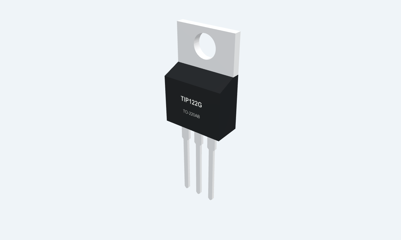
Two transistors. One high-gain load-control stage.
TIP122 is an NPN Darlington power transistor: the first internal transistor drives the base of a second, producing high overall current gain. Both collectors share one terminal, and built-in base-emitter resistors help discharge the internal junctions. The reviewed onsemi TIP122G comes in TO-220AB. Its front-facing leads are base, collector and emitter; the exposed metal tab is electrically connected to collector. This is a low-speed switching and amplifier device, with a larger on-state voltage drop than a single transistor or a suitably driven MOSFET. The headline 5 A and 65 W values are absolute limits under specific conditions. Load current, base drive, safe operating area and cooling must be checked together. The example uses a modest resistive load and clearly labelled voltage assumptions.
Select a pin to explore its connection
Click a lead or use the arrow keys. Front view · B1, C2, E3 · tab = C
Input of the first transistor in the Darlington pair.
Use a current-limiting base resistor and a defined off-state return.
Two base-emitter junctions give a higher on voltage than a single transistor.
Shared collector of the two internal NPN transistors.
Connect to the low side of the controlled load.
The metal tab, shown as contact 4 in the drawing, is also collector. Insulate it from a grounded heatsink where necessary.
Output emitter and circuit return.
Connect to the common control and load ground.
Front view with leads down: B1, C2, E3.
The Darlington connection multiplies current gain, but its two junctions and collector path need more voltage headroom. Check dissipation rather than treating it as an ideal closed switch.
TIP122G · TO-220AB
| Property | Details |
|---|---|
| Manufacturer | onsemi |
| Part number | TIP122G |
| Package | TO-220AB |
| Connections | 3 pins |
| Mounting | Through-hole |
| Lead pitch | 2.54 mm |
| Package code | 221A style 1 |
| Thermal reference | 65 W at case 25°C; 2 W at ambient 25°C |
A reviewed manufacturer reference
Scroll sideways to see all columns.
| Parameter | Value | Conditions / notes |
|---|---|---|
| Selected device | onsemi TIP122G | Pb-free TO-220AB; 50 units per rail |
| Electrical reference | TIP120/D Rev. 10 | June 2024 |
| Package drawing | CASE 221A, style 1 | 2.54 mm lead pitch |
| Front pinout | 1 B · 2 C · 3 E | Tab/contact 4 is collector |
| Construction | Monolithic NPN Darlington | Built-in base-emitter shunt resistors |
| Complementary device | TIP127 | PNP; separate polarity and reference checks apply |
No specifications match. Try a parameter name or a unit.
TIP120 and TIP121 have lower collector-voltage ratings. Do not substitute their limits for TIP122.
Individual stress limits
Scroll sideways to see all columns.
| Parameter | Value | Conditions / notes |
|---|---|---|
| Collector-emitter / collector-base | 100 V / 100 V | VCEO / VCB |
| Emitter-base voltage | 5 V | Reverse stress limit |
| Continuous / peak collector current | 5 A / 8 A | Thermal and pulse constraints apply |
| Base current | 120 mA | Absolute maximum |
| Case-cooled dissipation | 65 W at TC = 25°C | Derate 0.52 W/°C above 25°C |
| Ambient dissipation | 2 W at TA = 25°C | Derate 0.016 W/°C above 25°C |
| Junction / storage range | −65 to +150°C | Absolute range |
No specifications match. Try a parameter name or a unit.
The 65 W rating requires a controlled case temperature; it is not a free-air rating.
Pulsed test points at case 25°C
Scroll sideways to see all columns.
| Parameter | Value | Conditions / notes |
|---|---|---|
| hFE at IC = 0.5 A | 1000 minimum | VCE = 3 V |
| hFE at IC = 3 A | 1000 minimum | VCE = 3 V |
| Typical gain headline | 2500 at IC = 4 A | Typical, not a guaranteed minimum |
| VCE(sat), IC 3 A / IB 12 mA | 2 V maximum | Forced ratio 250 |
| VCE(sat), IC 5 A / IB 20 mA | 4 V maximum | Forced ratio 250 |
| VBE(on) | 2.5 V maximum | IC = 3 A; VCE = 3 V |
No specifications match. Try a parameter name or a unit.
Pulsed tests use pulse width ≤ 300 µs and duty cycle ≤ 2%; do not assume these are thermally steady conditions.
TIP122 conditions from the selected reference
Scroll sideways to see all columns.
| Parameter | Value | Conditions / notes |
|---|---|---|
| ICEO | 0.5 mA maximum | VCE = 50 V; IB = 0 |
| ICBO | 0.2 mA maximum | VCB = 100 V; IE = 0 |
| IEBO | 2 mA maximum | VBE = 5 V; IC = 0 |
| Small-signal current gain | 4 minimum | IC 3 A; VCE 4 V; f 1 MHz |
| Output capacitance | 200 pF maximum | VCB 10 V; IE 0; f 0.1 MHz |
| Switching scope | General-purpose low-speed switching | Storage time depends on base drive and turn-off circuit |
No specifications match. Try a parameter name or a unit.
Leakage and stored charge matter when driving small loads or switching quickly.
Current and voltage must be checked together
Scroll sideways to see all columns.
| Parameter | Value | Conditions / notes |
|---|---|---|
| Junction-to-case resistance | 1.92°C/W maximum | RθJC |
| Junction-to-ambient resistance | 62.5°C/W maximum | RθJA |
| Active-region SOA | Use the manufacturer’s curves | Second breakdown can limit operation before the power rating |
| Pulse operation | Use transient thermal impedance | Pulse width, duty cycle and starting temperature matter |
| Collector tab | Electrically live | Add insulation if the heatsink must be at another potential |
| Flyback clamp | Required for inductive switching | Do not rely on the internal Darlington resistors as a load clamp |
No specifications match. Try a parameter name or a unit.
The example uses a resistor so the circuit can be understood without an inductive switching transient.
Explicit control and load values
Scroll sideways to see all columns.
| Parameter | Value | Conditions / notes |
|---|---|---|
| Load | 100 Ω, at least 2 W | From +12 V to collector pin 2 |
| Base resistor | 1 kΩ from 5 V buffered control | Into base pin 1 |
| Pull-down | 10 kΩ from base to emitter | Defines the external off-state path |
| Emitter pin 3 | Common ground | Control and load return |
| Illustrative junction assumptions | VBE = 1.4 V; VCE = 1.0 V | Not guaranteed manufacturer test points |
| Control-source requirement | Approximately 3.6 mA | Verify the selected controller or buffer |
No specifications match. Try a parameter name or a unit.
Check the actual operating point and thermal margins before choosing a real load.
Nominal illustrative arithmetic
Scroll sideways to see all columns.
| Parameter | Value | Conditions / notes |
|---|---|---|
| Drive-resistor current | 3.60 mA | (5 − 1.4) / 1 kΩ |
| External pull-down current | 0.14 mA | 1.4 / 10 kΩ |
| Device base-terminal current | 3.46 mA | 3.60 − 0.14 mA; internal paths are part of the device |
| Collector current | 110 mA | (12 − 1.0) / 100 Ω |
| Forced current ratio | Approximately 31.8 | 110 / 3.46 |
| Device power | Approximately 0.115 W | 1.0 × 0.110 + 1.4 × 0.00346 |
| Load-resistor loss | 1.21 W | (0.110 A)² × 100 Ω |
No specifications match. Try a parameter name or a unit.
These calculations are teaching values, not measured readings or a timed simulation.
Select a pin for its function, connection guidance and electrical notes.
Follow the labeled connections and functional stages
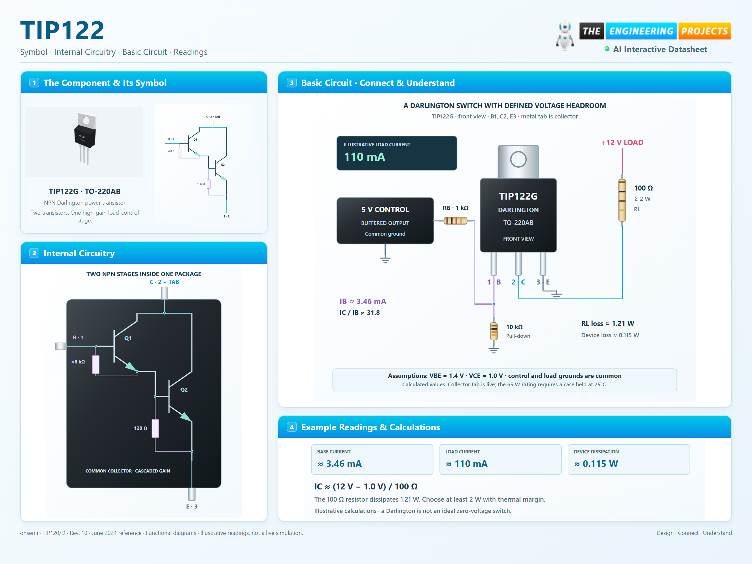
3 stages · Explore one step at a time
The external base current enters the first NPN stage.
Its emitter drives the second stage while both collectors remain common.
A Darlington needs voltage headroom and appropriate cooling.
A modest resistive load makes the current paths explicit.
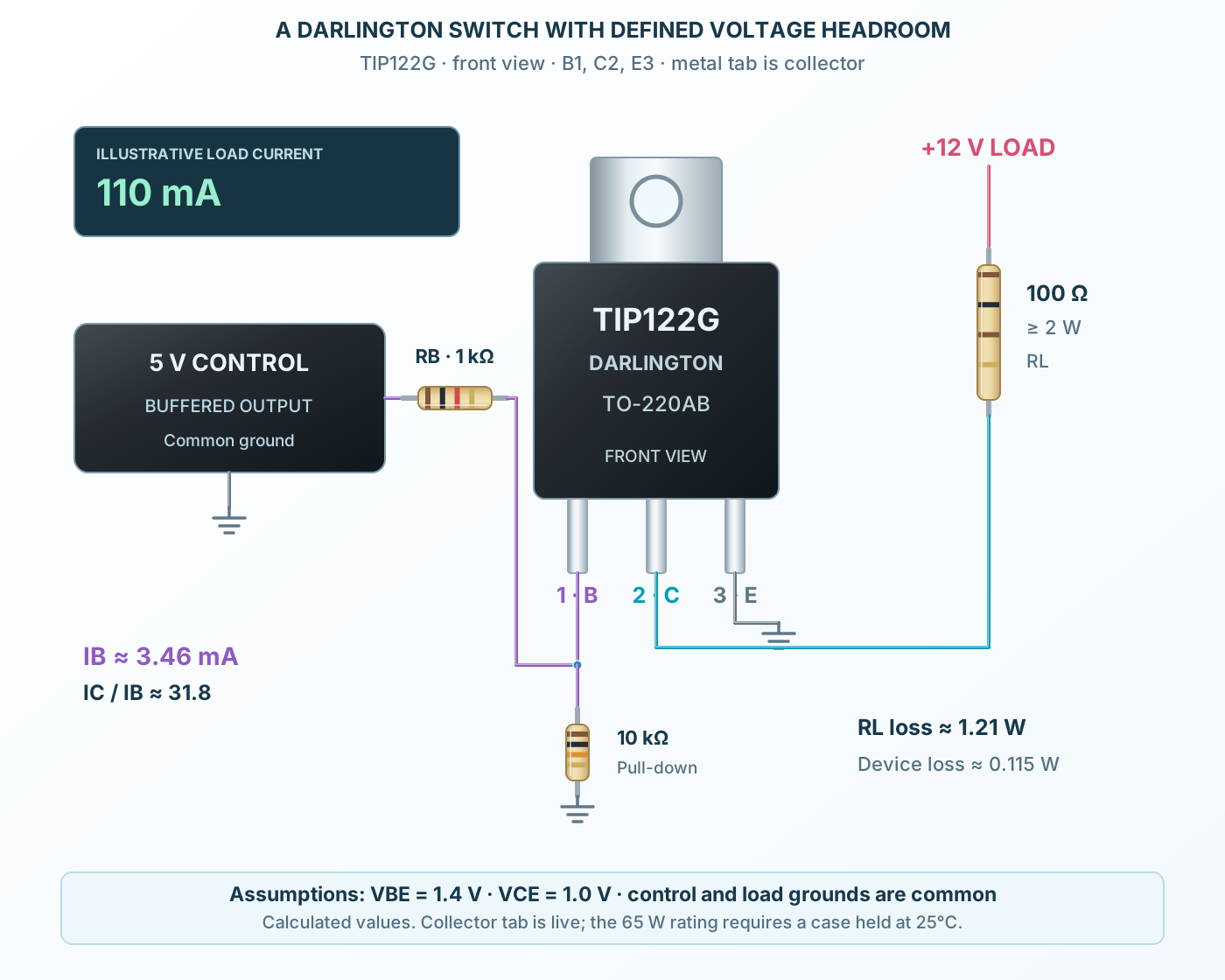
Follow the component values and pin connections
Connect the 100 Ω load to collector pin 2.
Feed base pin 1 through 1 kΩ.
Join emitter pin 3 to the common return.
Two NPN stages, common collector and internal discharge resistors.
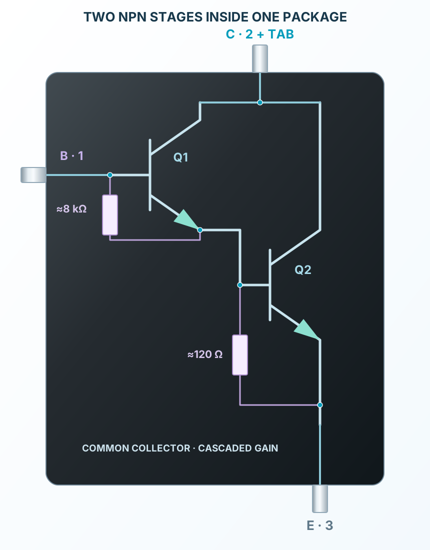
Select a stage to see its role and connections
External base current controls the first NPN.
The first emitter feeds the second base; the collectors are joined.
Approximately 8 kΩ and 120 Ω resistors discharge the internal junctions.
Signal names, electrical functions and connection guidance
Scroll within the table to see all columns and rows.
| Pin | Signal | Type | Function & connection |
|---|---|---|---|
| B | Base | Input of the first transistor in the Darlington pair.Connection guidanceUse a current-limiting base resistor and a defined off-state return. Two base-emitter junctions give a higher on voltage than a single transistor. | |
| C | Collector | Shared collector of the two internal NPN transistors.Connection guidanceConnect to the low side of the controlled load. The metal tab, shown as contact 4 in the drawing, is also collector. Insulate it from a grounded heatsink where necessary. | |
| E | Emitter | Output emitter and circuit return.Connection guidanceConnect to the common control and load ground. Front view with leads down: B1, C2, E3. |
No pins match these filters. Try another signal name or reset the filters.
A reviewed manufacturer reference
Scroll within the table to see all columns and rows.
| Parameter | Value | Conditions / notes |
|---|---|---|
| Selected device | onsemi TIP122G | Pb-free TO-220AB; 50 units per rail |
| Electrical reference | TIP120/D Rev. 10 | June 2024 |
| Package drawing | CASE 221A, style 1 | 2.54 mm lead pitch |
| Front pinout | 1 B · 2 C · 3 E | Tab/contact 4 is collector |
| Construction | Monolithic NPN Darlington | Built-in base-emitter shunt resistors |
| Complementary device | TIP127 | PNP; separate polarity and reference checks apply |
No specifications match. Try a parameter name or a unit.
TIP120 and TIP121 have lower collector-voltage ratings. Do not substitute their limits for TIP122.
Individual stress limits
Scroll within the table to see all columns and rows.
| Parameter | Value | Conditions / notes |
|---|---|---|
| Collector-emitter / collector-base | 100 V / 100 V | VCEO / VCB |
| Emitter-base voltage | 5 V | Reverse stress limit |
| Continuous / peak collector current | 5 A / 8 A | Thermal and pulse constraints apply |
| Base current | 120 mA | Absolute maximum |
| Case-cooled dissipation | 65 W at TC = 25°C | Derate 0.52 W/°C above 25°C |
| Ambient dissipation | 2 W at TA = 25°C | Derate 0.016 W/°C above 25°C |
| Junction / storage range | −65 to +150°C | Absolute range |
No specifications match. Try a parameter name or a unit.
The 65 W rating requires a controlled case temperature; it is not a free-air rating.
Pulsed test points at case 25°C
Scroll within the table to see all columns and rows.
| Parameter | Value | Conditions / notes |
|---|---|---|
| hFE at IC = 0.5 A | 1000 minimum | VCE = 3 V |
| hFE at IC = 3 A | 1000 minimum | VCE = 3 V |
| Typical gain headline | 2500 at IC = 4 A | Typical, not a guaranteed minimum |
| VCE(sat), IC 3 A / IB 12 mA | 2 V maximum | Forced ratio 250 |
| VCE(sat), IC 5 A / IB 20 mA | 4 V maximum | Forced ratio 250 |
| VBE(on) | 2.5 V maximum | IC = 3 A; VCE = 3 V |
No specifications match. Try a parameter name or a unit.
Pulsed tests use pulse width ≤ 300 µs and duty cycle ≤ 2%; do not assume these are thermally steady conditions.
TIP122 conditions from the selected reference
Scroll within the table to see all columns and rows.
| Parameter | Value | Conditions / notes |
|---|---|---|
| ICEO | 0.5 mA maximum | VCE = 50 V; IB = 0 |
| ICBO | 0.2 mA maximum | VCB = 100 V; IE = 0 |
| IEBO | 2 mA maximum | VBE = 5 V; IC = 0 |
| Small-signal current gain | 4 minimum | IC 3 A; VCE 4 V; f 1 MHz |
| Output capacitance | 200 pF maximum | VCB 10 V; IE 0; f 0.1 MHz |
| Switching scope | General-purpose low-speed switching | Storage time depends on base drive and turn-off circuit |
No specifications match. Try a parameter name or a unit.
Leakage and stored charge matter when driving small loads or switching quickly.
Current and voltage must be checked together
Scroll within the table to see all columns and rows.
| Parameter | Value | Conditions / notes |
|---|---|---|
| Junction-to-case resistance | 1.92°C/W maximum | RθJC |
| Junction-to-ambient resistance | 62.5°C/W maximum | RθJA |
| Active-region SOA | Use the manufacturer’s curves | Second breakdown can limit operation before the power rating |
| Pulse operation | Use transient thermal impedance | Pulse width, duty cycle and starting temperature matter |
| Collector tab | Electrically live | Add insulation if the heatsink must be at another potential |
| Flyback clamp | Required for inductive switching | Do not rely on the internal Darlington resistors as a load clamp |
No specifications match. Try a parameter name or a unit.
The example uses a resistor so the circuit can be understood without an inductive switching transient.
Explicit control and load values
Scroll within the table to see all columns and rows.
| Parameter | Value | Conditions / notes |
|---|---|---|
| Load | 100 Ω, at least 2 W | From +12 V to collector pin 2 |
| Base resistor | 1 kΩ from 5 V buffered control | Into base pin 1 |
| Pull-down | 10 kΩ from base to emitter | Defines the external off-state path |
| Emitter pin 3 | Common ground | Control and load return |
| Illustrative junction assumptions | VBE = 1.4 V; VCE = 1.0 V | Not guaranteed manufacturer test points |
| Control-source requirement | Approximately 3.6 mA | Verify the selected controller or buffer |
No specifications match. Try a parameter name or a unit.
Check the actual operating point and thermal margins before choosing a real load.
Nominal illustrative arithmetic
Scroll within the table to see all columns and rows.
| Parameter | Value | Conditions / notes |
|---|---|---|
| Drive-resistor current | 3.60 mA | (5 − 1.4) / 1 kΩ |
| External pull-down current | 0.14 mA | 1.4 / 10 kΩ |
| Device base-terminal current | 3.46 mA | 3.60 − 0.14 mA; internal paths are part of the device |
| Collector current | 110 mA | (12 − 1.0) / 100 Ω |
| Forced current ratio | Approximately 31.8 | 110 / 3.46 |
| Device power | Approximately 0.115 W | 1.0 × 0.110 + 1.4 × 0.00346 |
| Load-resistor loss | 1.21 W | (0.110 A)² × 100 Ω |
No specifications match. Try a parameter name or a unit.
These calculations are teaching values, not measured readings or a timed simulation.
No matching rowsTry a pin name, parameter, unit or test condition, or reset the filters.
Control moderate DC loads with a suitable current and cooling budget.
Manufacturer application guideUse the high gain where the voltage drop is acceptable.
Manufacturer application guideOperate inside the active-region safe operating area.
Manufacturer application guideFind TIP122 in the Components Library to place its schematic symbol and connect its pins.
Reference page · circuit simulation model not yet availableOpen ProTech