Real View
Two transistors. One high-gain load-control stage.
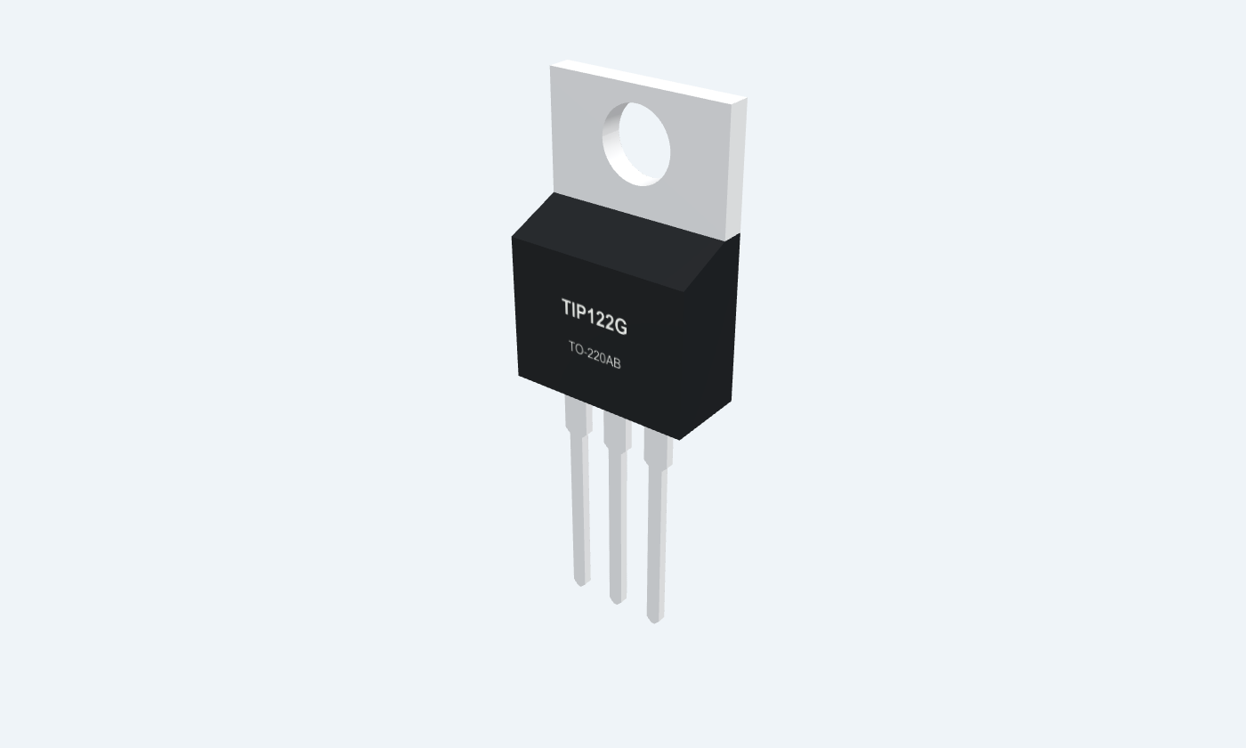
TIP122 is an NPN Darlington power transistor: the first internal transistor drives the base of a second, producing high overall current gain. Both collectors share one terminal, and built-in base-emitter resistors help discharge the internal junctions. The reviewed onsemi TIP122G comes in TO-220AB. Its front-facing leads are base, collector and emitter; the exposed metal tab is electrically connected to collector. This is a low-speed switching and amplifier device, with a larger on-state voltage drop than a single transistor or a suitably driven MOSFET. The headline 5 A and 65 W values are absolute limits under specific conditions. Load current, base drive, safe operating area and cooling must be checked together. The example uses a modest resistive load and clearly labelled voltage assumptions.
Click a lead or use the arrow keys. Front view · B1, C2, E3 · tab = C
Input of the first transistor in the Darlington pair.
Use a current-limiting base resistor and a defined off-state return.
Two base-emitter junctions give a higher on voltage than a single transistor.
Shared collector of the two internal NPN transistors.
Connect to the low side of the controlled load.
The metal tab, shown as contact 4 in the drawing, is also collector. Insulate it from a grounded heatsink where necessary.
Output emitter and circuit return.
Connect to the common control and load ground.
Front view with leads down: B1, C2, E3.
NPN Darlington power transistor
The Darlington connection multiplies current gain, but its two junctions and collector path need more voltage headroom. Check dissipation rather than treating it as an ideal closed switch.
TIP122G
Key parameters and their test conditions
Follows the selected physical package
Select a pin to open its function, electrical notes and wiring guidance.
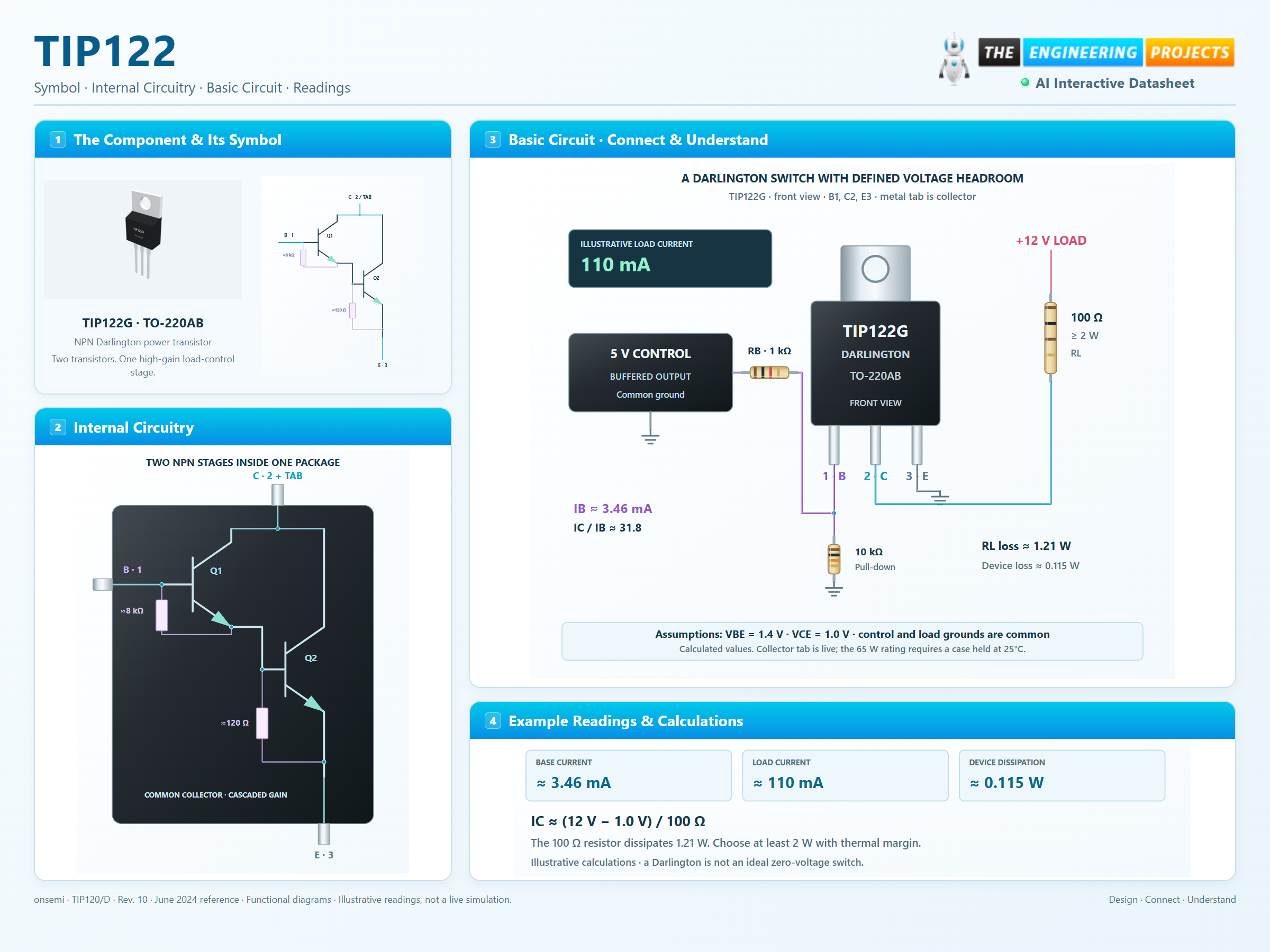
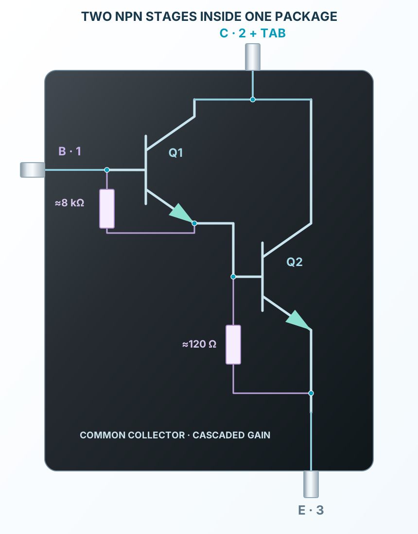
The external base current enters the first NPN stage.
Its emitter drives the second stage while both collectors remain common.
A Darlington needs voltage headroom and appropriate cooling.
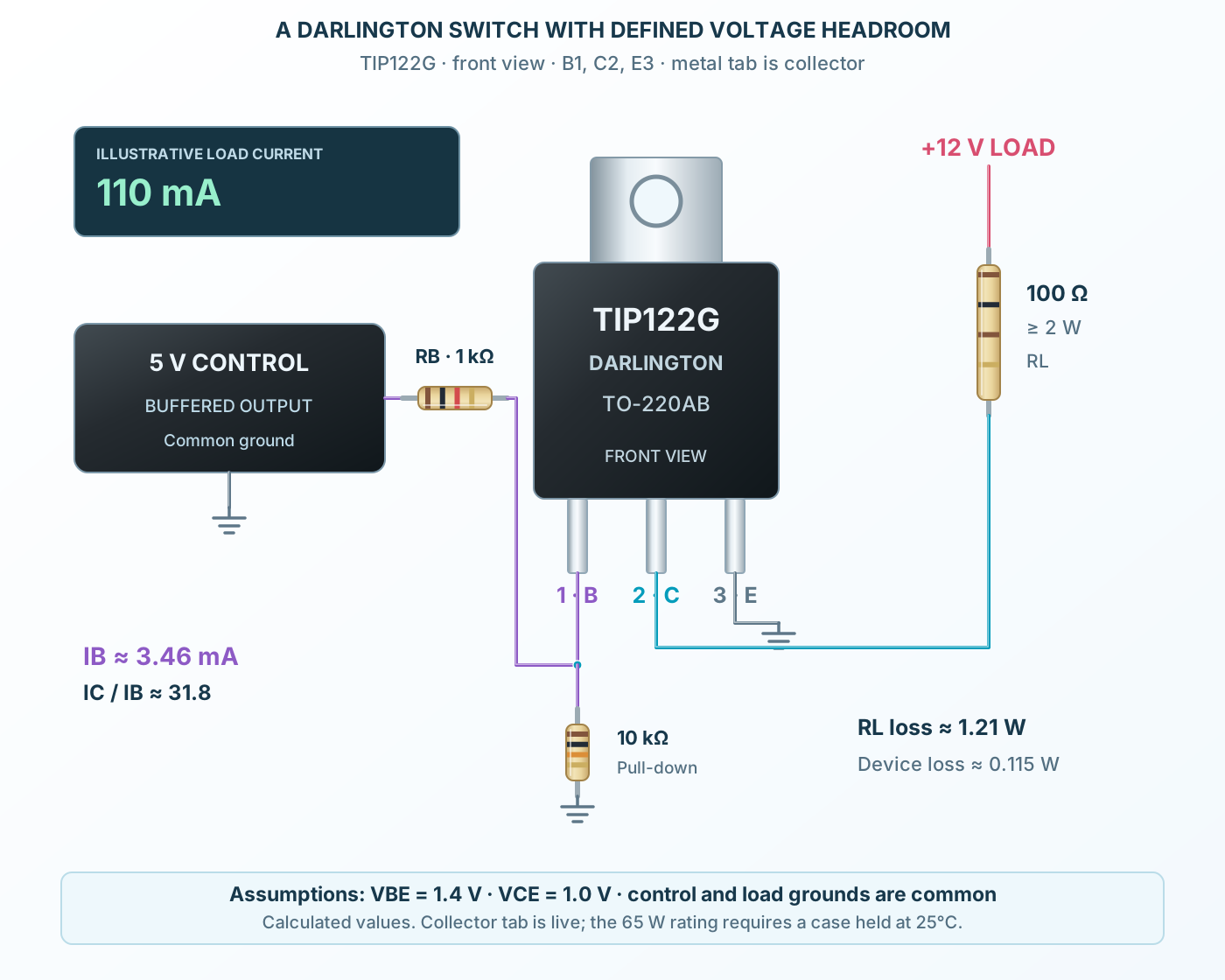
The illustrative 12 V circuit uses a 100 Ω load and assumes 1 V collector-emitter drop. It draws about 110 mA; the transistor loses about 0.115 W including the base contribution.
Select a pin to explore its function and connection.
| Pin | Signal | Type | Function |
|---|---|---|---|
| B | Base | Input of the first transistor in the Darlington pair. | |
| C | Collector | Shared collector of the two internal NPN transistors. | |
| E | Emitter | Output emitter and circuit return. |
No pins match. Try a signal name or choose All pins.
A reviewed manufacturer reference
| Parameter | Value | Conditions / notes |
|---|---|---|
| Selected device | onsemi TIP122G | Pb-free TO-220AB; 50 units per rail |
| Electrical reference | TIP120/D Rev. 10 | June 2024 |
| Package drawing | CASE 221A, style 1 | 2.54 mm lead pitch |
| Front pinout | 1 B · 2 C · 3 E | Tab/contact 4 is collector |
| Construction | Monolithic NPN Darlington | Built-in base-emitter shunt resistors |
| Complementary device | TIP127 | PNP; separate polarity and reference checks apply |
No specifications match. Try a parameter name or a unit.
TIP120 and TIP121 have lower collector-voltage ratings. Do not substitute their limits for TIP122.
Individual stress limits
| Parameter | Value | Conditions / notes |
|---|---|---|
| Collector-emitter / collector-base | 100 V / 100 V | VCEO / VCB |
| Emitter-base voltage | 5 V | Reverse stress limit |
| Continuous / peak collector current | 5 A / 8 A | Thermal and pulse constraints apply |
| Base current | 120 mA | Absolute maximum |
| Case-cooled dissipation | 65 W at TC = 25°C | Derate 0.52 W/°C above 25°C |
| Ambient dissipation | 2 W at TA = 25°C | Derate 0.016 W/°C above 25°C |
| Junction / storage range | −65 to +150°C | Absolute range |
No specifications match. Try a parameter name or a unit.
The 65 W rating requires a controlled case temperature; it is not a free-air rating.
Pulsed test points at case 25°C
| Parameter | Value | Conditions / notes |
|---|---|---|
| hFE at IC = 0.5 A | 1000 minimum | VCE = 3 V |
| hFE at IC = 3 A | 1000 minimum | VCE = 3 V |
| Typical gain headline | 2500 at IC = 4 A | Typical, not a guaranteed minimum |
| VCE(sat), IC 3 A / IB 12 mA | 2 V maximum | Forced ratio 250 |
| VCE(sat), IC 5 A / IB 20 mA | 4 V maximum | Forced ratio 250 |
| VBE(on) | 2.5 V maximum | IC = 3 A; VCE = 3 V |
No specifications match. Try a parameter name or a unit.
Pulsed tests use pulse width ≤ 300 µs and duty cycle ≤ 2%; do not assume these are thermally steady conditions.
TIP122 conditions from the selected reference
| Parameter | Value | Conditions / notes |
|---|---|---|
| ICEO | 0.5 mA maximum | VCE = 50 V; IB = 0 |
| ICBO | 0.2 mA maximum | VCB = 100 V; IE = 0 |
| IEBO | 2 mA maximum | VBE = 5 V; IC = 0 |
| Small-signal current gain | 4 minimum | IC 3 A; VCE 4 V; f 1 MHz |
| Output capacitance | 200 pF maximum | VCB 10 V; IE 0; f 0.1 MHz |
| Switching scope | General-purpose low-speed switching | Storage time depends on base drive and turn-off circuit |
No specifications match. Try a parameter name or a unit.
Leakage and stored charge matter when driving small loads or switching quickly.
Current and voltage must be checked together
| Parameter | Value | Conditions / notes |
|---|---|---|
| Junction-to-case resistance | 1.92°C/W maximum | RθJC |
| Junction-to-ambient resistance | 62.5°C/W maximum | RθJA |
| Active-region SOA | Use the manufacturer’s curves | Second breakdown can limit operation before the power rating |
| Pulse operation | Use transient thermal impedance | Pulse width, duty cycle and starting temperature matter |
| Collector tab | Electrically live | Add insulation if the heatsink must be at another potential |
| Flyback clamp | Required for inductive switching | Do not rely on the internal Darlington resistors as a load clamp |
No specifications match. Try a parameter name or a unit.
The example uses a resistor so the circuit can be understood without an inductive switching transient.
Explicit control and load values
| Parameter | Value | Conditions / notes |
|---|---|---|
| Load | 100 Ω, at least 2 W | From +12 V to collector pin 2 |
| Base resistor | 1 kΩ from 5 V buffered control | Into base pin 1 |
| Pull-down | 10 kΩ from base to emitter | Defines the external off-state path |
| Emitter pin 3 | Common ground | Control and load return |
| Illustrative junction assumptions | VBE = 1.4 V; VCE = 1.0 V | Not guaranteed manufacturer test points |
| Control-source requirement | Approximately 3.6 mA | Verify the selected controller or buffer |
No specifications match. Try a parameter name or a unit.
Check the actual operating point and thermal margins before choosing a real load.
Nominal illustrative arithmetic
| Parameter | Value | Conditions / notes |
|---|---|---|
| Drive-resistor current | 3.60 mA | (5 − 1.4) / 1 kΩ |
| External pull-down current | 0.14 mA | 1.4 / 10 kΩ |
| Device base-terminal current | 3.46 mA | 3.60 − 0.14 mA; internal paths are part of the device |
| Collector current | 110 mA | (12 − 1.0) / 100 Ω |
| Forced current ratio | Approximately 31.8 | 110 / 3.46 |
| Device power | Approximately 0.115 W | 1.0 × 0.110 + 1.4 × 0.00346 |
| Load-resistor loss | 1.21 W | (0.110 A)² × 100 Ω |
No specifications match. Try a parameter name or a unit.
These calculations are teaching values, not measured readings or a timed simulation.
Control moderate DC loads with a suitable current and cooling budget.
Manufacturer application guideUse the high gain where the voltage drop is acceptable.
Manufacturer application guideOperate inside the active-region safe operating area.
Manufacturer application guideFind TIP122 in the Components Library to place its schematic symbol and connect its pins.
Reference page · circuit simulation model not yet availableOpen ProTech