TIP42CPNP power transistor
Control the positive supply. Define the base return.
TIP42C is a 100 V, 6 A PNP bipolar power transistor. Base current controls the load path; allowable operation also depends on collector voltage, pulse duration, cooling and safe operating area. It is a single transistor, not a Darlington. This page follows the archived onsemi TIP42C TO-220 reference, revision 2 of November 2017. With the marked face forward and leads down, the order is base 1, collector 2 and emitter 3. The metal tab is collector. Only this verified through-hole package is offered here. The example uses a 12 V positive-side switch, a 100 Ω resistor load and a source-referenced driver that selects 12 V for off or 7 V for on. The driver sinks base current through 330 Ω; a 10 kΩ base-emitter resistor defines the off state.
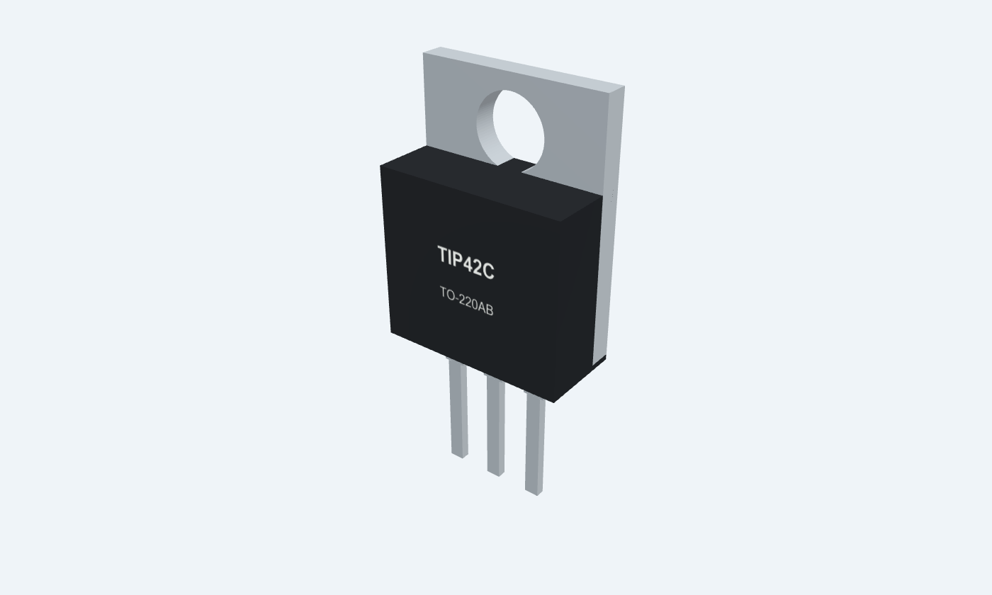

3Physical pins
TIP42CTO-220AB
Manufacturer-referencedonsemi
Pin diagram
Select a pin to explore its connection
Highlight
TIP42CTO-220ABFront view · B1, C2, E3 · tab = C
Click a lead or use the arrow keys. Front view · B1, C2, E3 · tab = C
PIN 1 · Base / drive
BaseB
Function
Current-driven control junction.
How to connect
Use the example’s 330 Ω base resistor and 10 kΩ base-emitter return.
Electrical note
The driver must sink base current. A 3.3 V output cannot directly turn off a 12 V high-side transistor.
PIN 2 · Collector / load
CollectorC
Function
Load terminal, also connected to the metal tab.
How to connect
Connect the 100 Ω resistor load to this terminal.
Electrical note
The exposed tab is electrically live; insulate it when required.
PIN 3 · Supply
EmitterE
Function
Positive supply and base-drive reference.
How to connect
Connect emitter to +12 V. Pull base up to emitter to turn off.
Electrical note
Front view: B1, C2, E3; tab is collector.
Key specifications
The 6 A limit requires adequate base drive and cooling. The saturation test uses 600 mA base current; the 65 W power rating assumes a case held at 25°C.
Collector limit−100 V · absolute VCEO
DC collector limit6 A magnitude · thermal limits apply
DC gain minimum30 IC 0.3 A · VCE 4 V magnitudes
Junction limit150 °C · absolute
Package details
TIP42C · TO-220AB
| Property | Details |
|---|---|
| Manufacturer | onsemi |
| Part number | TIP42C |
| Package | TO-220AB |
| Connections | 3 pins |
| Mounting | Through-hole |
| Lead pitch | 2.54 mm nominal |
| Package code | TO220B03 Rev. 8 |
| Thermal reference | 65 W at case 25°C; 2 W at ambient 25°C |
Device and package scope
Archived manufacturer reference
Manufacturer specifications 5 parameters
Scroll sideways to see all columns.
| Parameter | Value | Conditions / notes |
|---|---|---|
| Selected device | TIP42C · TO-220 | onsemi TIP42C/D Rev. 2, November 2017 |
| Polarity | PNP | Electrical values below are magnitudes |
| Terminals | B1 · C2 · E3 | Metal tab is collector |
| Package drawing | TO220B03 Rev. 8 | Two supplier body shapes are documented |
| Availability | Archived reference | Verify current sourcing separately; no unverified SMD substitute is offered |
No specifications match. Try a parameter name or a unit.
The source is explicitly retained as a legacy reference.
Absolute maximum ratings
Individual stress limits, not operating targets
Manufacturer specifications 5 parameters
Scroll sideways to see all columns.
| Parameter | Value | Conditions / notes |
|---|---|---|
| Collector-emitter / collector-base | 100 / 100 V | C-voltage grade |
| Emitter-base reverse limit | 5 V | Do not overdrive the reverse base junction |
| DC / pulse collector current | 6 / 10 A | Pulse duration and safe operating area apply |
| Base current | 2 A | Absolute maximum |
| Junction maximum | 150°C | Storage −65 to +150°C |
No specifications match. Try a parameter name or a unit.
Thermal limits may restrict current well below the headline rating.
Gain and conduction
25°C; pulse ≤300 µs and duty ≤2%
Manufacturer specifications 5 parameters
Scroll sideways to see all columns.
| Parameter | Value | Conditions / notes |
|---|---|---|
| hFE at IC 0.3 A | 30 minimum | VCE 4 V |
| hFE at IC 3 A | 15–75 | VCE 4 V |
| Collector-emitter saturation | 1.5 V maximum | IC 6 A; IB 600 mA |
| Base-emitter on voltage | 2 V maximum | IC 6 A; VCE 4 V |
| Gain-bandwidth product | 3 MHz minimum | IC 500 mA; VCE 10 V; f 1 MHz |
No specifications match. Try a parameter name or a unit.
PNP voltage and current signs are negative in the manufacturer table; magnitudes are shown here.
Off-state limits
25°C maximum magnitudes
Manufacturer specifications 3 parameters
Scroll sideways to see all columns.
| Parameter | Value | Conditions / notes |
|---|---|---|
| Collector cutoff ICEO | 0.7 mA | VCE 60 V; IB 0 |
| Collector cutoff ICES | 400 µA | VCE 100 V; VEB 0 |
| Emitter cutoff IEBO | 1 mA | VEB 5 V; IC 0 |
No specifications match. Try a parameter name or a unit.
Temperature affects leakage.
Thermal and mechanical reference
Keep the boundary conditions explicit
Manufacturer specifications 6 parameters
Scroll sideways to see all columns.
| Parameter | Value | Conditions / notes |
|---|---|---|
| Collector dissipation | 65 W | Case held at 25°C |
| Ambient dissipation | 2 W | Ambient 25°C |
| Safe operating area | See source curves | Check current, voltage and pulse width together |
| Lead pitch | 2.54 mm nominal | Drawing range 2.40–2.67 mm |
| Lead cross-section maximum | 1.00 × 0.60 mm | Below the stamped shoulder |
| Authored copper / hole | 2.2 / 1.3 mm | Verify fabrication and mechanical clearances |
No specifications match. Try a parameter name or a unit.
The package illustration does not imply a heatsink is present.
12 V resistor-load switch
Explicit illustrative assumptions
Manufacturer specifications 7 parameters
Scroll sideways to see all columns.
| Parameter | Value | Conditions / notes |
|---|---|---|
| Load | 100 Ω, at least 3 W | Collector to ground |
| Base resistor / return | 330 Ω / 10 kΩ | Return resistor goes from base to emitter |
| Buffered driver | 12 V off / 7 V on | Level-shifted; sinks base current |
| Assumed junctions | |VBE| 0.8 V; |VCE| 0.2 V | Teaching assumptions, not guaranteed test points |
| Base current | 12.65 mA | (5−0.8)/330−0.8/10000 |
| Collector current / forced ratio | 118 mA / 9.33 | (12−0.2)/100; IC/IB |
| Transistor / load loss | 33.7 mW / 1.392 W | Include base contribution; allow resistor thermal margin |
No specifications match. Try a parameter name or a unit.
Inductive loads require a suitable clamp and a separate transient check.
Connections by function
Select a pin for its function, connection guidance and electrical notes.
Base / drive1 pin
Collector / load1 pin
Supply1 pin
TIP42C at a glance
Follow the labeled connections and functional stages
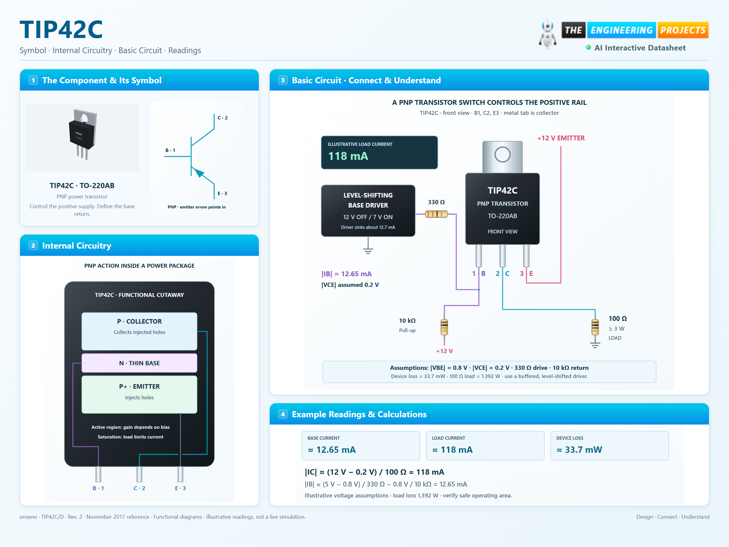
How it works
3 stages · Explore one step at a time
Establish base current
Pull base below emitter through the resistor.
Control the load path
Conventional current flows from emitter to collector.
Release the base charge
The base-emitter return defines off; switching speed depends on drive and stored charge.
Step 1 of 3
TIP42C in a circuit
The supply, driver, load and return are shown explicitly.
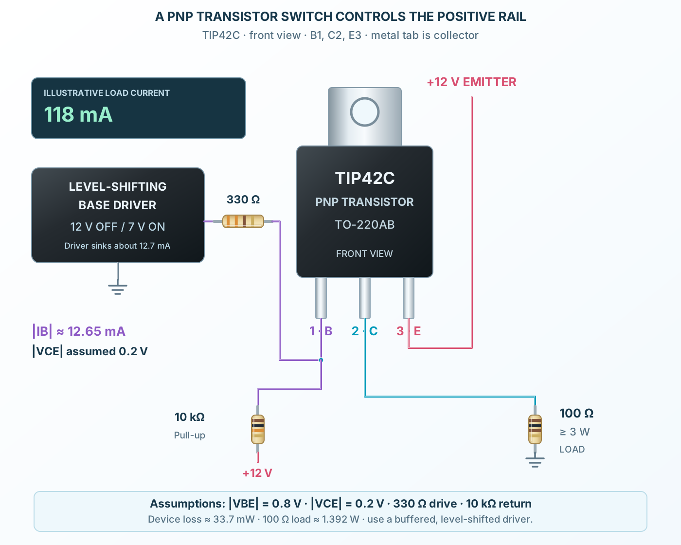
Connect it, step by step
Follow the component values and pin connections
Connect the load
100 Ω from collector to ground.
Drive base deliberately
330 Ω limits drive current; 10 kΩ returns base to emitter.
Check heat
Use at least a 3 W load resistor and check transistor safe operating area.
Inside TIP42C
Three semiconductor regions, two junctions and one controlled current path.
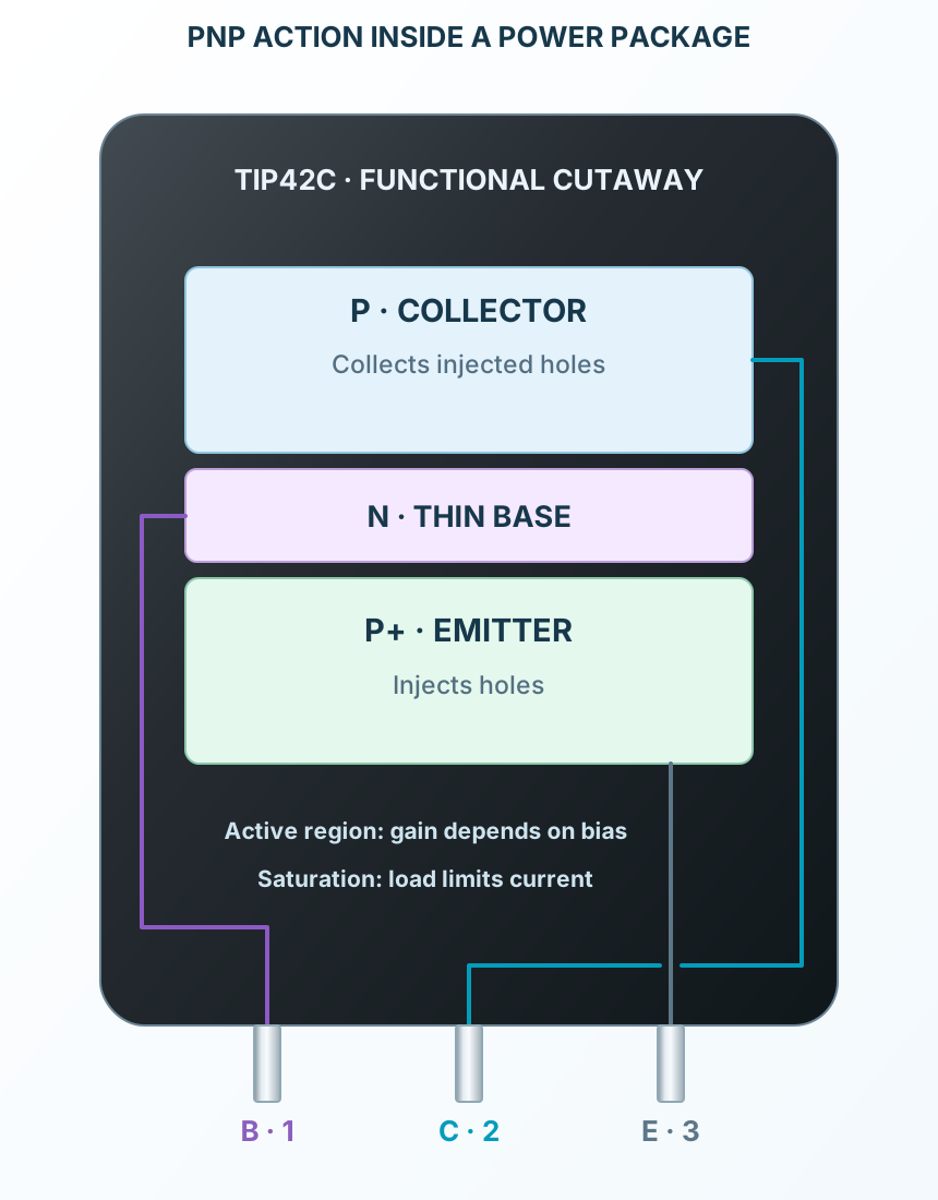
Explore the circuit
Select a stage to see its role and connections
Base junction
The thin base controls carrier transport.
Collector region
The collector supports off-state voltage and carries load current.
Emitter region
The emitter injects carriers when the base junction is forward biased.
Selected packageTO-220ABTIP42C
Physical connections3 pinsPackage-specific numbering
Reference collection7 tables31 parameters & pin functions
Pin reference
Signal names, electrical functions and connection guidance
Physical pin numbers3 pins
Scroll within the table to see all columns and rows.
| Pin | Signal | Type | Function & connection |
|---|---|---|---|
| B | Base | Current-driven control junction.Connection guidanceUse the example’s 330 Ω base resistor and 10 kΩ base-emitter return. The driver must sink base current. A 3.3 V output cannot directly turn off a 12 V high-side transistor. | |
| C | Collector | Load terminal, also connected to the metal tab.Connection guidanceConnect the 100 Ω resistor load to this terminal. The exposed tab is electrically live; insulate it when required. | |
| E | Emitter | Positive supply and base-drive reference.Connection guidanceConnect emitter to +12 V. Pull base up to emitter to turn off. Front view: B1, C2, E3; tab is collector. |
No pins match these filters. Try another signal name or reset the filters.
Device and package scope
Archived manufacturer reference
Manufacturer-referenced values5 parameters
Scroll within the table to see all columns and rows.
| Parameter | Value | Conditions / notes |
|---|---|---|
| Selected device | TIP42C · TO-220 | onsemi TIP42C/D Rev. 2, November 2017 |
| Polarity | PNP | Electrical values below are magnitudes |
| Terminals | B1 · C2 · E3 | Metal tab is collector |
| Package drawing | TO220B03 Rev. 8 | Two supplier body shapes are documented |
| Availability | Archived reference | Verify current sourcing separately; no unverified SMD substitute is offered |
No specifications match. Try a parameter name or a unit.
The source is explicitly retained as a legacy reference.
Absolute maximum ratings
Individual stress limits, not operating targets
Manufacturer-referenced values5 parameters
Scroll within the table to see all columns and rows.
| Parameter | Value | Conditions / notes |
|---|---|---|
| Collector-emitter / collector-base | 100 / 100 V | C-voltage grade |
| Emitter-base reverse limit | 5 V | Do not overdrive the reverse base junction |
| DC / pulse collector current | 6 / 10 A | Pulse duration and safe operating area apply |
| Base current | 2 A | Absolute maximum |
| Junction maximum | 150°C | Storage −65 to +150°C |
No specifications match. Try a parameter name or a unit.
Thermal limits may restrict current well below the headline rating.
Gain and conduction
25°C; pulse ≤300 µs and duty ≤2%
Manufacturer-referenced values5 parameters
Scroll within the table to see all columns and rows.
| Parameter | Value | Conditions / notes |
|---|---|---|
| hFE at IC 0.3 A | 30 minimum | VCE 4 V |
| hFE at IC 3 A | 15–75 | VCE 4 V |
| Collector-emitter saturation | 1.5 V maximum | IC 6 A; IB 600 mA |
| Base-emitter on voltage | 2 V maximum | IC 6 A; VCE 4 V |
| Gain-bandwidth product | 3 MHz minimum | IC 500 mA; VCE 10 V; f 1 MHz |
No specifications match. Try a parameter name or a unit.
PNP voltage and current signs are negative in the manufacturer table; magnitudes are shown here.
Off-state limits
25°C maximum magnitudes
Manufacturer-referenced values3 parameters
Scroll within the table to see all columns and rows.
| Parameter | Value | Conditions / notes |
|---|---|---|
| Collector cutoff ICEO | 0.7 mA | VCE 60 V; IB 0 |
| Collector cutoff ICES | 400 µA | VCE 100 V; VEB 0 |
| Emitter cutoff IEBO | 1 mA | VEB 5 V; IC 0 |
No specifications match. Try a parameter name or a unit.
Temperature affects leakage.
Thermal and mechanical reference
Keep the boundary conditions explicit
Manufacturer-referenced values6 parameters
Scroll within the table to see all columns and rows.
| Parameter | Value | Conditions / notes |
|---|---|---|
| Collector dissipation | 65 W | Case held at 25°C |
| Ambient dissipation | 2 W | Ambient 25°C |
| Safe operating area | See source curves | Check current, voltage and pulse width together |
| Lead pitch | 2.54 mm nominal | Drawing range 2.40–2.67 mm |
| Lead cross-section maximum | 1.00 × 0.60 mm | Below the stamped shoulder |
| Authored copper / hole | 2.2 / 1.3 mm | Verify fabrication and mechanical clearances |
No specifications match. Try a parameter name or a unit.
The package illustration does not imply a heatsink is present.
12 V resistor-load switch
Explicit illustrative assumptions
Manufacturer-referenced values7 parameters
Scroll within the table to see all columns and rows.
| Parameter | Value | Conditions / notes |
|---|---|---|
| Load | 100 Ω, at least 3 W | Collector to ground |
| Base resistor / return | 330 Ω / 10 kΩ | Return resistor goes from base to emitter |
| Buffered driver | 12 V off / 7 V on | Level-shifted; sinks base current |
| Assumed junctions | |VBE| 0.8 V; |VCE| 0.2 V | Teaching assumptions, not guaranteed test points |
| Base current | 12.65 mA | (5−0.8)/330−0.8/10000 |
| Collector current / forced ratio | 118 mA / 9.33 | (12−0.2)/100; IC/IB |
| Transistor / load loss | 33.7 mW / 1.392 W | Include base contribution; allow resistor thermal margin |
No specifications match. Try a parameter name or a unit.
Inductive loads require a suitable clamp and a separate transient check.
No matching rowsTry a pin name, parameter, unit or test condition, or reset the filters.
Load switching
Control modest DC loads with explicit base drive and thermal checks.
Manufacturer application guideAmplifier stages
Use the transistor in its active region within safe operating area.
Manufacturer application guideComplementary stages
Pair NPN and PNP devices with suitable bias and protection.
Manufacturer application guideTake it into ProTech
Find TIP42C in the Components Library to place its schematic symbol and connect its pins.
Reference page · circuit simulation model not yet availableOpen ProTech