TL081Single JFET-input operational amplifier
High input impedance for sensitive analog signals.
TL081 is a single operational amplifier with a JFET input stage and internal frequency compensation. It is useful when the signal source should supply very little input current. The example uses ±15 V rails and a gain of ten. A physical IC, two feedback resistors and local bypass capacitors show how a small input produces a larger output without changing polarity. This reference follows ST’s TL081C grade: TL081CN in DIP-8 and TL081CDT in SO-8. The pins retain the same numbers in both packages; limits from other manufacturers or newer revisions are not mixed into these tables.
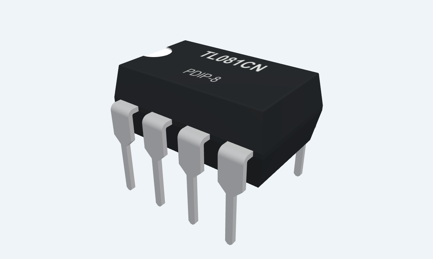
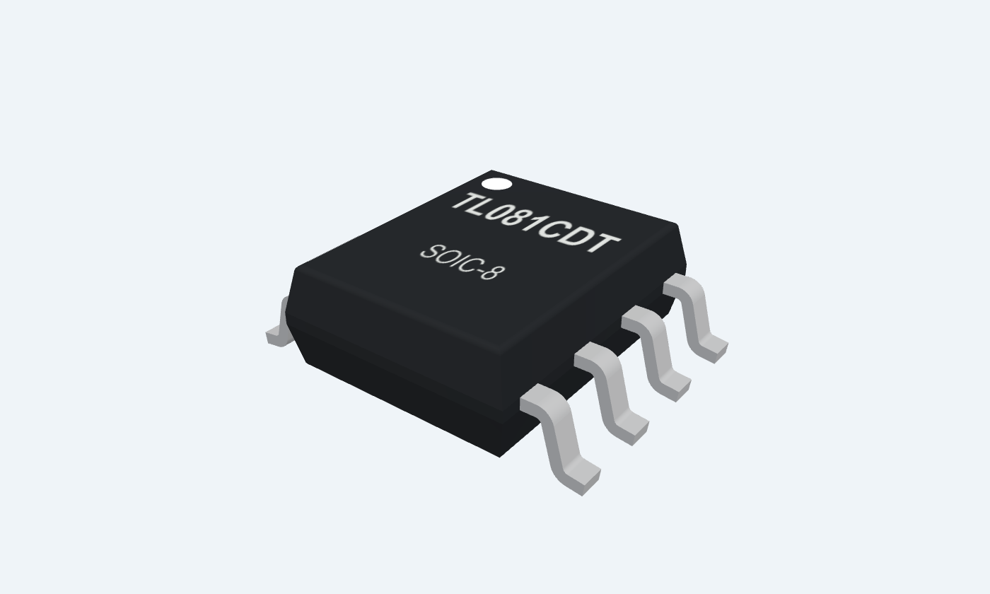

8Physical pins
TL081CNPDIP-8
Manufacturer-referencedSTMicroelectronics
Pin diagram
Select a pin to explore its connection
Highlight
TL081CNPDIP-8Top view
TL081CDTSOIC-8Top view
Click a lead or use the arrow keys. Top view
PIN 1 · Offset trim
Offset nullNULL1
Function
Optional input-offset trim connection.
How to connect
Leave open for the illustrated circuit.
Electrical note
Use the ST offset-adjustment network if trimming is required.
PIN 2 · JFET signal inputs
Inverting inputIN−
Function
Input used by the feedback network.
How to connect
Join the 90 kΩ feedback resistor and 10 kΩ ground resistor.
PIN 3 · JFET signal inputs
Non-inverting inputIN+
Function
JFET signal input.
How to connect
Apply VIN relative to the supply midpoint.
Electrical note
Input bias current increases strongly with temperature.
PIN 4 · Supply
Negative supplyV−
Function
Negative power rail.
How to connect
Connect to −15 V; bypass to signal ground.
PIN 5 · Offset trim
Offset nullNULL2
Function
Second optional trim connection.
How to connect
Leave open in the example.
PIN 6 · Analog output
Analog outputOUT
Function
Output of the internally compensated amplifier.
How to connect
Connect the feedback resistor and a high-impedance meter.
Electrical note
Avoid heavy or capacitive loading without checking stability and output swing.
PIN 7 · Supply
Positive supplyV+
Function
Positive power rail.
How to connect
Connect to +15 V; bypass to signal ground.
PIN 8 · Not connected
No connectionNC
Function
Unused package contact.
How to connect
Leave unconnected.
Key specifications
A JFET input reduces source loading, while external negative feedback determines useful gain.
Supply span6–36 V · total rail-to-rail span
Typical gain-bandwidth4 MHz · specified ±15 V test
C-grade ambient0–70 °C
Typical slew rate16 V/µs · specified test
Package details
TL081CN · PDIP-8
| Property | Details |
|---|---|
| Manufacturer | STMicroelectronics |
| Part number | TL081CN |
| Package | PDIP-8 |
| Connections | 8 pins |
| Mounting | Through-hole |
| Lead pitch | 2.54 mm |
| Package code | dip |
| Thermal reference | Board and package dependent; see manufacturer data |
Operating conditions
ST TL081C grade
Manufacturer specifications 5 parameters
Scroll sideways to see all columns.
| Parameter | Value | Conditions / notes |
|---|---|---|
| Total supply span | 6–36 V | V+ minus V− |
| Ambient temperature | 0 to +70°C | C-grade devices |
| Reference test supply | ±15 V | Used for electrical values unless stated |
| Common-mode range | ±11 V minimum; −12 to +15 V typical | ±15 V supply; see manufacturer conditions |
| Example input | 0.20 V | Relative to the 0 V midpoint |
No specifications match. Try a parameter name or a unit.
A typical range is not a guaranteed operating boundary. Use the specified minimum range for design margin.
DC characteristics
±15 V · 25°C · TL081C
Manufacturer specifications 5 parameters
Scroll sideways to see all columns.
| Parameter | Value | Conditions / notes |
|---|---|---|
| Input offset voltage | 3 mV typical; 10 mV maximum | RS = 50 Ω |
| Input resistance | 1 TΩ typical | Manufacturer Ri characteristic |
| Input offset current | 5 pA typical; 100 pA maximum | Difference between input currents at 25°C |
| No-load supply current | 1.4 mA typical; 2.5 mA maximum | Per amplifier |
| Open-loop gain | 200 V/mV typical; 25 minimum | RL = 2 kΩ; VO = ±10 V |
No specifications match. Try a parameter name or a unit.
Bias leakage rises rapidly with temperature; room-temperature leakage values do not apply over the full range.
Output and dynamic characteristics
±15 V · specified tests
Manufacturer specifications 5 parameters
Scroll sideways to see all columns.
| Parameter | Value | Conditions / notes |
|---|---|---|
| Output swing at RL = 10 kΩ | ±13.5 V typical; ±12 V minimum | 25°C |
| Output swing at RL = 2 kΩ | ±12 V typical; ±10 V minimum | 25°C |
| Gain-bandwidth product | 4 MHz typical; 2.5 MHz minimum | RL = 2 kΩ; CL = 100 pF; f = 100 kHz |
| Slew rate | 16 V/µs typical; 8 V/µs minimum | Unity gain; 10 V input step; RL = 2 kΩ; CL = 100 pF |
| Input noise density | 15 nV/√Hz typical | RS = 100 Ω; 1 kHz |
No specifications match. Try a parameter name or a unit.
Do not infer output current or stability from bandwidth alone.
Gain-of-ten example
Split-supply non-inverting stage
Manufacturer specifications 7 parameters
Scroll sideways to see all columns.
| Parameter | Value | Conditions / notes |
|---|---|---|
| Power rails | +15 V / −15 V | Pins 7 and 4 |
| Input | 0.20 V | IN+ pin 3 |
| Feedback | 90 kΩ | OUT pin 6 to IN− pin 2 |
| Ground resistor | 10 kΩ | IN− pin 2 to 0 V |
| Ideal gain / output | 10 V/V / 2.00 V | 1 + 90 / 10 |
| Bypass | 100 nF per rail | Each rail to the 0 V midpoint |
| Trim and NC | Pins 1, 5, 8 open | No offset-trim network in this circuit |
No specifications match. Try a parameter name or a unit.
The meter is high impedance. Real output includes offset, noise and resistor errors.
Package and pin reference
TL081CN · PDIP-8
Manufacturer specifications 6 parameters
Scroll sideways to see all columns.
| Parameter | Value | Conditions / notes |
|---|---|---|
| Pitch | 2.54 mm | Through-hole |
| Inputs | IN− 2; IN+ 3 | JFET differential pair |
| Output | 6 | Single analog channel |
| Power | V− 4; V+ 7 | 0 V is the external supply midpoint |
| Offset trim | 1 and 5 | Optional; consult the exact manufacturer circuit |
| No connection | 8 | Leave open |
No specifications match. Try a parameter name or a unit.
Do not confuse TL081’s single-amplifier pinout with the dual TL072 pinout.
Connections by function
Select a pin for its function, connection guidance and electrical notes.
Offset trim2 pins
JFET signal inputs2 pins
Supply2 pins
Analog output1 pin
Not connected1 pin
Offset trim2 pins
JFET signal inputs2 pins
Supply2 pins
Analog output1 pin
Not connected1 pin
TL081 at a glance
Follow the labeled connections and functional stages
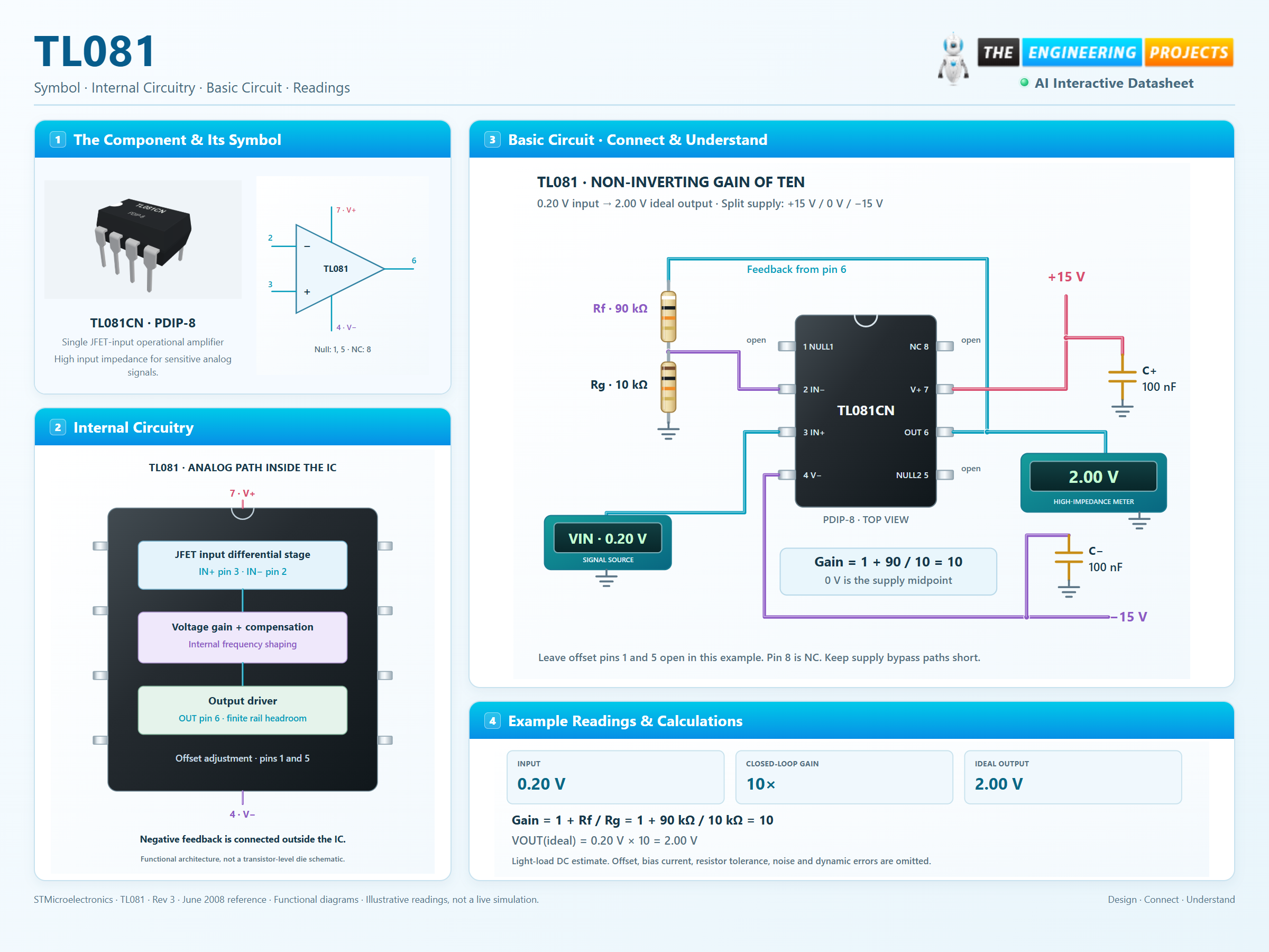
How it works
3 stages · Explore one step at a time
Sense with JFET inputs
The differential input stage has a high input impedance. Leakage still rises with temperature, so a high-impedance source needs careful board cleanliness and bias analysis.
Close the feedback loop
A 90 kΩ resistor returns the output to IN− and a 10 kΩ resistor connects that node to 0 V. Their ratio sets a nominal non-inverting gain of ten.
Allow headroom and bandwidth
The amplifier needs input and output headroom. At higher frequencies, gain-bandwidth and slew rate limit the signal independently of the resistor ratio.
Step 1 of 3
TL081 in a circuit
A physical amplifier and a clearly routed feedback network.
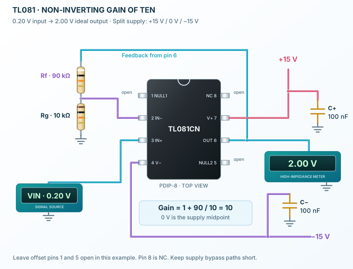
Connect it, step by step
Follow the component values and pin connections
Power both rails
Connect +15 V to pin 7 and −15 V to pin 4, with a 100 nF local bypass from each rail to ground.
Set the gain
Use 90 kΩ feedback and 10 kΩ to ground; apply VIN to IN+.
Observe the output
0.20 V becomes 2.00 V ideally. Keep the input and requested output within the specified ranges.
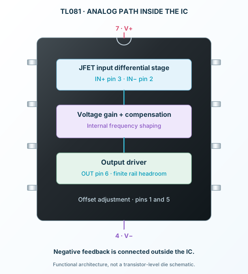
Inside TL081
A JFET input stage followed by compensated gain and an output driver.
Explore the circuit
Select a stage to see its role and connections
JFET input pair
The input pair compares IN+ and IN− with low room-temperature leakage.
Internal compensation
The gain stage includes frequency compensation for practical feedback circuits.
Output stage
The driver delivers the signal with finite rail headroom and load capability.
Selected packagePDIP-8TL081CN
Physical connections8 pinsPackage-specific numbering
Reference collection6 tables28 parameters & pin functions
Pin reference
Signal names, electrical functions and connection guidance
Physical pin numbers8 pins
Scroll within the table to see all columns and rows.
| Pin | Signal | Type | Function & connection |
|---|---|---|---|
| NULL1 | Offset null | Optional input-offset trim connection.Connection guidanceLeave open for the illustrated circuit. Use the ST offset-adjustment network if trimming is required. | |
| IN− | Inverting input | Input used by the feedback network.Connection guidanceJoin the 90 kΩ feedback resistor and 10 kΩ ground resistor. | |
| IN+ | Non-inverting input | JFET signal input.Connection guidanceApply VIN relative to the supply midpoint. Input bias current increases strongly with temperature. | |
| V− | Negative supply | Negative power rail.Connection guidanceConnect to −15 V; bypass to signal ground. | |
| NULL2 | Offset null | Second optional trim connection.Connection guidanceLeave open in the example. | |
| OUT | Analog output | Output of the internally compensated amplifier.Connection guidanceConnect the feedback resistor and a high-impedance meter. Avoid heavy or capacitive loading without checking stability and output swing. | |
| V+ | Positive supply | Positive power rail.Connection guidanceConnect to +15 V; bypass to signal ground. | |
| NC | No connection | Unused package contact.Connection guidanceLeave unconnected. |
No pins match these filters. Try another signal name or reset the filters.
Operating conditions
ST TL081C grade
Manufacturer-referenced values5 parameters
Scroll within the table to see all columns and rows.
| Parameter | Value | Conditions / notes |
|---|---|---|
| Total supply span | 6–36 V | V+ minus V− |
| Ambient temperature | 0 to +70°C | C-grade devices |
| Reference test supply | ±15 V | Used for electrical values unless stated |
| Common-mode range | ±11 V minimum; −12 to +15 V typical | ±15 V supply; see manufacturer conditions |
| Example input | 0.20 V | Relative to the 0 V midpoint |
No specifications match. Try a parameter name or a unit.
A typical range is not a guaranteed operating boundary. Use the specified minimum range for design margin.
DC characteristics
±15 V · 25°C · TL081C
Manufacturer-referenced values5 parameters
Scroll within the table to see all columns and rows.
| Parameter | Value | Conditions / notes |
|---|---|---|
| Input offset voltage | 3 mV typical; 10 mV maximum | RS = 50 Ω |
| Input resistance | 1 TΩ typical | Manufacturer Ri characteristic |
| Input offset current | 5 pA typical; 100 pA maximum | Difference between input currents at 25°C |
| No-load supply current | 1.4 mA typical; 2.5 mA maximum | Per amplifier |
| Open-loop gain | 200 V/mV typical; 25 minimum | RL = 2 kΩ; VO = ±10 V |
No specifications match. Try a parameter name or a unit.
Bias leakage rises rapidly with temperature; room-temperature leakage values do not apply over the full range.
Output and dynamic characteristics
±15 V · specified tests
Manufacturer-referenced values5 parameters
Scroll within the table to see all columns and rows.
| Parameter | Value | Conditions / notes |
|---|---|---|
| Output swing at RL = 10 kΩ | ±13.5 V typical; ±12 V minimum | 25°C |
| Output swing at RL = 2 kΩ | ±12 V typical; ±10 V minimum | 25°C |
| Gain-bandwidth product | 4 MHz typical; 2.5 MHz minimum | RL = 2 kΩ; CL = 100 pF; f = 100 kHz |
| Slew rate | 16 V/µs typical; 8 V/µs minimum | Unity gain; 10 V input step; RL = 2 kΩ; CL = 100 pF |
| Input noise density | 15 nV/√Hz typical | RS = 100 Ω; 1 kHz |
No specifications match. Try a parameter name or a unit.
Do not infer output current or stability from bandwidth alone.
Gain-of-ten example
Split-supply non-inverting stage
Manufacturer-referenced values7 parameters
Scroll within the table to see all columns and rows.
| Parameter | Value | Conditions / notes |
|---|---|---|
| Power rails | +15 V / −15 V | Pins 7 and 4 |
| Input | 0.20 V | IN+ pin 3 |
| Feedback | 90 kΩ | OUT pin 6 to IN− pin 2 |
| Ground resistor | 10 kΩ | IN− pin 2 to 0 V |
| Ideal gain / output | 10 V/V / 2.00 V | 1 + 90 / 10 |
| Bypass | 100 nF per rail | Each rail to the 0 V midpoint |
| Trim and NC | Pins 1, 5, 8 open | No offset-trim network in this circuit |
No specifications match. Try a parameter name or a unit.
The meter is high impedance. Real output includes offset, noise and resistor errors.
Package and pin reference
TL081CN · PDIP-8
Manufacturer-referenced values6 parameters
Scroll within the table to see all columns and rows.
| Parameter | Value | Conditions / notes |
|---|---|---|
| Pitch | 2.54 mm | Through-hole |
| Inputs | IN− 2; IN+ 3 | JFET differential pair |
| Output | 6 | Single analog channel |
| Power | V− 4; V+ 7 | 0 V is the external supply midpoint |
| Offset trim | 1 and 5 | Optional; consult the exact manufacturer circuit |
| No connection | 8 | Leave open |
No specifications match. Try a parameter name or a unit.
Do not confuse TL081’s single-amplifier pinout with the dual TL072 pinout.
No matching rowsTry a pin name, parameter, unit or test condition, or reset the filters.
High-impedance buffers
Buffer suitable sensor or resistor-network signals without substantial room-temperature input loading.
Manufacturer application guideActive analog filters
Combine frequency-dependent feedback with adequate gain-bandwidth and common-mode margin.
Manufacturer application guideAudio signal conditioning
Use controlled gains and AC coupling as required; verify noise, headroom and load for the complete signal chain.
Manufacturer application guideTake it into ProTech
Find TL081 in the Components Library to place its schematic symbol and connect its pins.
Reference page · circuit simulation model not yet availableOpen ProTech