Real View
A precise reference. A controlled path to ground.
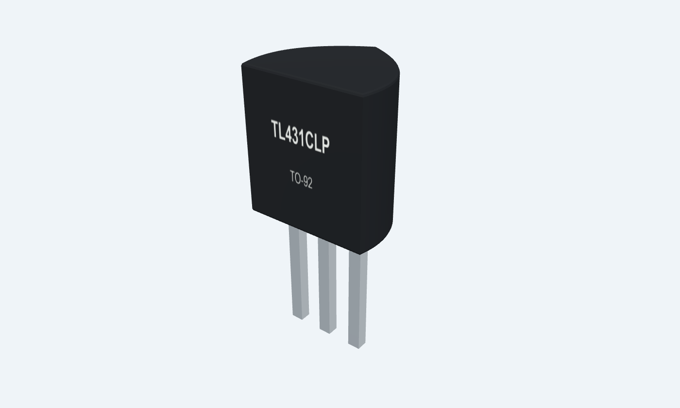
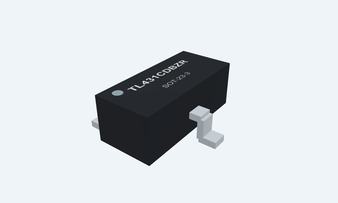
TL431 is a three-terminal adjustable shunt regulator. It compares its REF input with an internal reference and sinks current from cathode to anode to hold a resistor-selected voltage. Unlike a series regulator, it needs an external feed resistor or another controlled current source. Two feedback resistors set an output from approximately 2.495 V up to 36 V. The supply resistor must provide enough current for the load, divider and regulator at the lowest input voltage, while respecting dissipation at the highest input. This page selects TI’s standard-accuracy TL431C in TO-92 and SOT-23-3, rated from 0°C to 70°C. Their physical pin numbers differ. A and B accuracy grades, wider temperature grades and the differently pinned TL432 must be checked by their exact ordering codes.
Click a lead or use the arrow keys. Bottom view · flat edge below · 3 REF, 2 A, 1 K
The regulator sinks current from the cathode to the anode to control this voltage.
Feed through a current-limiting series resistor; connect the upper feedback resistor here.
Do not connect directly across an unrestricted supply. Recommended cathode current is 1–100 mA.
Common reference for the internal amplifier and cathode voltage.
Connect to the circuit ground and the lower divider resistor.
TO-92 physical pin 2; SOT-23 physical pin 3.
Compares the external divider node against approximately 2.495 V relative to the anode.
Connect to the junction of the two output-setting resistors.
TO-92 physical pin 3; SOT-23 physical pin 2. Reference-input current slightly raises the nominal setpoint.
Adjustable shunt regulator
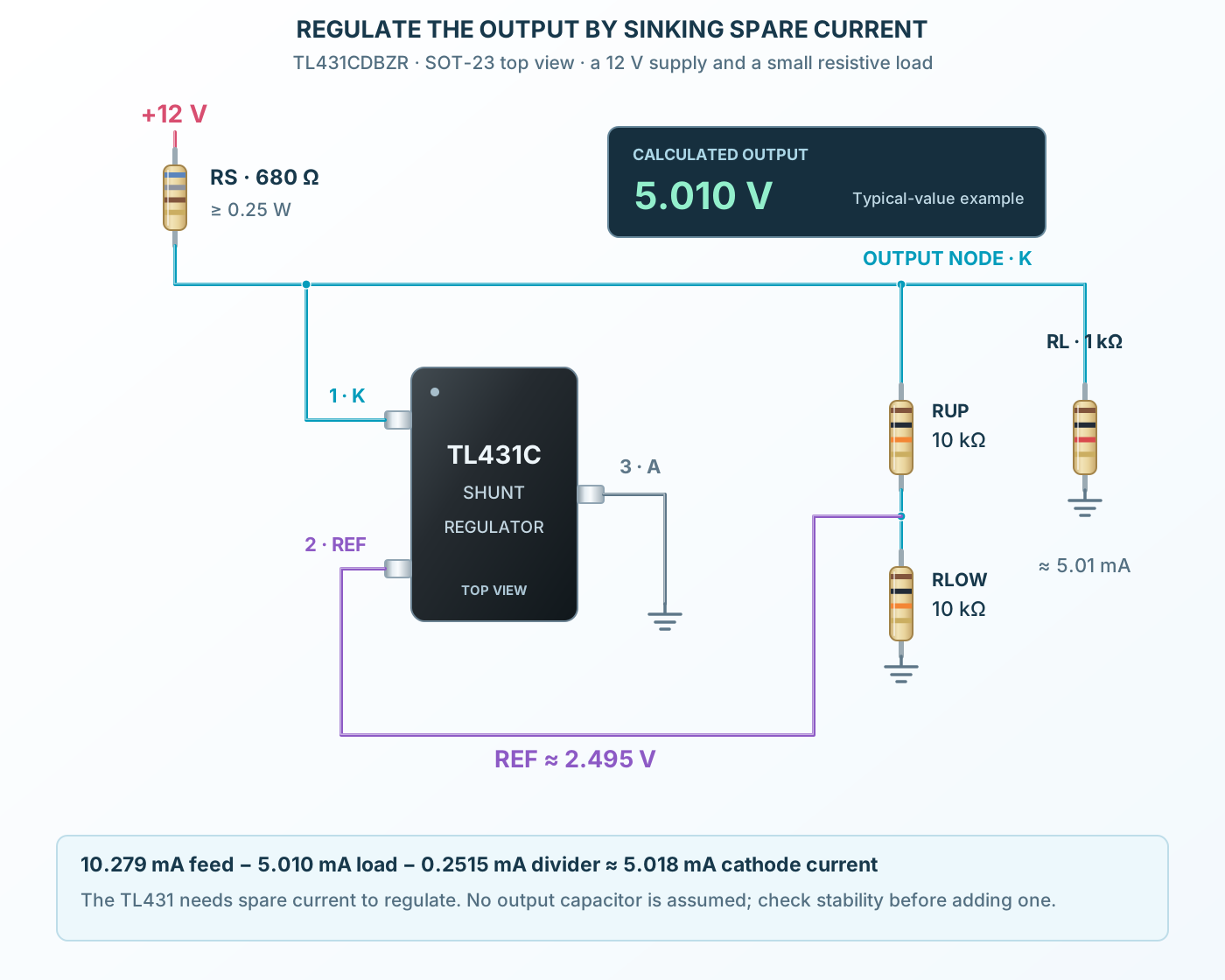
A series resistor feeds the output. The load takes its share, while the TL431 adjusts cathode current to hold the divider near its reference.
TL431CLP
Key parameters and their test conditions
Follows the selected physical package
Select a pin to open its function, electrical notes and wiring guidance.
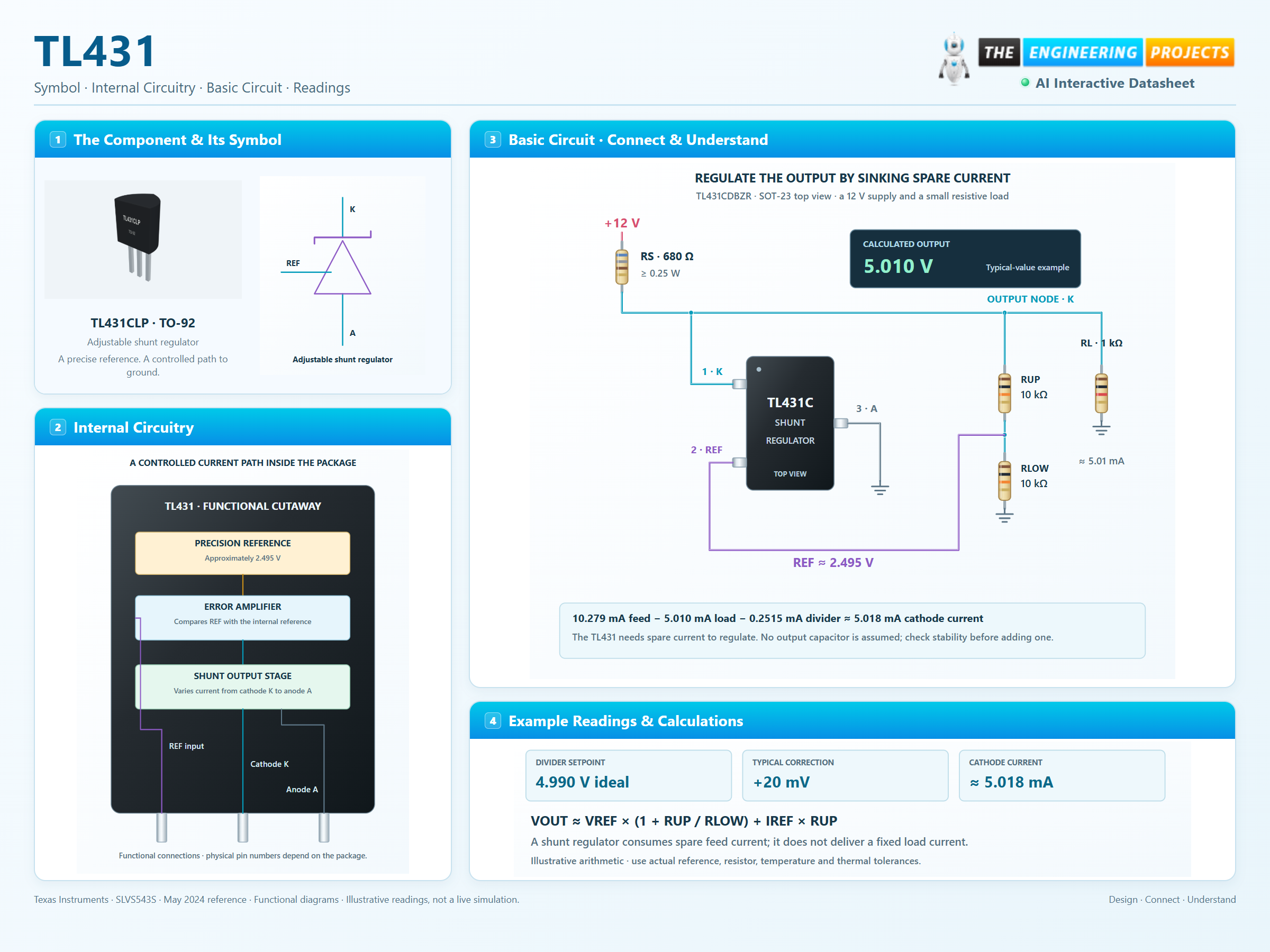
A 680 Ω resistor feeds the output from 12 V. It must cover load, divider and cathode currents.
Two 10 kΩ resistors place about 2.495 V at REF when the output is near 5 V.
The internal amplifier adjusts current from K to A. The output falls out of regulation if the load leaves too little cathode current.
For equal 10 kΩ divider resistors, 2.495 × 2 gives 4.990 V; 2 µA typical reference current adds 0.020 V. The resulting 5.01 V is illustrative, not a precision guarantee.
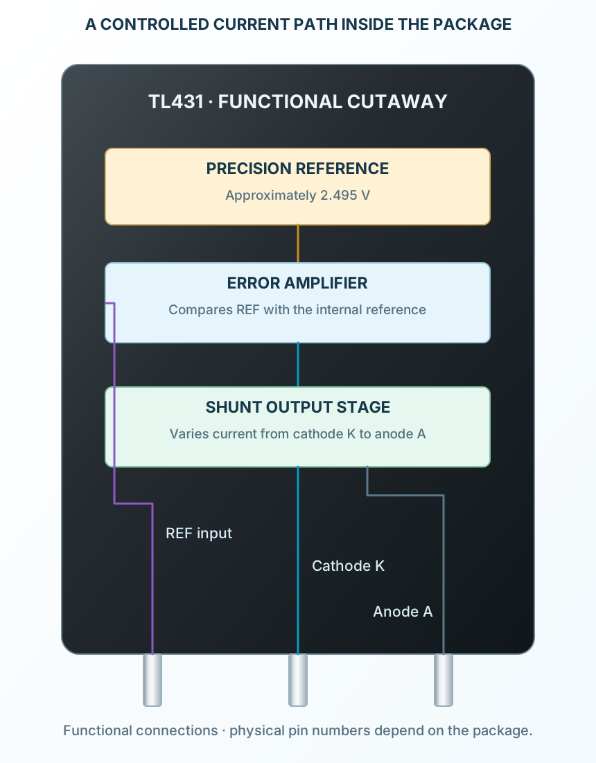
Select a pin to explore its function and connection.
| Pin | Signal | Type | Function |
|---|---|---|---|
| K | Cathode / shunt node | The regulator sinks current from the cathode to the anode to control this voltage. | |
| A | Anode / reference return | Common reference for the internal amplifier and cathode voltage. | |
| REF | Reference input | Compares the external divider node against approximately 2.495 V relative to the anode. |
No pins match. Try a signal name or choose All pins.
TI TL431C standard-accuracy grade
| Parameter | Value | Conditions / notes |
|---|---|---|
| Cathode voltage | VREF to 36 V | Referenced to the anode |
| Cathode current | 1–100 mA | Recommended range; power dissipation may impose a lower maximum |
| Ambient temperature | 0–70°C | Selected commercial C grade |
| Initial accuracy | ±2% at 25°C | A: ±1%; B: ±0.5% are different grades |
| Selected through-hole part | TL431CLP | Bulk straight-lead TO-92 |
| Selected SMD part | TL431CDBZR | SOT-23-3; different physical pin map |
No specifications match. Try a parameter name or a unit.
A shunt-current rating is not a load-current rating.
Electrical-characteristic test conditions
| Parameter | Value | Conditions / notes |
|---|---|---|
| Reference at 25°C | 2.440 / 2.495 / 2.550 V | Minimum / typical / maximum; VKA = VREF, IKA = 10 mA |
| Reference current | 2 µA typical; 4 µA maximum | IKA = 10 mA; R1 = 10 kΩ, R2 open |
| Minimum regulation current | 0.4 mA typical; 1 mA maximum | Do not design only around the typical value |
| Dynamic impedance | 0.2 Ω typical; 0.5 Ω maximum | f ≤ 1 kHz; IKA = 1–100 mA; VKA = VREF |
| Off-state cathode current | 0.1 µA typical; 1 µA maximum | VKA = 36 V; VREF input = 0 V |
| Output setting | VOUT ≈ VREF × (1 + RUP/RLOW) + IREF × RUP | Resistor tolerance and device errors remain |
No specifications match. Try a parameter name or a unit.
Initial tolerance, drift, loading and divider errors all contribute to real output accuracy.
Do not merge limits from different packages
| Parameter | Value | Conditions / notes |
|---|---|---|
| C-grade ambient | 0 to +70°C | The two orderables shown here |
| I-grade ambient | −40 to +85°C | Requires an I-grade orderable |
| Q-grade ambient | −40 to +125°C | Requires a Q-grade orderable |
| C reference change: TO-92 | 4 mV typical; 25 mV maximum | VKA = VREF; IKA = 10 mA; over C ambient range |
| C reference change: SOT-23-3 | 6 mV typical; 16 mV maximum | Different package-specific limits in the same table |
| Thermal check | TJ ≈ TA + P × θJA | Use the exact package and PCB thermal conditions |
No specifications match. Try a parameter name or a unit.
Temperature drift does not replace the initial reference-voltage tolerance.
12 V input · SOT-23-3 physical circuit
| Parameter | Value | Conditions / notes |
|---|---|---|
| Feed resistor | 680 Ω, at least 0.25 W | 12 V to K1 / output node |
| Upper divider resistor | 10 kΩ | K1 to REF2 |
| Lower divider resistor | 10 kΩ | REF2 to A3 / GND |
| Example load | 1 kΩ | Output to GND; approximately 5 mA |
| Anode | Pin 3 to GND | The TO-92 equivalent is pin 2 |
| Output capacitor | None in this teaching circuit | Capacitive-load stability must be checked before adding one |
No specifications match. Try a parameter name or a unit.
The diagram is a low-voltage teaching circuit, not a mains-connected power supply.
Illustrative typical-value arithmetic
| Parameter | Value | Conditions / notes |
|---|---|---|
| Ideal divider output | 4.990 V | 2.495 × (1 + 10/10) |
| Reference-current correction | +0.020 V | 2 µA × 10 kΩ |
| Illustrative output | 5.010 V | Before tolerances, temperature and load errors |
| Feed current | 10.279 mA | (12 − 5.01) / 680 |
| Load / upper-divider currents | 5.010 mA / 0.2515 mA | 1 kΩ load; lower-divider current plus 2 µA |
| Remaining cathode current | Approximately 5.018 mA | Feed minus load minus upper-divider current |
| Feed resistor / TL431 power | 71.9 mW / 25.1 mW | Nominal arithmetic; include worst-case input/load margins |
No specifications match. Try a parameter name or a unit.
These are calculations, not live readings or an electrical simulation.
Check orientation before connecting
| Parameter | Value | Conditions / notes |
|---|---|---|
| Cathode K | TO-92: 1 · SOT-23: 1 | Controlled shunt/output node |
| Anode A | TO-92: 2 · SOT-23: 3 | Common return |
| Reference REF | TO-92: 3 · SOT-23: 2 | Divider sense input |
| TO-92 pinout picture | Bottom view, flat edge below | Left-to-right: 3 REF, 2 A, 1 K; top-side PCB view is mirrored |
| SOT-23 pinout picture | Top view | K1 upper left, REF2 lower left, A3 at right |
| TL432 | Same function; different small-package pinouts | Do not substitute by name alone |
No specifications match. Try a parameter name or a unit.
The straight-lead TO-92 footprint is not the wider formed-lead footprint.
Stress limits are not operating targets
| Parameter | Value | Conditions / notes |
|---|---|---|
| Cathode absolute voltage | 37 V | Recommended maximum remains 36 V |
| Cathode absolute current | −100 to +150 mA | Do not use as a normal operating range |
| Reference absolute current | −0.05 to +10 mA | Input stress limit |
| Junction / storage | 150°C / −65 to +150°C | Absolute limits |
| Capacitive load | Can destabilize the shunt loop | Check the manufacturer stability curves for voltage, current and capacitance |
| Worst-case power | VKA × IKA | Evaluate high input / light load, not only the nominal circuit |
No specifications match. Try a parameter name or a unit.
Allow electrical and thermal margin, and verify stability in the actual circuit.
Set a voltage with two resistors and a suitable feed-current budget.
Manufacturer application guideControl an optocoupler LED in a properly compensated feedback circuit.
Manufacturer application guideUse the reference and cathode response for a threshold detector with suitable loading.
Manufacturer application guideFind TL431 in the Components Library to place its schematic symbol and connect its pins.
Reference page · circuit simulation model not yet availableOpen ProTech