TL494Dual-output PWM controller
One timing ramp. Controlled pulses. Two flexible outputs.
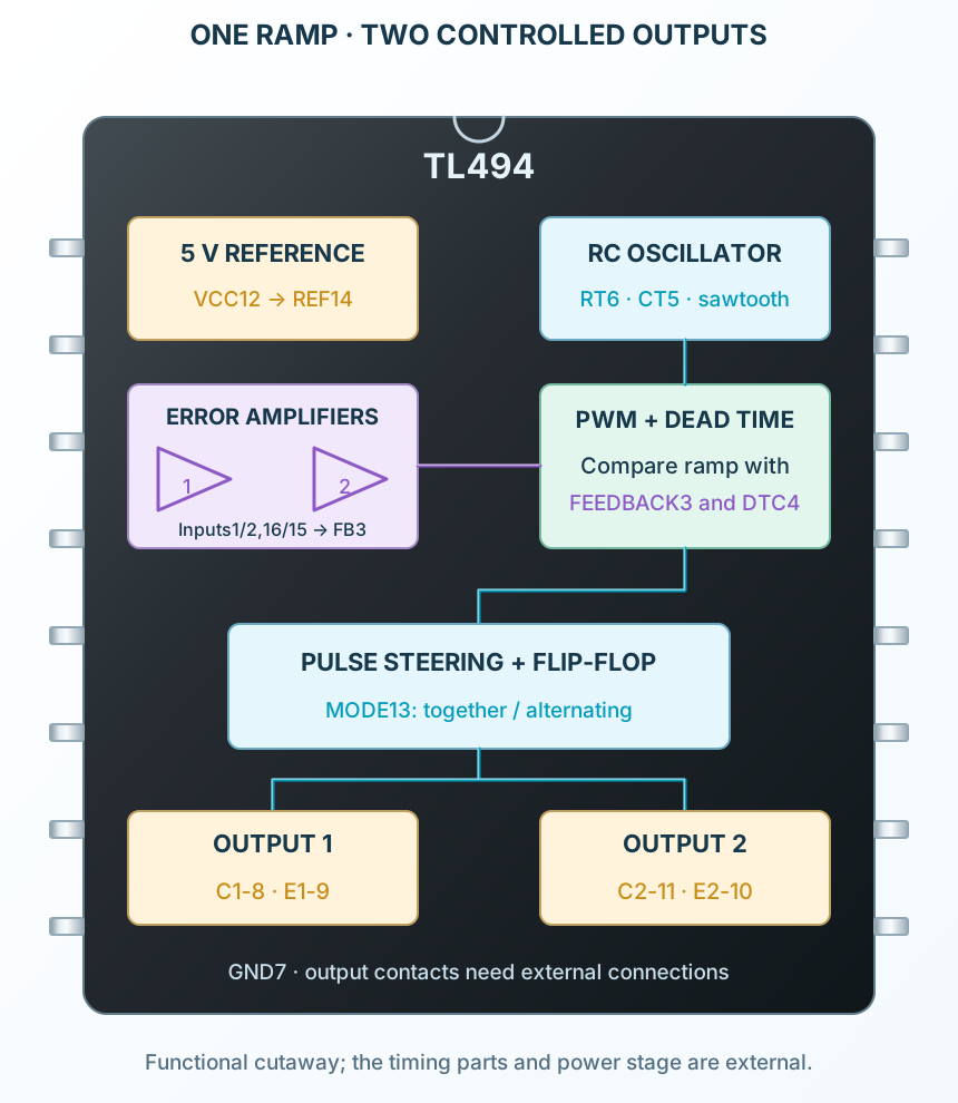
TL494 combines two error amplifiers, a timing oscillator, dead-time control, a pulse-steering circuit and two uncommitted output transistors. It generates control pulses for a power stage; it does not contain a complete regulated power converter. An external resistor and capacitor set the oscillator frequency. Feedback and dead-time voltages determine how long the outputs conduct, while pin 13 selects simultaneous or alternating output operation. The internal five-volt reference supplies small control networks. Our 12 V bench example uses only resistor-loaded outputs and a potentiometer to adjust dead time. A scope shows pulse-width changes without needing a transformer or power switch. Compare the TL494CN PDIP-16 and TL494CDR SOIC-16 package views.
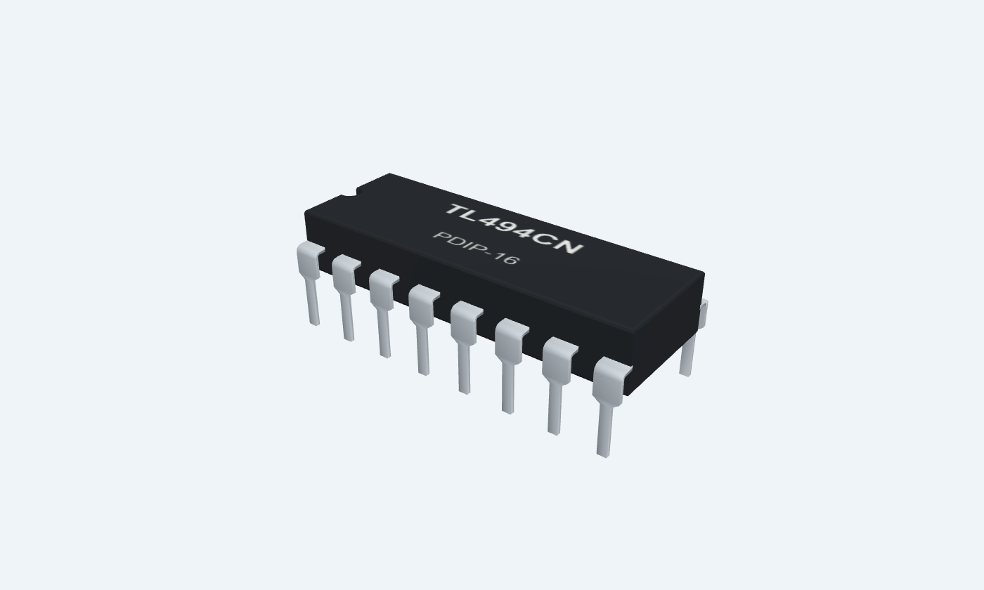
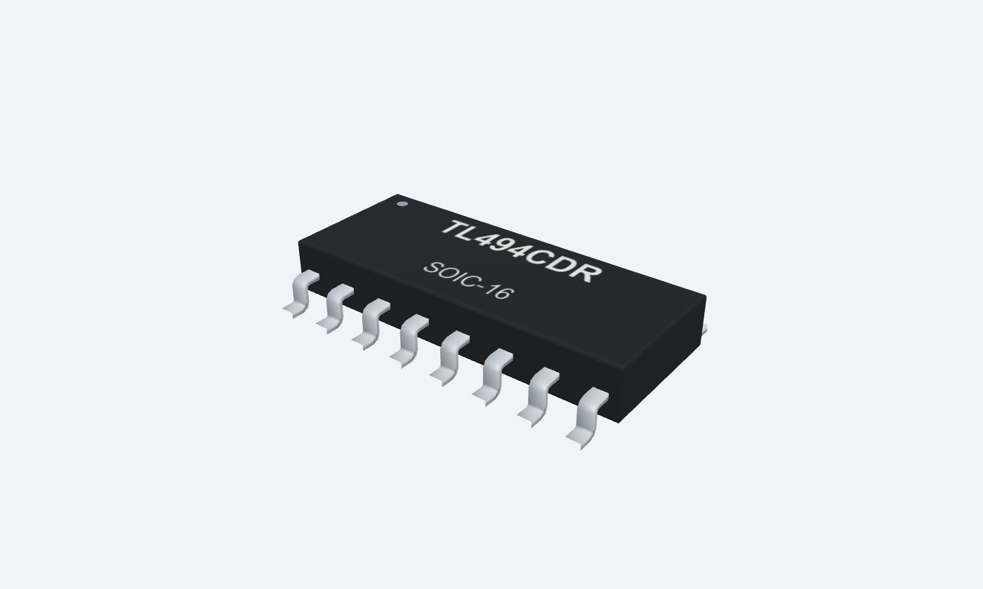

16Physical pins
TL494CNPDIP-16
Manufacturer-referencedTexas Instruments
Pin diagram
Select a pin to explore its connection
Highlight
TL494CNPDIP-16Top view
TL494CDRSOIC-16Top view
Click a lead or use the arrow keys. Top view
PIN 1 · Error amplifier inputs
Error amplifier 1 noninverting input1IN+
Function
A higher voltage than 1IN− demands shorter output pulses.
How to connect
Ground in the open-loop pulse example.
PIN 2 · Error amplifier inputs
Error amplifier 1 inverting input1IN−
Function
Reference input for the first error amplifier.
How to connect
Connect to REF14 in the open-loop example.
PIN 3 · PWM and mode control
PWM feedback nodeFEEDBACK
Function
Shared error-amplifier output and PWM control node; increasing it suppresses pulses.
How to connect
Leave externally unconnected in this DTC-controlled demonstration.
Electrical note
Do not short this node to ground while an amplifier is trying to drive it HIGH.
PIN 4 · PWM and mode control
Dead-time controlDTC
Function
Increasing this input shortens the conduction interval independently of the error amplifiers.
How to connect
Connect to the wiper of a 10 kΩ potentiometer between REF14 and GND.
Electrical note
Start with the wiper near REF for outputs OFF, then reduce it slowly.
PIN 5 · Oscillator network
Oscillator capacitorCT
Function
Charges and discharges to form the internal timing ramp.
How to connect
Connect 1 nF to GND; keep the loop short.
PIN 6 · Oscillator network
Oscillator resistorRT
Function
Sets the timing capacitor charging current.
How to connect
Connect 100 kΩ to GND.
PIN 7 · Ground
Common returnGND
Function
Reference for control, oscillator and supply.
How to connect
Join bypass, timing and scope returns.
PIN 8 · Uncommitted outputs
Output transistor 1 upper contactC1
Function
Uncommitted output contact; the example uses it as a pulled-up switching output.
How to connect
Connect 4.7 kΩ to +12 V and a high-impedance scope channel.
Electrical note
Output goes LOW when its transistor conducts.
PIN 9 · Uncommitted outputs
Output transistor 1 lower contactE1
Function
Return-side contact of output transistor 1.
How to connect
Ground in this sinking-output example.
PIN 10 · Uncommitted outputs
Output transistor 2 lower contactE2
Function
Return-side contact of output transistor 2.
How to connect
Ground in this sinking-output example.
PIN 11 · Uncommitted outputs
Output transistor 2 upper contactC2
Function
Second uncommitted output contact.
How to connect
Connect its own 4.7 kΩ to +12 V and the second scope channel.
PIN 12 · Supply
Control supplyVCC
Function
Supplies the controller and reference regulator.
How to connect
Apply +12 V with 100 nF and local bulk decoupling to GND.
PIN 13 · PWM and mode control
Output mode selectionOUTPUT CTRL
Function
LOW selects simultaneous single-ended operation; REF selects alternating push-pull operation.
How to connect
Tie to GND in the main example. Change modes only with power removed.
Electrical note
This mode pin is not intended as a PWM switching input.
PIN 14 · Bias reference
Five-volt reference outputREF
Function
Regulated reference for bias and control networks.
How to connect
Bypass with 100 nF; connect the control potentiometer and amplifier inverting inputs.
Electrical note
Reference current is limited; it does not supply motors or power loads.
PIN 15 · Error amplifier inputs
Error amplifier 2 inverting input2IN−
Function
Reference input for the second amplifier.
How to connect
Connect to REF14 in the open-loop example.
PIN 16 · Error amplifier inputs
Error amplifier 2 noninverting input2IN+
Function
A higher voltage than 2IN− demands shorter pulses.
How to connect
Ground in the open-loop example.
Key specifications
The error amplifiers and dead-time input can each reduce the output conduction interval. Output mode determines whether the two channels pulse together or alternate.
Recommended VCC7–40 V
Reference output5 V nominal · ±5% initial
Oscillator range1–300 kHz
Selected C grade0–70 °C
Package details
TL494CN · PDIP-16
| Property | Details |
|---|---|
| Manufacturer | Texas Instruments |
| Part number | TL494CN |
| Package | PDIP-16 |
| Connections | 16 pins |
| Mounting | Through-hole |
| Lead pitch | 2.54 mm |
| Package code | PDIP-16 |
| Thermal reference | See operating and package limits |
Operating conditions
TL494C selected variants
Manufacturer specifications 7 parameters
Scroll sideways to see all columns.
| Parameter | Value | Conditions / notes |
|---|---|---|
| Control supply | 7–40 V | 12 V bench circuit |
| Ambient temperature | 0 to +70°C | C grade; I grade is a different ordering choice |
| Oscillator frequency | 1–300 kHz | Recommended range |
| Timing resistor | 1.8–500 kΩ | RT to ground |
| Timing capacitor | 0.47–10000 nF | CT to ground |
| Amplifier input common mode | −0.3 V to VCC−2 V | Do not exceed the valid range |
| Output current | Up to 200 mA per transistor | Check voltage drop, thermal conditions and external limits |
No specifications match. Try a parameter name or a unit.
Output current capability does not mean the IC includes a safe power-stage current limiter.
Reference and feedback
Specified test conditions
Manufacturer specifications 6 parameters
Scroll sideways to see all columns.
| Parameter | Value | Conditions / notes |
|---|---|---|
| REF at 1 mA | 4.75–5.25 V; 5 V typical | Specified supply and temperature conditions |
| Reference external load | Up to 10 mA available for bias | Includes the potentiometer and other external loads |
| Feedback input sink | 0.3 mA minimum, 0.7 mA typical | FEEDBACK = 0.7 V |
| PWM zero-duty threshold | 3.4 V typical, 4.5 V maximum | Feedback control test |
| Error amplifier offset | 2 mV typical, 10 mV maximum | Specified electrical test |
| Error amplifier gain | 80 dB typical, 70 dB minimum | Specified load and output range |
No specifications match. Try a parameter name or a unit.
The reference is for control bias; it is not a general-purpose supply rail.
Output modes
Configure OUTPUT CTRL as a fixed logic level
Manufacturer specifications 6 parameters
Scroll sideways to see all columns.
| Parameter | Value | Conditions / notes |
|---|---|---|
| Pin 13 to GND | Single-ended / simultaneous | Both outputs can conduct during the same oscillator cycle |
| Pin 13 to REF | Push-pull / alternating | Each output receives every other oscillator cycle |
| Single-ended frequency | fOUT ≈ fOSC | Same period per channel |
| Push-pull frequency | fOUT ≈ fOSC / 2 | Twice the period per channel |
| Grounded DTC | Maximum allowed conduction | Internal blanking still prevents an ideal 100% duty |
| Increasing DTC | Shorter conduction pulses | Around 3.3 V can command zero duty under specified conditions |
No specifications match. Try a parameter name or a unit.
At the pulled-up C outputs used here, transistor conduction appears as a LOW pulse.
Resistor-loaded pulse circuit
No external power stage
Manufacturer specifications 9 parameters
Scroll sideways to see all columns.
| Parameter | Value | Conditions / notes |
|---|---|---|
| VCC12 / GND7 | +12 V / common GND | 100 nF and local bulk bypass |
| REF14 | 100 nF to GND | Feeds both inverting amplifier inputs and 10 kΩ pot |
| Amplifier inputs | 1 / 16 to GND; 2 / 15 to REF | Keeps the error amplifiers from demanding shutdown |
| FEEDBACK3 | No external connection | Internal amplifier/bias network still determines its voltage |
| DTC4 | Potentiometer wiper | Pot ends REF and GND; start HIGH |
| CT5 / RT6 | 1 nF / 100 kΩ to GND | Nominal 10 kHz design equation |
| Mode13 | GND | Simultaneous operation |
| Outputs | E1-9 / E2-10 to GND | C1-8 and C2-11 each pull up to +12 V through 4.7 kΩ |
| Measurement | High-impedance two-channel scope | Observe each C output relative to GND |
No specifications match. Try a parameter name or a unit.
Do not attach a motor or transformer to this demonstration; output loads are deliberately small.
Frequency and example calculations
First-order design values
Manufacturer specifications 7 parameters
Scroll sideways to see all columns.
| Parameter | Value | Conditions / notes |
|---|---|---|
| Oscillator | 1/(100000 Ω × 1 nF) = 10 kHz | Nominal approximation |
| Oscillator period | 100 µs | Inverse of 10 kHz |
| Single-ended output period | 100 µs | Same as oscillator |
| Push-pull per-output period | 200 µs | 5 kHz on each output |
| Approximate pulled-up load | 12 V / 4.7 kΩ = 2.55 mA | Ignoring switch voltage drop |
| Worst resistor power at continuous ON | 12² / 4700 ≈ 31 mW | Use suitable voltage and power ratings |
| Potentiometer reference load | 5 V / 10 kΩ = 0.5 mA | Plus other reference loads |
No specifications match. Try a parameter name or a unit.
Real timing varies with component tolerances and oscillator characteristics.
Layout and integration
Keep control wiring distinct from a power stage
Manufacturer specifications 6 parameters
Scroll sideways to see all columns.
| Parameter | Value | Conditions / notes |
|---|---|---|
| Timing loop | Short CT/RT ground return | Keep away from switching nodes |
| Reference bypass | Close to REF14 and GND7 | Avoid loading the reference excessively |
| Supply bypass | Close to VCC12 and GND7 | Add suitable local bulk capacitance |
| Feedback compensation | Application-specific | Needed for stable closed-loop regulation |
| Output polarity | LOW at C when sinking | An external follower connection has a different waveform |
| Power switch drive | Separate design task | Check gate charge, edge speed and protection |
No specifications match. Try a parameter name or a unit.
A clear bench waveform alone does not validate a complete switching converter.
Package and stress limits
TL494CN · PDIP-16
Manufacturer specifications 6 parameters
Scroll sideways to see all columns.
| Parameter | Value | Conditions / notes |
|---|---|---|
| PDIP | TL494CN · N package | 16 pins, 2.54 mm pitch |
| SOIC | TL494CDR · D package | 16 pins, 1.27 mm pitch |
| Supply stress | 41 V absolute maximum | Normal operation maximum is 40 V |
| Output current stress | 250 mA absolute maximum | Recommended current maximum is 200 mA with conditions |
| Storage | −65 to +150°C | Unpowered |
| Outputs C/E | Keep the manufacturer pin names | The current revision describes the switching output implementation separately from legacy terminology |
No specifications match. Try a parameter name or a unit.
Use the selected orderable and datasheet revision rather than mixing limits from different manufacturers.
Connections by function
Select a pin for its function, connection guidance and electrical notes.
Error amplifier inputs4 pins
PWM and mode control3 pins
Oscillator network2 pins
Ground1 pin
Uncommitted outputs4 pins
Supply1 pin
Bias reference1 pin
Error amplifier inputs4 pins
PWM and mode control3 pins
Oscillator network2 pins
Ground1 pin
Uncommitted outputs4 pins
Supply1 pin
Bias reference1 pin
TL494 at a glance
Follow the labeled connections and functional stages
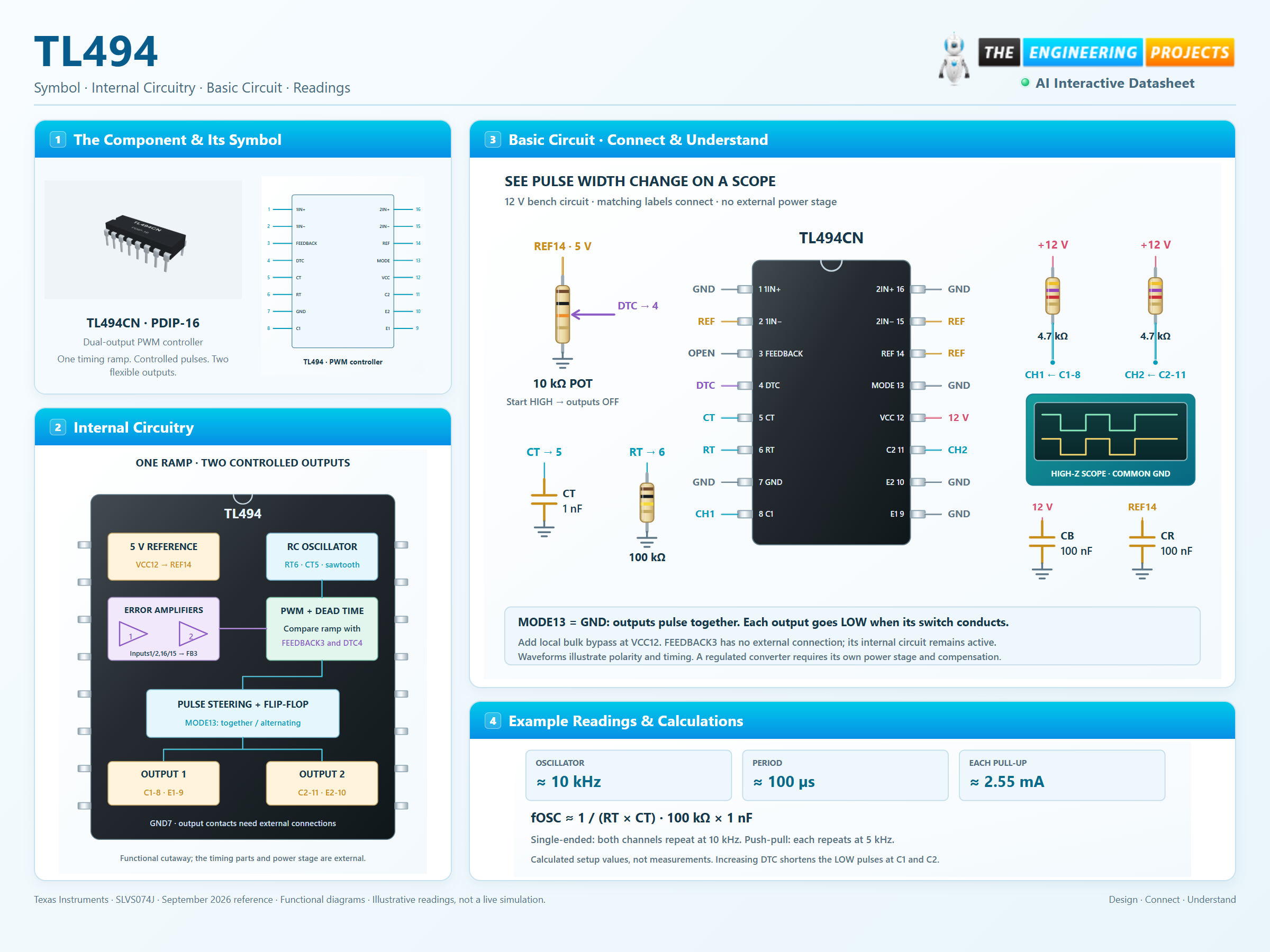
How it works
3 stages · Explore one step at a time
Generate a timing ramp
RT6 and CT5 establish the sawtooth period. The first-order design equation is fOSC ≈ 1/(RT × CT).
Limit pulse duration
The PWM and dead-time comparators suppress conduction when their control voltage exceeds the active timing ramp.
Steer the outputs
Pin 13 chooses simultaneous pulses or alternating channels. Each C/E pair needs a suitable external connection and load.
Step 1 of 3
TL494 in a circuit
A 12 V controller with low-current resistive loads.
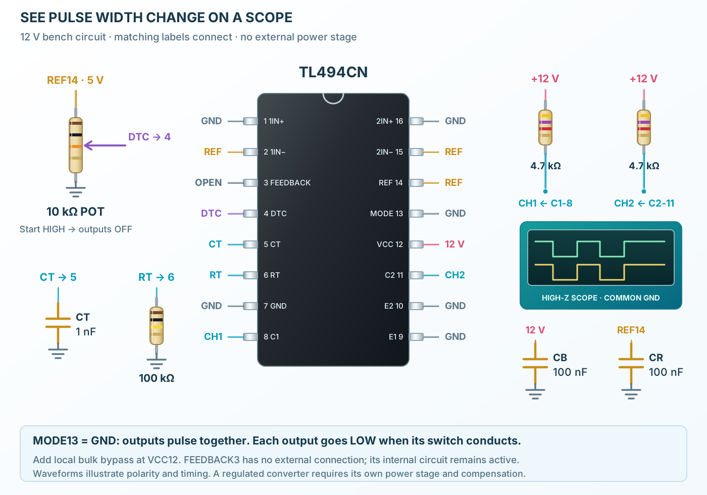
Connect it, step by step
Follow the component values and pin connections
Set a nominal 10 kHz clock
Connect 1 nF to CT and 100 kΩ to RT, both returning to ground.
Adjust dead time
Turn the REF-powered potentiometer from HIGH toward LOW and observe the growing LOW pulses at C1/C2.
Compare modes
Power down before changing pin 13 from GND to REF. Push-pull mode alternates the channels and halves each output frequency.
Inside TL494
Timing, pulse control and output steering inside one controller.
Explore the circuit
Select a stage to see its role and connections
Create a stable ramp
The reference and RC oscillator establish the timing waveform.
Compare control demands
Either error amplifier or DTC can reduce pulse duration.
Select the output pattern
The mode pin selects simultaneous or alternating output switching.
Selected packagePDIP-16TL494CN
Physical connections16 pinsPackage-specific numbering
Reference collection8 tables47 parameters & pin functions
Pin reference
Signal names, electrical functions and connection guidance
Physical pin numbers16 pins
Scroll within the table to see all columns and rows.
| Pin | Signal | Type | Function & connection |
|---|---|---|---|
| 1IN+ | Error amplifier 1 noninverting input | A higher voltage than 1IN− demands shorter output pulses.Connection guidanceGround in the open-loop pulse example. | |
| 1IN− | Error amplifier 1 inverting input | Reference input for the first error amplifier.Connection guidanceConnect to REF14 in the open-loop example. | |
| FEEDBACK | PWM feedback node | Shared error-amplifier output and PWM control node; increasing it suppresses pulses.Connection guidanceLeave externally unconnected in this DTC-controlled demonstration. Do not short this node to ground while an amplifier is trying to drive it HIGH. | |
| DTC | Dead-time control | Increasing this input shortens the conduction interval independently of the error amplifiers.Connection guidanceConnect to the wiper of a 10 kΩ potentiometer between REF14 and GND. Start with the wiper near REF for outputs OFF, then reduce it slowly. | |
| CT | Oscillator capacitor | Charges and discharges to form the internal timing ramp.Connection guidanceConnect 1 nF to GND; keep the loop short. | |
| RT | Oscillator resistor | Sets the timing capacitor charging current.Connection guidanceConnect 100 kΩ to GND. | |
| GND | Common return | Reference for control, oscillator and supply.Connection guidanceJoin bypass, timing and scope returns. | |
| C1 | Output transistor 1 upper contact | Uncommitted output contact; the example uses it as a pulled-up switching output.Connection guidanceConnect 4.7 kΩ to +12 V and a high-impedance scope channel. Output goes LOW when its transistor conducts. | |
| E1 | Output transistor 1 lower contact | Return-side contact of output transistor 1.Connection guidanceGround in this sinking-output example. | |
| E2 | Output transistor 2 lower contact | Return-side contact of output transistor 2.Connection guidanceGround in this sinking-output example. | |
| C2 | Output transistor 2 upper contact | Second uncommitted output contact.Connection guidanceConnect its own 4.7 kΩ to +12 V and the second scope channel. | |
| VCC | Control supply | Supplies the controller and reference regulator.Connection guidanceApply +12 V with 100 nF and local bulk decoupling to GND. | |
| OUTPUT CTRL | Output mode selection | LOW selects simultaneous single-ended operation; REF selects alternating push-pull operation.Connection guidanceTie to GND in the main example. Change modes only with power removed. This mode pin is not intended as a PWM switching input. | |
| REF | Five-volt reference output | Regulated reference for bias and control networks.Connection guidanceBypass with 100 nF; connect the control potentiometer and amplifier inverting inputs. Reference current is limited; it does not supply motors or power loads. | |
| 2IN− | Error amplifier 2 inverting input | Reference input for the second amplifier.Connection guidanceConnect to REF14 in the open-loop example. | |
| 2IN+ | Error amplifier 2 noninverting input | A higher voltage than 2IN− demands shorter pulses.Connection guidanceGround in the open-loop example. |
No pins match these filters. Try another signal name or reset the filters.
Operating conditions
TL494C selected variants
Manufacturer-referenced values7 parameters
Scroll within the table to see all columns and rows.
| Parameter | Value | Conditions / notes |
|---|---|---|
| Control supply | 7–40 V | 12 V bench circuit |
| Ambient temperature | 0 to +70°C | C grade; I grade is a different ordering choice |
| Oscillator frequency | 1–300 kHz | Recommended range |
| Timing resistor | 1.8–500 kΩ | RT to ground |
| Timing capacitor | 0.47–10000 nF | CT to ground |
| Amplifier input common mode | −0.3 V to VCC−2 V | Do not exceed the valid range |
| Output current | Up to 200 mA per transistor | Check voltage drop, thermal conditions and external limits |
No specifications match. Try a parameter name or a unit.
Output current capability does not mean the IC includes a safe power-stage current limiter.
Reference and feedback
Specified test conditions
Manufacturer-referenced values6 parameters
Scroll within the table to see all columns and rows.
| Parameter | Value | Conditions / notes |
|---|---|---|
| REF at 1 mA | 4.75–5.25 V; 5 V typical | Specified supply and temperature conditions |
| Reference external load | Up to 10 mA available for bias | Includes the potentiometer and other external loads |
| Feedback input sink | 0.3 mA minimum, 0.7 mA typical | FEEDBACK = 0.7 V |
| PWM zero-duty threshold | 3.4 V typical, 4.5 V maximum | Feedback control test |
| Error amplifier offset | 2 mV typical, 10 mV maximum | Specified electrical test |
| Error amplifier gain | 80 dB typical, 70 dB minimum | Specified load and output range |
No specifications match. Try a parameter name or a unit.
The reference is for control bias; it is not a general-purpose supply rail.
Output modes
Configure OUTPUT CTRL as a fixed logic level
Manufacturer-referenced values6 parameters
Scroll within the table to see all columns and rows.
| Parameter | Value | Conditions / notes |
|---|---|---|
| Pin 13 to GND | Single-ended / simultaneous | Both outputs can conduct during the same oscillator cycle |
| Pin 13 to REF | Push-pull / alternating | Each output receives every other oscillator cycle |
| Single-ended frequency | fOUT ≈ fOSC | Same period per channel |
| Push-pull frequency | fOUT ≈ fOSC / 2 | Twice the period per channel |
| Grounded DTC | Maximum allowed conduction | Internal blanking still prevents an ideal 100% duty |
| Increasing DTC | Shorter conduction pulses | Around 3.3 V can command zero duty under specified conditions |
No specifications match. Try a parameter name or a unit.
At the pulled-up C outputs used here, transistor conduction appears as a LOW pulse.
Resistor-loaded pulse circuit
No external power stage
Manufacturer-referenced values9 parameters
Scroll within the table to see all columns and rows.
| Parameter | Value | Conditions / notes |
|---|---|---|
| VCC12 / GND7 | +12 V / common GND | 100 nF and local bulk bypass |
| REF14 | 100 nF to GND | Feeds both inverting amplifier inputs and 10 kΩ pot |
| Amplifier inputs | 1 / 16 to GND; 2 / 15 to REF | Keeps the error amplifiers from demanding shutdown |
| FEEDBACK3 | No external connection | Internal amplifier/bias network still determines its voltage |
| DTC4 | Potentiometer wiper | Pot ends REF and GND; start HIGH |
| CT5 / RT6 | 1 nF / 100 kΩ to GND | Nominal 10 kHz design equation |
| Mode13 | GND | Simultaneous operation |
| Outputs | E1-9 / E2-10 to GND | C1-8 and C2-11 each pull up to +12 V through 4.7 kΩ |
| Measurement | High-impedance two-channel scope | Observe each C output relative to GND |
No specifications match. Try a parameter name or a unit.
Do not attach a motor or transformer to this demonstration; output loads are deliberately small.
Frequency and example calculations
First-order design values
Manufacturer-referenced values7 parameters
Scroll within the table to see all columns and rows.
| Parameter | Value | Conditions / notes |
|---|---|---|
| Oscillator | 1/(100000 Ω × 1 nF) = 10 kHz | Nominal approximation |
| Oscillator period | 100 µs | Inverse of 10 kHz |
| Single-ended output period | 100 µs | Same as oscillator |
| Push-pull per-output period | 200 µs | 5 kHz on each output |
| Approximate pulled-up load | 12 V / 4.7 kΩ = 2.55 mA | Ignoring switch voltage drop |
| Worst resistor power at continuous ON | 12² / 4700 ≈ 31 mW | Use suitable voltage and power ratings |
| Potentiometer reference load | 5 V / 10 kΩ = 0.5 mA | Plus other reference loads |
No specifications match. Try a parameter name or a unit.
Real timing varies with component tolerances and oscillator characteristics.
Layout and integration
Keep control wiring distinct from a power stage
Manufacturer-referenced values6 parameters
Scroll within the table to see all columns and rows.
| Parameter | Value | Conditions / notes |
|---|---|---|
| Timing loop | Short CT/RT ground return | Keep away from switching nodes |
| Reference bypass | Close to REF14 and GND7 | Avoid loading the reference excessively |
| Supply bypass | Close to VCC12 and GND7 | Add suitable local bulk capacitance |
| Feedback compensation | Application-specific | Needed for stable closed-loop regulation |
| Output polarity | LOW at C when sinking | An external follower connection has a different waveform |
| Power switch drive | Separate design task | Check gate charge, edge speed and protection |
No specifications match. Try a parameter name or a unit.
A clear bench waveform alone does not validate a complete switching converter.
Package and stress limits
TL494CN · PDIP-16
Manufacturer-referenced values6 parameters
Scroll within the table to see all columns and rows.
| Parameter | Value | Conditions / notes |
|---|---|---|
| PDIP | TL494CN · N package | 16 pins, 2.54 mm pitch |
| SOIC | TL494CDR · D package | 16 pins, 1.27 mm pitch |
| Supply stress | 41 V absolute maximum | Normal operation maximum is 40 V |
| Output current stress | 250 mA absolute maximum | Recommended current maximum is 200 mA with conditions |
| Storage | −65 to +150°C | Unpowered |
| Outputs C/E | Keep the manufacturer pin names | The current revision describes the switching output implementation separately from legacy terminology |
No specifications match. Try a parameter name or a unit.
Use the selected orderable and datasheet revision rather than mixing limits from different manufacturers.
No matching rowsTry a pin name, parameter, unit or test condition, or reset the filters.
Switching supply control
Drive a separately engineered switching converter with compensation and protection.
Manufacturer application guidePush-pull timing
Generate alternating control pulses with a defined off interval.
Manufacturer application guidePWM teaching
Observe how timing, feedback and dead time affect resistor-loaded waveforms.
Manufacturer application guideTake it into ProTech
Find TL494 in the Components Library to place its schematic symbol and connect its pins.
Reference page · circuit simulation model not yet availableOpen ProTech