TLV1117-33800 mA fixed-output linear regulator
A compact 3.3 V supply, with silicon revision made explicit.
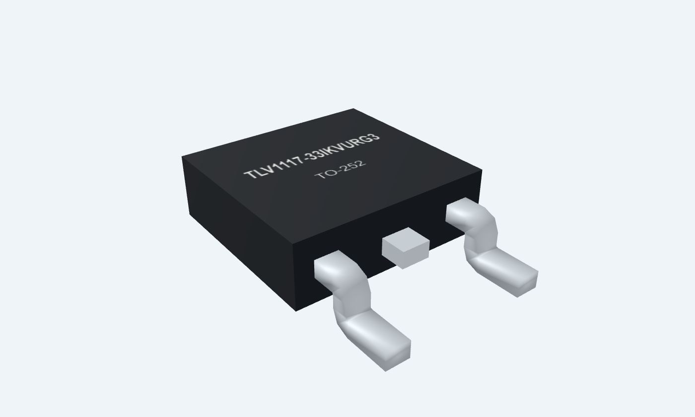
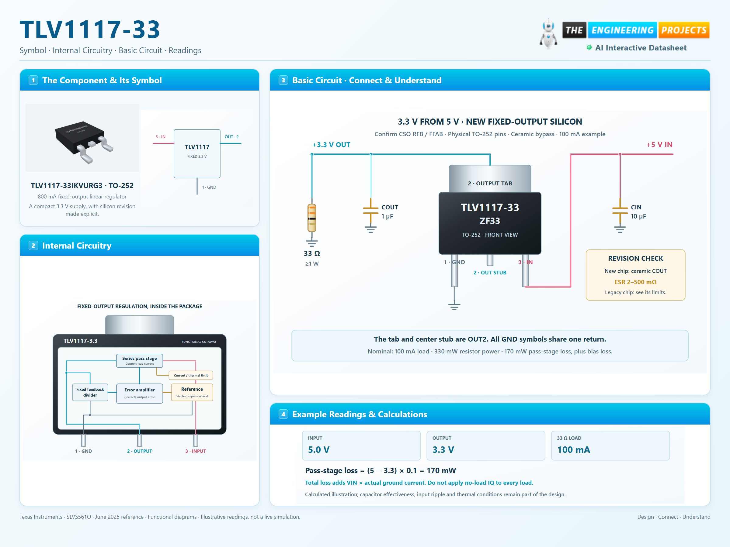
TLV1117-33 is a fixed 3.3 V linear regulator with an 800 mA output-current class. It converts a higher DC supply into a regulated rail through a series-pass stage. Its available current depends on dropout headroom, board cooling and the 125°C operating junction limit. The selected TLV1117-33IKVURG3 uses a TO-252 surface-mount package: GND1, OUT2 and IN3, with the exposed tab connected to OUT. The Real View, interactive pinout, 3D model and downloadable footprint all describe this exact package. TI specifies both legacy and newer silicon under this family. Their dropout, bias current and capacitor requirements differ. Check the shipment’s CSO identifier before applying the new-chip ceramic-capacitor example: SFB identifies legacy silicon; RFB or FFAB identifies new silicon.

3Physical pins
TLV1117-33IKVURG3TO-252
Manufacturer-referencedTexas Instruments
Pin diagram
Select a pin to explore its connection
Highlight
TLV1117-33TO-252Front face · leads down · 1 GND, 2 OUT, 3 IN; tab OUT
Click a lead or use the arrow keys. Front face · leads down · 1 GND, 2 OUT, 3 IN; tab OUT
PIN 1 · Ground
Ground referenceGND
Function
Reference and bias return for the fixed 3.3 V regulator.
How to connect
Join input return, capacitor returns and load ground locally.
Electrical note
Lead 1. The tab is OUTPUT, not ground.
PIN 2 · Regulated output and tab
Regulated output and tabOUT
Function
Fixed 3.3 V output; also connected to the large exposed tab.
How to connect
Connect the load and output stability capacitor here.
Electrical note
Lead 2 and exposed thermal tab are one electrical node.
PIN 3 · Supply
Supply inputIN
Function
Input to the protected series-pass stage.
How to connect
Use +5 V with local ceramic bypass in the illustrated circuit.
Electrical note
Recommended 4.7–15 V for this output; allow dropout and ripple margin.
Key specifications
The voltage name is shared, but legacy and new fixed-output silicon have different dropout, ground current and stability requirements.
Fixed output3.3 V nominal
Current class800 mA · thermally limited
New-chip no-load bias65 µA typical at 15 V
I-grade junction range−40–125 °C recommended
Package details
TLV1117-33IKVURG3 · TO-252
| Property | Details |
|---|---|
| Manufacturer | Texas Instruments |
| Part number | TLV1117-33IKVURG3 |
| Package | TO-252 |
| Connections | 3 pins |
| Mounting | SMD |
| Lead pitch | 2.29 mm |
| Package code | KVU |
| Thermal reference | New-chip θJA 67.2°C/W under TI board conditions; actual mounting changes temperature rise |
Exact order and silicon revision
One verified fixed-3.3 V package
Manufacturer specifications 6 parameters
Scroll sideways to see all columns.
| Parameter | Value | Conditions / notes |
|---|---|---|
| Selected order | TLV1117-33IKVURG3 | TO-252 KVU; industrial junction range |
| Package marking | ZF33 | Manufacturer marking plus traceability data |
| Physical electrical nodes | 1 GND; 2 OUT/tab; 3 IN | Metal tab must not be grounded |
| Legacy chip identifier | CSO SFB | Use legacy limits and stability guidance |
| New chip identifiers | CSO RFB or FFAB | Use new fixed-output specifications |
| Through-hole option | Not offered on this page | No matching fixed-3.3 V through-hole order verified in the selected order table |
No specifications match. Try a parameter name or a unit.
Package illustrations show identity; use the shipment label to distinguish silicon.
Operating range and accuracy
Selected I-grade device
Manufacturer specifications 8 parameters
Scroll sideways to see all columns.
| Parameter | Value | Conditions / notes |
|---|---|---|
| Recommended input | 4.7–15 V | Add ripple margin above worst-case dropout |
| Absolute maximum input | 16 V | Stress rating only |
| Output current | 0–800 mA | Limited by heat and source headroom |
| Recommended junction | −40 to 125°C | Not the ambient-temperature rating |
| Output at 25°C | 3.267–3.333 V | VIN5 V, 10 mA load |
| I-grade output over specified range | 3.168–3.432 V | VIN4.75–10 V; 0–800 mA; full temperature |
| I-grade line regulation | 1 mV typical; 10 mV maximum | VIN4.75–15 V, no load |
| I-grade load regulation | 1 mV typical; 15 mV maximum | VIN4.75 V; 0–800 mA |
No specifications match. Try a parameter name or a unit.
C-grade temperature and accuracy limits are not substituted.
Dropout: legacy versus new
I-grade limits; load matters
Manufacturer specifications 6 parameters
Scroll sideways to see all columns.
| Parameter | Value | Conditions / notes |
|---|---|---|
| Legacy at 100 mA | 1.1 V typical; 1.3 V maximum | Output dropout test |
| Legacy at 500 mA | 1.15 V typical; 1.35 V maximum | Output dropout test |
| Legacy at 800 mA | 1.2 V typical; 1.4 V maximum | Output dropout test |
| New fixed chip at 100 mA | 0.2 V typical; 0.4 V maximum | New-chip specification |
| New fixed chip at 500 mA | 0.5 V typical; 0.8 V maximum | New-chip specification |
| New fixed chip at 800 mA | 0.8 V typical; 1.2 V maximum | New-chip specification |
No specifications match. Try a parameter name or a unit.
The family operating input range still applies; dropout alone does not define the minimum permitted input.
Ground current and protection
Do not mix the silicon columns
Manufacturer specifications 6 parameters
Scroll sideways to see all columns.
| Parameter | Value | Conditions / notes |
|---|---|---|
| Legacy fixed-output ground current | 5 mA typical; 15 mA maximum | VIN≤15 V |
| New fixed no-load ground current | 65 µA typical; 110 µA maximum | VIN15 V; not a full-load bias specification |
| Legacy current limit | 0.8 A min.; 1.2 A typ.; 1.6 A max. | 5 V input/output differential, 25°C |
| New fixed current limit | 1.1 A typical; 1.6 A maximum | VOUT=90% nominal; specified input headroom |
| New fixed short-circuit current | 150–350 mA; 250 mA typical | Foldback protection; not useful output power |
| New fixed thermal shutdown | 180°C typical; reset 160°C typical | Protection values, far above normal operating limits |
No specifications match. Try a parameter name or a unit.
Keep the junction below 125°C in normal service.
Capacitors and revision selection
The diagram targets new fixed-output silicon
Manufacturer specifications 6 parameters
Scroll sideways to see all columns.
| Parameter | Value | Conditions / notes |
|---|---|---|
| Illustrated input bypass | 10 µF ceramic | Close to IN and GND; choose voltage rating and effective capacitance |
| Illustrated output capacitor | 1 µF effective ceramic | TI new-chip example uses 1 µF |
| New fixed-output ESR | 2–500 mΩ | Recommended operating condition |
| Ceramic dielectric | X7R or X5R | Account for tolerance, temperature and DC bias |
| Legacy output capacitor | At least 10 µF tantalum | Follow the legacy stability guidance, not the new-chip example |
| Long input wiring | Use local input capacitance | Especially when source impedance exceeds 0.5 Ω |
No specifications match. Try a parameter name or a unit.
A nominal capacitor value does not guarantee its effective value under applied voltage.
Board cooling and calculated load
TO-252 soldered directly to a PCB
Manufacturer specifications 6 parameters
Scroll sideways to see all columns.
| Parameter | Value | Conditions / notes |
|---|---|---|
| New-chip KVU θJA | 67.2°C/W | TI reference-board thermal metric |
| Legacy KVU θJA | 50.9°C/W | Different silicon column and board-dependent metric |
| Example output load | 33 Ω →100 mA nominal | Load power 330 mW; use ≥1 W resistor |
| Example pass loss | (5−3.3)×0.1=170 mW | Add VIN×actual ground current |
| Full 800 mA pass loss at 5 V | 1.36 W | Before bias term; large heat rise in small copper areas |
| Approximate rise at 1.36 W | 91°C using 67.2°C/W | Board-dependent estimate, not a guaranteed temperature |
No specifications match. Try a parameter name or a unit.
The headline 800 mA rating is not a promise at arbitrary input voltage and ambient.
Connections by function
Select a pin for its function, connection guidance and electrical notes.
Ground1 pin
Regulated output and tab1 pin
Supply1 pin
TLV1117-33 at a glance
Follow the labeled connections and functional stages
How it works
3 stages · Explore one step at a time
Identify the shipment
Check the CSO identifier: SFB legacy, RFB/FFAB new. Do not infer silicon solely from the output voltage.
Bypass for that revision
The new-chip example uses 1 µF effective ceramic COUT, within the specified ESR range. Legacy guidance is different.
Cool the output tab
The tab is OUT. Its PCB copper removes heat but must not short to ground.
Step 1 of 3
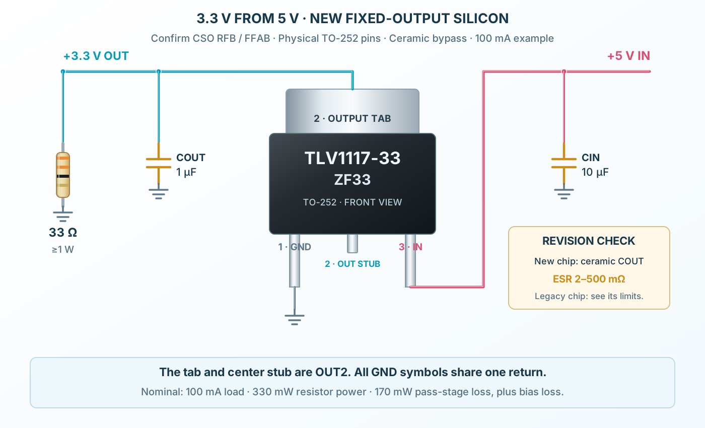
TLV1117-33 in a circuit
TO-252 physical connections and ceramic bypass.
Connect it, step by step
Follow the component values and pin connections
Supply
Apply 5 V to IN3; connect GND1 to the common return.
Bypass
Use local 10 µF input and 1 µF effective output ceramic capacitors.
Load
The 33 Ω load draws nominally 100 mA. The exposed tab is OUT2.
Inside TLV1117-33
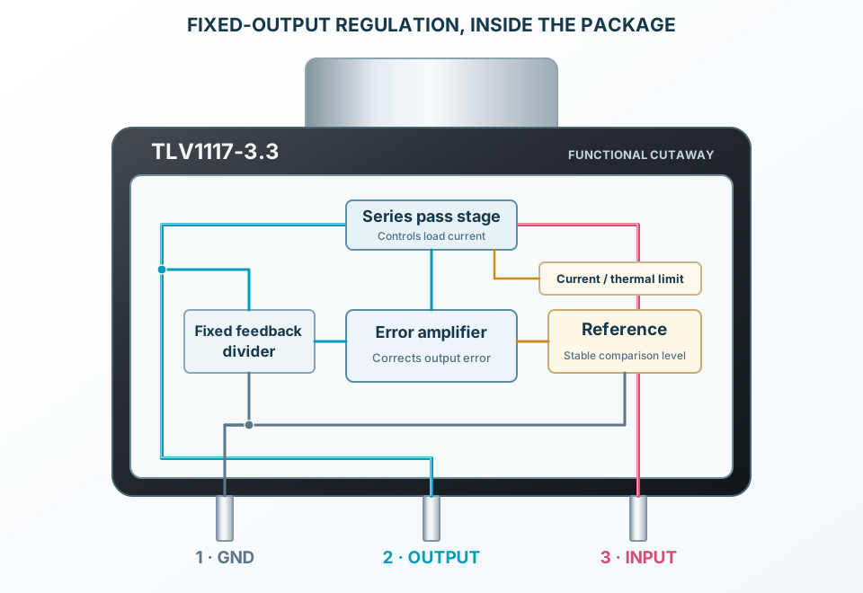
A compact reference, pass stage and feedback loop inside the package.
Explore the circuit
Select a stage to see its role and connections
Compare
Compare divided output voltage against the internal reference.
Regulate
Change pass-device drive to correct the error.
Protect
Limit overload and excessive junction temperature.
Selected packageTO-252TLV1117-33IKVURG3
Physical connections3 pinsPackage-specific numbering
Reference collection7 tables38 parameters & pin functions
Pin reference
Signal names, electrical functions and connection guidance
Physical pin numbers3 pins
Scroll within the table to see all columns and rows.
| Pin | Signal | Type | Function & connection |
|---|---|---|---|
| GND | Ground reference | Reference and bias return for the fixed 3.3 V regulator.Connection guidanceJoin input return, capacitor returns and load ground locally. Lead 1. The tab is OUTPUT, not ground. | |
| OUT | Regulated output and tab | Fixed 3.3 V output; also connected to the large exposed tab.Connection guidanceConnect the load and output stability capacitor here. Lead 2 and exposed thermal tab are one electrical node. | |
| IN | Supply input | Input to the protected series-pass stage.Connection guidanceUse +5 V with local ceramic bypass in the illustrated circuit. Recommended 4.7–15 V for this output; allow dropout and ripple margin. |
No pins match these filters. Try another signal name or reset the filters.
Exact order and silicon revision
One verified fixed-3.3 V package
Manufacturer-referenced values6 parameters
Scroll within the table to see all columns and rows.
| Parameter | Value | Conditions / notes |
|---|---|---|
| Selected order | TLV1117-33IKVURG3 | TO-252 KVU; industrial junction range |
| Package marking | ZF33 | Manufacturer marking plus traceability data |
| Physical electrical nodes | 1 GND; 2 OUT/tab; 3 IN | Metal tab must not be grounded |
| Legacy chip identifier | CSO SFB | Use legacy limits and stability guidance |
| New chip identifiers | CSO RFB or FFAB | Use new fixed-output specifications |
| Through-hole option | Not offered on this page | No matching fixed-3.3 V through-hole order verified in the selected order table |
No specifications match. Try a parameter name or a unit.
Package illustrations show identity; use the shipment label to distinguish silicon.
Operating range and accuracy
Selected I-grade device
Manufacturer-referenced values8 parameters
Scroll within the table to see all columns and rows.
| Parameter | Value | Conditions / notes |
|---|---|---|
| Recommended input | 4.7–15 V | Add ripple margin above worst-case dropout |
| Absolute maximum input | 16 V | Stress rating only |
| Output current | 0–800 mA | Limited by heat and source headroom |
| Recommended junction | −40 to 125°C | Not the ambient-temperature rating |
| Output at 25°C | 3.267–3.333 V | VIN5 V, 10 mA load |
| I-grade output over specified range | 3.168–3.432 V | VIN4.75–10 V; 0–800 mA; full temperature |
| I-grade line regulation | 1 mV typical; 10 mV maximum | VIN4.75–15 V, no load |
| I-grade load regulation | 1 mV typical; 15 mV maximum | VIN4.75 V; 0–800 mA |
No specifications match. Try a parameter name or a unit.
C-grade temperature and accuracy limits are not substituted.
Dropout: legacy versus new
I-grade limits; load matters
Manufacturer-referenced values6 parameters
Scroll within the table to see all columns and rows.
| Parameter | Value | Conditions / notes |
|---|---|---|
| Legacy at 100 mA | 1.1 V typical; 1.3 V maximum | Output dropout test |
| Legacy at 500 mA | 1.15 V typical; 1.35 V maximum | Output dropout test |
| Legacy at 800 mA | 1.2 V typical; 1.4 V maximum | Output dropout test |
| New fixed chip at 100 mA | 0.2 V typical; 0.4 V maximum | New-chip specification |
| New fixed chip at 500 mA | 0.5 V typical; 0.8 V maximum | New-chip specification |
| New fixed chip at 800 mA | 0.8 V typical; 1.2 V maximum | New-chip specification |
No specifications match. Try a parameter name or a unit.
The family operating input range still applies; dropout alone does not define the minimum permitted input.
Ground current and protection
Do not mix the silicon columns
Manufacturer-referenced values6 parameters
Scroll within the table to see all columns and rows.
| Parameter | Value | Conditions / notes |
|---|---|---|
| Legacy fixed-output ground current | 5 mA typical; 15 mA maximum | VIN≤15 V |
| New fixed no-load ground current | 65 µA typical; 110 µA maximum | VIN15 V; not a full-load bias specification |
| Legacy current limit | 0.8 A min.; 1.2 A typ.; 1.6 A max. | 5 V input/output differential, 25°C |
| New fixed current limit | 1.1 A typical; 1.6 A maximum | VOUT=90% nominal; specified input headroom |
| New fixed short-circuit current | 150–350 mA; 250 mA typical | Foldback protection; not useful output power |
| New fixed thermal shutdown | 180°C typical; reset 160°C typical | Protection values, far above normal operating limits |
No specifications match. Try a parameter name or a unit.
Keep the junction below 125°C in normal service.
Capacitors and revision selection
The diagram targets new fixed-output silicon
Manufacturer-referenced values6 parameters
Scroll within the table to see all columns and rows.
| Parameter | Value | Conditions / notes |
|---|---|---|
| Illustrated input bypass | 10 µF ceramic | Close to IN and GND; choose voltage rating and effective capacitance |
| Illustrated output capacitor | 1 µF effective ceramic | TI new-chip example uses 1 µF |
| New fixed-output ESR | 2–500 mΩ | Recommended operating condition |
| Ceramic dielectric | X7R or X5R | Account for tolerance, temperature and DC bias |
| Legacy output capacitor | At least 10 µF tantalum | Follow the legacy stability guidance, not the new-chip example |
| Long input wiring | Use local input capacitance | Especially when source impedance exceeds 0.5 Ω |
No specifications match. Try a parameter name or a unit.
A nominal capacitor value does not guarantee its effective value under applied voltage.
Board cooling and calculated load
TO-252 soldered directly to a PCB
Manufacturer-referenced values6 parameters
Scroll within the table to see all columns and rows.
| Parameter | Value | Conditions / notes |
|---|---|---|
| New-chip KVU θJA | 67.2°C/W | TI reference-board thermal metric |
| Legacy KVU θJA | 50.9°C/W | Different silicon column and board-dependent metric |
| Example output load | 33 Ω →100 mA nominal | Load power 330 mW; use ≥1 W resistor |
| Example pass loss | (5−3.3)×0.1=170 mW | Add VIN×actual ground current |
| Full 800 mA pass loss at 5 V | 1.36 W | Before bias term; large heat rise in small copper areas |
| Approximate rise at 1.36 W | 91°C using 67.2°C/W | Board-dependent estimate, not a guaranteed temperature |
No specifications match. Try a parameter name or a unit.
The headline 800 mA rating is not a promise at arbitrary input voltage and ambient.
No matching rowsTry a pin name, parameter, unit or test condition, or reset the filters.
Board supply rails
Derive 3.3 V from a suitable higher DC supply with short bypass loops.
Manufacturer application guideExisting 1117-family boards
Check pin order, silicon revision and capacitors before substitution.
Manufacturer application guideModerate-current loads
Budget heat and transient response rather than relying only on the current rating.
Manufacturer application guideTake it into ProTech
Find TLV1117-33 in the Components Library to place its schematic symbol and connect its pins.
Reference page · circuit simulation model not yet availableOpen ProTech