Real View
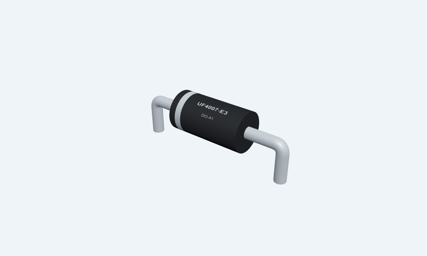
Fast recovery for controlled switching.
UF4007 is a two-terminal ultrafast silicon rectifier. Its glass-passivated PN junction passes forward current from anode to cathode and blocks reverse voltage within its limits. The band on the black axial body marks the cathode. This page follows Vishay’s 1000 V, 1 A DO-41 device. Unlike a general-purpose rectifier, it has a specified 75 ns maximum recovery time under the manufacturer’s test conditions. Switching frequency alone does not determine suitability: temperature, recovery current and circuit inductance matter too. An isolated 9 V RMS half-wave circuit demonstrates polarity and output shape at low voltage. Its fixed 0.7 V model is explanatory, not a guaranteed UF4007 drop. A slow bench circuit illustrates rectification; measuring nanosecond recovery requires appropriate high-bandwidth equipment.
Select a pin to explore its connection
Click a lead or use the arrow keys. Top view · band at K1 · A2 opposite
The banded end of the rectifier.
Connect to the positive half-wave output in the example.
This page uses the KiCad convention 1 = cathode, 2 = anode. The manufacturer identifies polarity by the band, not numeric package pins.
Conventional forward current enters here and leaves the cathode.
Connect to the isolated low-voltage AC source in the example.
Forward voltage depends on current and temperature; 0.7 V is only the teaching assumption used below.
The PN junction briefly carries reverse recovery current while stored charge is removed. The 75 ns limit belongs to a defined test; it is not a universal delay or a complete switching-loss model.
UF4007-E3 · DO-41
| Property | Details |
|---|---|
| Manufacturer | Vishay General Semiconductor |
| Part number | UF4007-E3 |
| Package | DO-41 |
| Connections | 2 pins |
| Mounting | Through-hole |
| Lead pitch | 10.16 mm · formed for this footprint |
| Package code | DO-204AL |
| Thermal reference | Rated current depends on lead length, copper and ambient temperature |
Vishay UF4007-E3 / M3
Scroll sideways to see all columns.
| Parameter | Value | Conditions / notes |
|---|---|---|
| Device | Ultrafast PN rectifier | Glass-passivated junction |
| Package | DO-41 / DO-204AL | Molded axial body |
| Cathode | Colored body band | Polarity does not depend on rotation |
| PCB numbering | 1 = K · 2 = A | Page / footprint convention |
| Lead finish | Matte tin plated | Silver-colored round leads |
| Ordering example | UF4007-E3/54 | Commercial tape and reel |
No specifications match. Try a parameter name or a unit.
An identical body does not make the electrical ratings identical to 1N4007.
Selected UF4007 column
Scroll sideways to see all columns.
| Parameter | Value | Conditions / notes |
|---|---|---|
| Repetitive reverse peak | 1000 V | VRRM |
| RMS reverse voltage | 700 V | VRMS |
| DC blocking voltage | 1000 V | VDC |
| Average rectified current | 1 A | 9.5 mm lead length; TA = 55°C |
| Surge current | 30 A | 8.3 ms single half-sine superimposed on rated load |
| Junction / storage range | −55 to +150°C | Absolute limits |
No specifications match. Try a parameter name or a unit.
Thermal derating and mounting conditions still apply; these limits are not simultaneous design targets.
25°C ambient unless stated
Scroll sideways to see all columns.
| Parameter | Value | Conditions / notes |
|---|---|---|
| Forward voltage | 1.7 V maximum | IF = 1 A; 300 µs pulse, 1% duty |
| Reverse leakage | 10 µA maximum | Rated blocking voltage; TA = 25°C |
| Hot reverse leakage | 50 µA maximum | Rated blocking voltage; TA = 100°C |
| Reverse recovery | 75 ns maximum | IF = 0.5 A; IR = 1 A; recovery endpoint Irr = 0.25 A |
| Junction capacitance | 17 pF typical | VR = 4 V; f = 1 MHz |
| Typical RθJA / RθJL | 60 / 15°C/W | Manufacturer’s stated lead/mounting conditions |
No specifications match. Try a parameter name or a unit.
The 1.7 V maximum is not the fixed 0.7 V teaching assumption used in the basic circuit.
DO-41 outline and authored lands
Scroll sideways to see all columns.
| Parameter | Value | Conditions / notes |
|---|---|---|
| Body length | 4.1–5.2 mm | Before lead forming |
| Body diameter | 2.0–2.7 mm | Molded body |
| Lead diameter | 0.71–0.86 mm | Plated wire |
| Straight lead length | 25.4 mm minimum per end | Before forming/cutting |
| Chosen mounting pitch | 10.16 mm | Authored layout choice |
| Pad / finished hole | 2.0 / 1.1 mm | Check actual leads and assembly clearance |
No specifications match. Try a parameter name or a unit.
The downloadable footprint is an engineering starting pattern, not a manufacturer-certified PCB layout.
Isolated supply; calculated values
Scroll sideways to see all columns.
| Parameter | Value | Conditions / notes |
|---|---|---|
| Input | 9 V RMS · 60 Hz | Isolated sine source |
| Load | 1 kΩ · 0.25 W or greater | Cathode to load positive |
| Assumed drop | 0.7 V | Fixed model only |
| Input peak | 12.73 V | 9 × √2 |
| Output peak | 12.03 V | Input peak minus assumed drop |
| Peak current | 12.03 mA | 12.03 V / 1 kΩ |
| Average output | Approximately 3.71 V | Unfiltered half-wave with conduction threshold |
| Recovery measurement | Not demonstrated by this slow circuit | Needs the defined test currents and fast measurement |
No specifications match. Try a parameter name or a unit.
Both ground symbols share the isolated source return.
Select a pin for its function, connection guidance and electrical notes.
Follow the labeled connections and functional stages
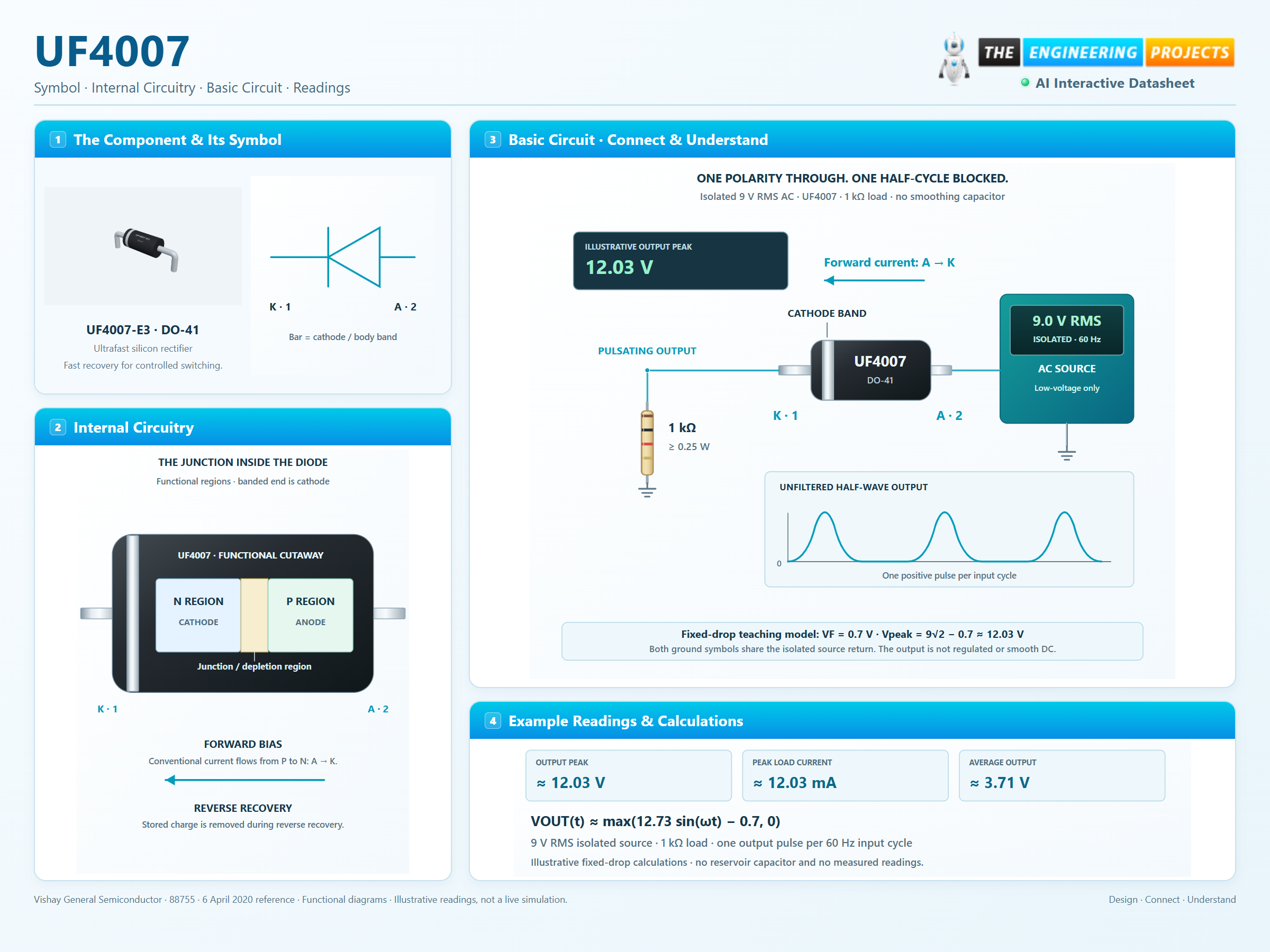
3 stages · Explore one step at a time
The banded end is cathode K, numbered 1 in this PCB convention.
The anode must be positive enough relative to cathode to forward-bias the junction.
With no filter capacitor, current returns to zero through each blocked half-cycle.
Physical diode, resistor and a clearly labelled low-voltage source.
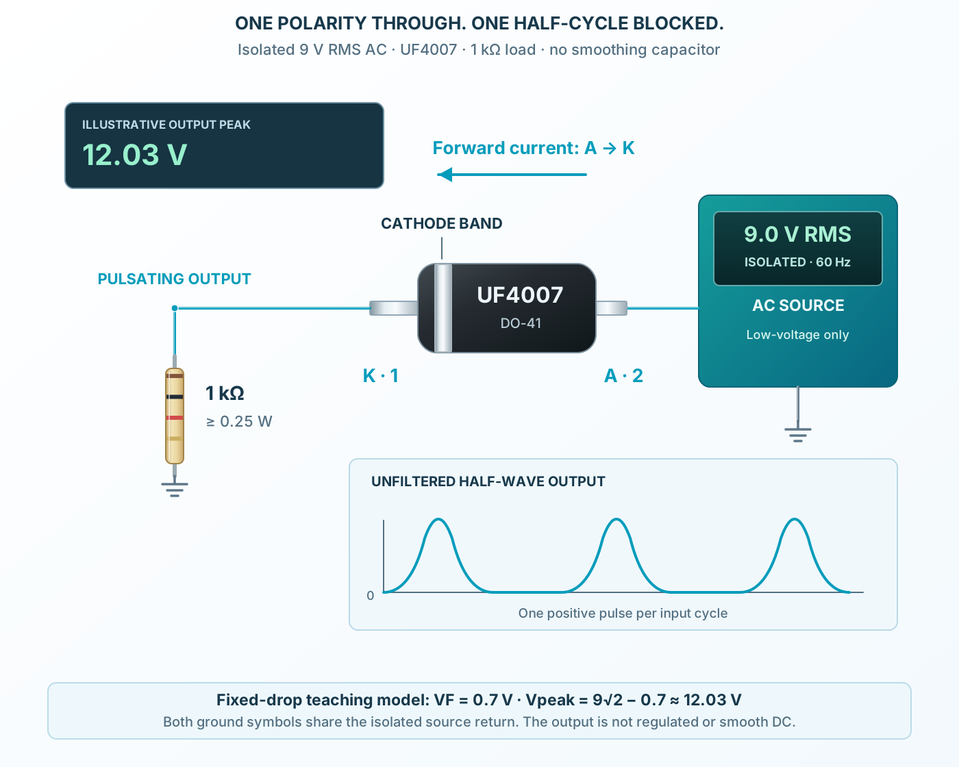
Follow the component values and pin connections
Use the isolated 9 V RMS source.
Connect anode to source and banded cathode to load.
Return the 1 kΩ resistor to the other source terminal.
A compact functional cutaway within the diode body.
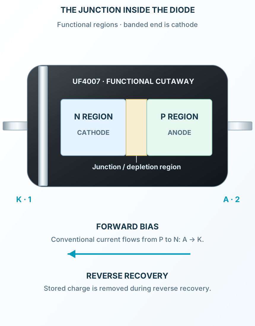
Select a stage to see its role and connections
Forward bias injects carriers into the junction.
Stored charge must be removed after the applied polarity reverses.
The 75 ns maximum is specified at IF = 0.5 A, IR = 1 A and Irr = 0.25 A.
Signal names, electrical functions and connection guidance
Scroll within the table to see all columns and rows.
| Pin | Signal | Type | Function & connection |
|---|---|---|---|
| K | Cathode | The banded end of the rectifier.Connection guidanceConnect to the positive half-wave output in the example. This page uses the KiCad convention 1 = cathode, 2 = anode. The manufacturer identifies polarity by the band, not numeric package pins. | |
| A | Anode | Conventional forward current enters here and leaves the cathode.Connection guidanceConnect to the isolated low-voltage AC source in the example. Forward voltage depends on current and temperature; 0.7 V is only the teaching assumption used below. |
No pins match these filters. Try another signal name or reset the filters.
Vishay UF4007-E3 / M3
Scroll within the table to see all columns and rows.
| Parameter | Value | Conditions / notes |
|---|---|---|
| Device | Ultrafast PN rectifier | Glass-passivated junction |
| Package | DO-41 / DO-204AL | Molded axial body |
| Cathode | Colored body band | Polarity does not depend on rotation |
| PCB numbering | 1 = K · 2 = A | Page / footprint convention |
| Lead finish | Matte tin plated | Silver-colored round leads |
| Ordering example | UF4007-E3/54 | Commercial tape and reel |
No specifications match. Try a parameter name or a unit.
An identical body does not make the electrical ratings identical to 1N4007.
Selected UF4007 column
Scroll within the table to see all columns and rows.
| Parameter | Value | Conditions / notes |
|---|---|---|
| Repetitive reverse peak | 1000 V | VRRM |
| RMS reverse voltage | 700 V | VRMS |
| DC blocking voltage | 1000 V | VDC |
| Average rectified current | 1 A | 9.5 mm lead length; TA = 55°C |
| Surge current | 30 A | 8.3 ms single half-sine superimposed on rated load |
| Junction / storage range | −55 to +150°C | Absolute limits |
No specifications match. Try a parameter name or a unit.
Thermal derating and mounting conditions still apply; these limits are not simultaneous design targets.
25°C ambient unless stated
Scroll within the table to see all columns and rows.
| Parameter | Value | Conditions / notes |
|---|---|---|
| Forward voltage | 1.7 V maximum | IF = 1 A; 300 µs pulse, 1% duty |
| Reverse leakage | 10 µA maximum | Rated blocking voltage; TA = 25°C |
| Hot reverse leakage | 50 µA maximum | Rated blocking voltage; TA = 100°C |
| Reverse recovery | 75 ns maximum | IF = 0.5 A; IR = 1 A; recovery endpoint Irr = 0.25 A |
| Junction capacitance | 17 pF typical | VR = 4 V; f = 1 MHz |
| Typical RθJA / RθJL | 60 / 15°C/W | Manufacturer’s stated lead/mounting conditions |
No specifications match. Try a parameter name or a unit.
The 1.7 V maximum is not the fixed 0.7 V teaching assumption used in the basic circuit.
DO-41 outline and authored lands
Scroll within the table to see all columns and rows.
| Parameter | Value | Conditions / notes |
|---|---|---|
| Body length | 4.1–5.2 mm | Before lead forming |
| Body diameter | 2.0–2.7 mm | Molded body |
| Lead diameter | 0.71–0.86 mm | Plated wire |
| Straight lead length | 25.4 mm minimum per end | Before forming/cutting |
| Chosen mounting pitch | 10.16 mm | Authored layout choice |
| Pad / finished hole | 2.0 / 1.1 mm | Check actual leads and assembly clearance |
No specifications match. Try a parameter name or a unit.
The downloadable footprint is an engineering starting pattern, not a manufacturer-certified PCB layout.
Isolated supply; calculated values
Scroll within the table to see all columns and rows.
| Parameter | Value | Conditions / notes |
|---|---|---|
| Input | 9 V RMS · 60 Hz | Isolated sine source |
| Load | 1 kΩ · 0.25 W or greater | Cathode to load positive |
| Assumed drop | 0.7 V | Fixed model only |
| Input peak | 12.73 V | 9 × √2 |
| Output peak | 12.03 V | Input peak minus assumed drop |
| Peak current | 12.03 mA | 12.03 V / 1 kΩ |
| Average output | Approximately 3.71 V | Unfiltered half-wave with conduction threshold |
| Recovery measurement | Not demonstrated by this slow circuit | Needs the defined test currents and fast measurement |
No specifications match. Try a parameter name or a unit.
Both ground symbols share the isolated source return.
No matching rowsTry a pin name, parameter, unit or test condition, or reset the filters.
Check reverse recovery, losses and circuit transients when selecting a rectifying path.
Manufacturer application guideCarry inductive load current within the voltage, current and thermal envelope.
Manufacturer application guideUse an isolated low-voltage source to observe one-polarity conduction.
Manufacturer application guideFind UF4007 in the Components Library to place its schematic symbol and connect its pins.
Reference page · circuit simulation model not yet availableOpen ProTech