Real View
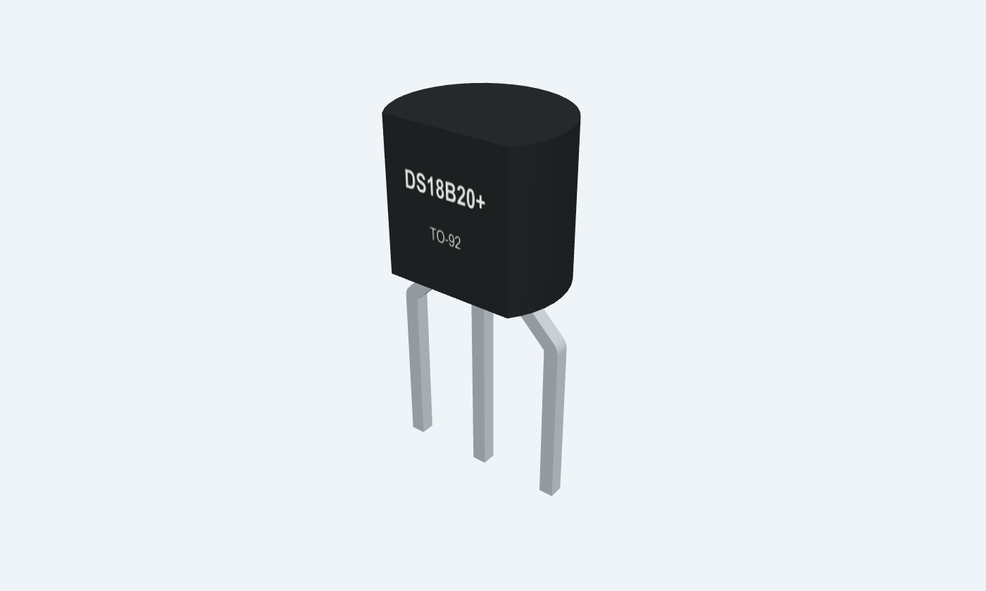
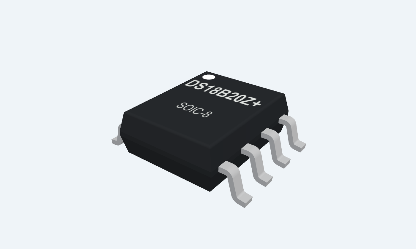
A temperature reading. A unique digital identity.
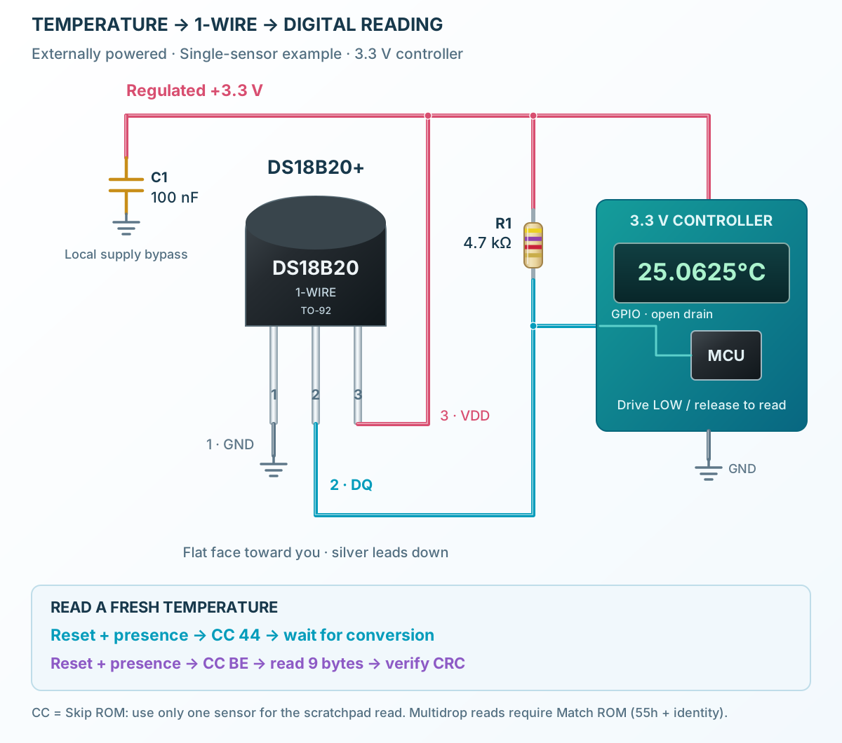
DS18B20 measures temperature digitally over a 1-Wire connection. Its programmable 9–12-bit conversion covers −55 to +125°C, with a stated ±0.5°C error band from −10 to +85°C. Resolution determines the smallest reported step; it does not replace the accuracy specification. Each sensor has a factory-programmed 64-bit ROM identity, allowing individually addressed sensors to share one bus. Temperature, alarm thresholds and configuration are read from a nine-byte scratchpad that includes a CRC. The views compare the three-lead DS18B20+ and the eight-lead DS18B20Z+ SOIC. Their physical pin numbers differ. The basic circuit uses external 3.3 V power, a shared ground and a pullup on DQ; parasite power has additional bus-power requirements.
Click a lead or use the arrow keys. Front view · flat face toward you
Supply and bus return.
Connect to the controller ground.
1-Wire commands and temperature data share this pin.
Connect to a controller open-drain GPIO and a 4.7 kΩ pullup.
Release the line to read HIGH; do not drive against another device. Parasite operation needs a strong pullup during conversion.
External supply for normal powered operation.
Connect to 3.0–5.5 V; tie to GND only when using parasite power.
The example uses a regulated 3.3 V supply and a 3.3 V data pullup.
SOIC physical pin 1 has no internal connection.
Leave unconnected.
SOIC physical pin 2 has no internal connection.
Leave unconnected.
SOIC physical pin 6 has no internal connection.
Leave unconnected.
SOIC physical pin 7 has no internal connection.
Leave unconnected.
SOIC physical pin 8 has no internal connection.
Leave unconnected.
1-Wire digital thermometer
The temperature converter writes a signed digital word. ROM addressing selects a sensor; the scratchpad provides the result, configuration and CRC.
DS18B20+
Key parameters and their test conditions
Follows the selected physical package
Select a pin to open its function, electrical notes and wiring guidance.
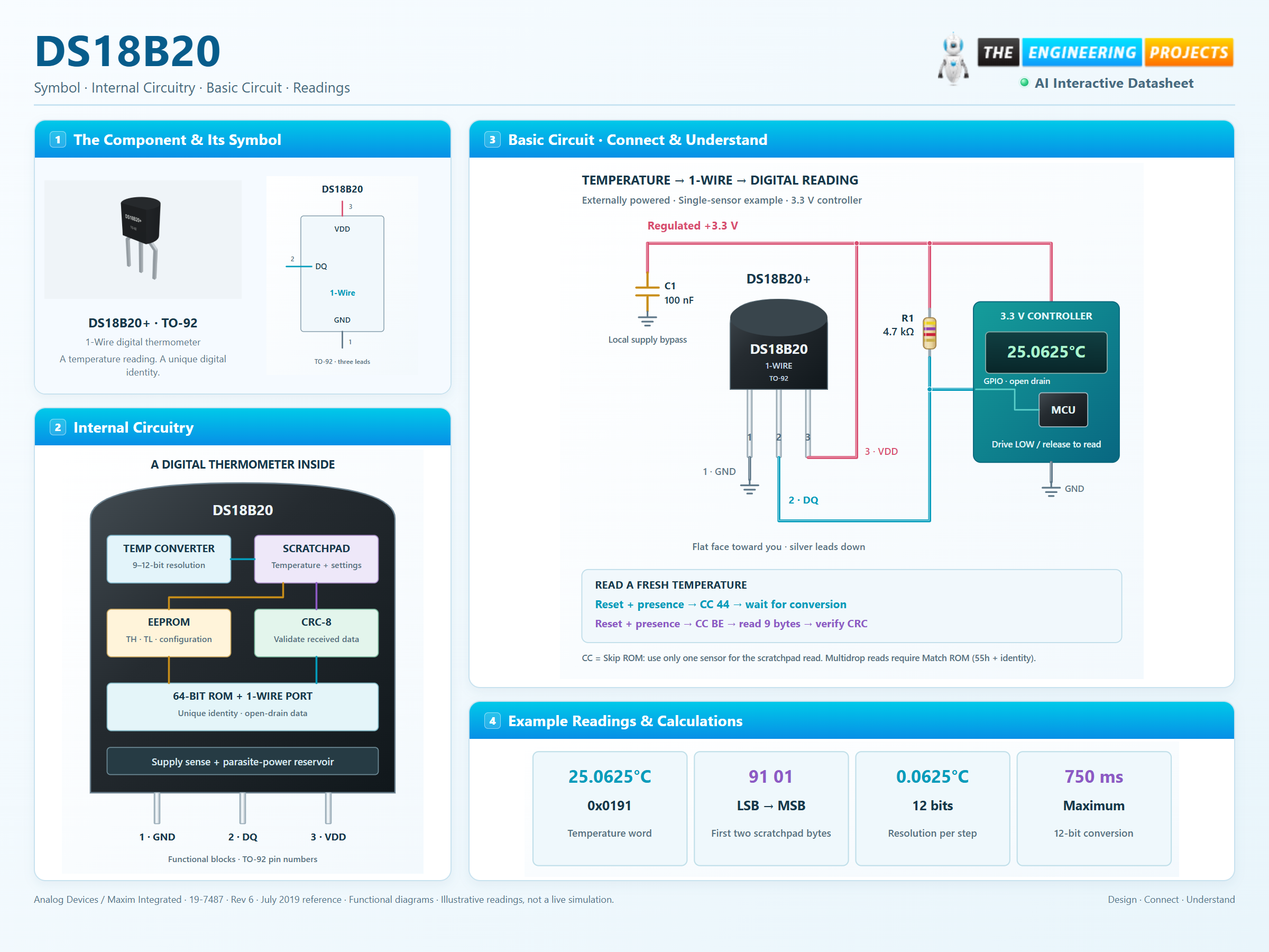
Reset the bus, detect presence and select the device using its 64-bit ROM identity. Skip ROM is suitable for a single-sensor read; multiple devices need individual addressing.
Issue Convert T (44h). Resolution changes the maximum time from 93.75 ms at 9 bits to 750 ms at 12 bits. Externally powered sensors can report completion in read slots.
Reset and select again, then Read Scratchpad (BEh). Read all nine bytes, verify CRC and decode the signed temperature word. Mask the undefined low bits at reduced resolution.
Read a completed conversion and verify its scratchpad CRC. A power-up register value of +85°C is not proof of a fresh temperature measurement. The calculator shows ideal register encoding, not sensor error or a timed 1-Wire bus.
Explore resolution and the signed 1-Wire temperature word.
These controls calculate a representative register value. A real sensor needs a Convert T command and time to complete a measurement.
—Scratchpad byte 0, then byte 1—Byte 4 · R1/R0 select resolutionDQ pin 2 uses an open-drain bus and pullup. Supply pin 3; ground pin 1. Ideal encoding only: temperature is rounded to the selected step. Undefined lower bits are displayed as zero. Alarm comparison discards fractional bits, including for negative temperatures. Verify CRC and conversion completion on real hardware.
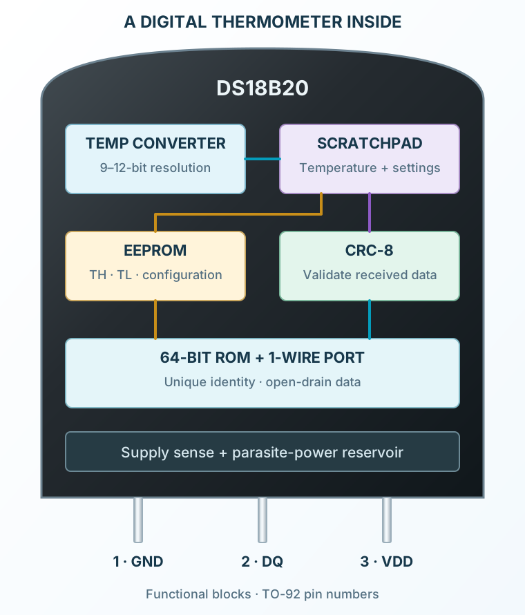
Select a pin to explore its function and connection.
| Pin | Signal | Type | Function |
|---|---|---|---|
| GND | Ground | Supply and bus return. | |
| DQ | Bidirectional, open-drain | 1-Wire commands and temperature data share this pin. | |
| VDD | Supply | External supply for normal powered operation. | |
| NC | Not connected | SOIC physical pin 1 has no internal connection. | |
| NC | Not connected | SOIC physical pin 2 has no internal connection. | |
| NC | Not connected | SOIC physical pin 6 has no internal connection. | |
| NC | Not connected | SOIC physical pin 7 has no internal connection. | |
| NC | Not connected | SOIC physical pin 8 has no internal connection. |
No pins match. Try a signal name or choose All pins.
DS18B20 · all selected packages
| Parameter | Value | Conditions / notes |
|---|---|---|
| External supply | 3.0–5.5 V | VDD relative to GND |
| Measurement range | −55 to +125°C | Externally powered operation |
| Error band, central range | ±0.5°C | −10 to +85°C |
| Error band, wider range | ±1°C | −30 to +100°C |
| Error band, full range | ±2°C | −55 to +125°C |
| DQ pullup, external power | 3.0 V to VDD | Example: 4.7 kΩ to 3.3 V |
| High-temperature operation | Use external power above +100°C | Parasite power is not recommended there |
No specifications match. Try a parameter name or a unit.
Manufacturer thermometer-error limits are 3-sigma values. A 0.0625°C step is not ±0.0625°C accuracy.
Configuration byte 4 · R1/R0
| Parameter | Value | Conditions / notes |
|---|---|---|
| 9 bits · R1/R0 = 00 | 0.5°C · 93.75 ms maximum | Configuration 1Fh; mask temperature bits 2:0 |
| 10 bits · R1/R0 = 01 | 0.25°C · 187.5 ms maximum | Configuration 3Fh; mask bits 1:0 |
| 11 bits · R1/R0 = 10 | 0.125°C · 375 ms maximum | Configuration 5Fh; mask bit 0 |
| 12 bits · R1/R0 = 11 | 0.0625°C · 750 ms maximum | Configuration 7Fh; all temperature bits valid |
| Power-up temperature word | 0550h = +85°C | Perform a conversion before treating it as a fresh reading |
No specifications match. Try a parameter name or a unit.
The page calculator rounds to a nominal representable value and displays masked low bits as zero. Hardware low bits below the selected resolution are undefined.
Bytes travel least-significant bit first
| Parameter | Value | Conditions / notes |
|---|---|---|
| Scratchpad bytes 0 and 1 | Temperature LSB, then MSB | Signed two’s-complement word; divide by 16 after masking |
| Byte 2 / byte 3 | TH / TL | Signed 8-bit integer alarm thresholds |
| Byte 4 | Resolution configuration | R1/R0 at bits 6:5; preserve reserved bit format |
| Bytes 5, 6 and 7 | Reserved | Read for CRC; do not assume all reserved values are fixed |
| Byte 8 | CRC-8 over bytes 0–7 | Polynomial x⁸ + x⁵ + x⁴ + 1; initial value zero |
| 64-bit ROM | 28h family + 48-bit serial + 8-bit CRC | Unique identity for bus addressing |
| Alarm comparison | Temperature bits 11:4 | Alarm when integer reading ≤ TL or ≥ TH |
No specifications match. Try a parameter name or a unit.
Alarm flags update after a conversion. The bus master must verify CRC; the device does not reject a host operation automatically when the host observes a mismatch.
Initialize → ROM command → function command
| Parameter | Value | Conditions / notes |
|---|---|---|
| Search ROM / Match ROM | F0h / 55h | Discover devices / select one 64-bit identity |
| Read ROM / Skip ROM | 33h / CCh | Read ROM only on a single-device bus; Skip addresses all |
| Alarm Search | ECh | Only sensors with an alarm flag participate |
| Convert T | 44h | Start one temperature conversion |
| Read Scratchpad | BEh | Read nine bytes including CRC |
| Write Scratchpad | 4Eh | Write TH, TL and configuration; complete all three bytes |
| Copy Scratchpad | 48h | Store alarm/configuration values in EEPROM |
| Recall EEPROM | B8h | Restore stored settings into scratchpad |
| Read Power Supply | B4h | Read slot: LOW = parasite, HIGH = external |
No specifications match. Try a parameter name or a unit.
Skip ROM followed by Read Scratchpad causes collisions when multiple devices respond. Use Match ROM for each sensor.
VDD = 3.0–5.5 V
| Parameter | Value | Conditions / notes |
|---|---|---|
| Reset LOW / reset HIGH | 480 µs minimum / 480 µs minimum | A parasite-powered reset LOW over 960 µs can cause a power-on reset |
| Presence wait / presence LOW | 15–60 µs / 60–240 µs | Measured after master releases reset |
| Time slot / recovery | 60–120 µs / at least 1 µs | Standard-speed transactions |
| Write-zero LOW | 60–120 µs | Hold the bus LOW for the slot |
| Write-one LOW | 1–15 µs | Release the bus for the rest of the slot |
| Read data valid | Within 15 µs | Sample within the specified read window |
| Strong pullup enable | Within 10 µs | After Convert T or Copy Scratchpad in parasite mode |
| EEPROM copy | 2 ms typical · 10 ms maximum | Keep required parasite pullup active |
No specifications match. Try a parameter name or a unit.
Conversion time and bus bit timing are separate. Releasing the line means high impedance, with the external resistor raising DQ.
Manufacturer test conditions
| Parameter | Value | Conditions / notes |
|---|---|---|
| Input LOW | −0.3 to +0.8 V | Low-voltage parasite presence may require ≤ 0.5 V |
| Input HIGH, external power | 2.2 V minimum | Observe upper input limit in the electrical table |
| Input HIGH, parasite power | 3.0 V minimum | Requires suitable pullup supply margin |
| LOW sink capability | 4 mA at 0.4 V | Open-drain interface |
| Standby current | 750 nA typical · 1 µA maximum | Specified to +70°C; typically 3 µA at +125°C |
| Conversion / EEPROM current | 1 mA typical · 1.5 mA maximum | VDD = 5 V |
| EEPROM endurance | 50,000 writes | −55 to +55°C |
| EEPROM retention | 10 years | −55 to +55°C |
| Any pin absolute stress | −0.5 to +6.0 V | Not a normal operating range |
No specifications match. Try a parameter name or a unit.
A weak pullup alone cannot supply the worst-case conversion current in parasite mode. Use a strong pullup for the full operation.
TO-92 and SOIC are not pin-for-pin equivalents
| Parameter | Value | Conditions / notes |
|---|---|---|
| GND | TO-92: 1 · SOIC: 5 | Common return |
| DQ | TO-92: 2 · SOIC: 4 | Bidirectional 1-Wire |
| VDD | TO-92: 3 · SOIC: 3 | External power or GND in parasite mode |
| Not connected | SOIC: 1, 2, 6, 7, 8 | Leave unused |
| Another family package | µSOP-8 also exists | Different pin map; not the SOIC view shown here |
No specifications match. Try a parameter name or a unit.
Check the selected order code and package orientation before wiring.
Give each sensor a stored ROM identity and read devices individually on a shared bus.
Manufacturer application guideUse programmable thresholds and Alarm Search to identify sensors outside a chosen band.
Manufacturer application guideRead a digital temperature word without using a microcontroller ADC channel.
Manufacturer application guideFind DS18B20 in the Components Library to place its schematic symbol and connect its pins.
Reference page · circuit simulation model not yet availableOpen ProTech