Real View
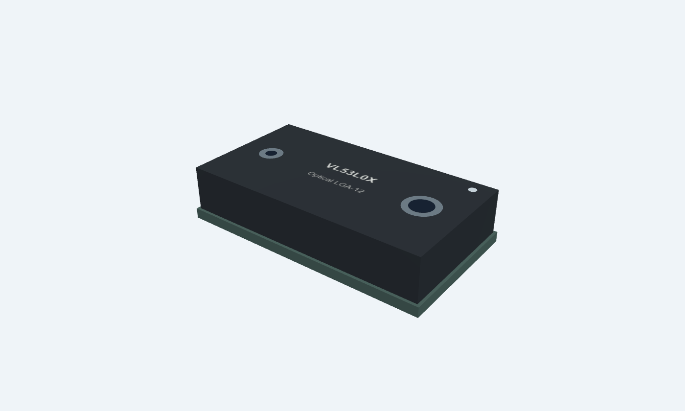
Measure distance from the flight time of invisible infrared light.
VL53L0X combines a 940 nm vertical-cavity laser, a single-photon avalanche-diode receiver and ranging electronics in a 4.4 × 2.4 mm optical package. It estimates distance using time of flight, then delivers a range result and validity status over I²C. The bare sensor uses 2.6–3.5 V power. It supports 1.8 V or supply-level I/O, selected during initialization; the example uses 2.8 V with the API configured for 2V8 mode. A breakout board may add regulation or level shifting, but those are not features of the bare package. Range depends on the selected timing budget, target reflectance and ambient infrared light. The 2 m profile is intended for dark conditions, not a guaranteed distance under sunlight. Use ST’s API, calibration and cover-glass guidance, and check measurement status before accepting a reading.
Select a pin to explore its connection
Click a lead or use the arrow keys. Top view · pin 1 bottom-right
Supply for the infrared VCSEL.
Connect to the main 2.6–3.5 V rail; bypass near pins 1 and 2.
Ground for the emitter supply.
Connect to the main ground plane.
Common ground contact.
Connect to the main ground plane.
Common ground contact.
Connect to the main ground plane.
LOW selects hardware standby.
Drive from the host; use a 10 kΩ pull-up when host state is unknown.
Never leave this input floating. Drive HIGH only with AVDD present.
Common ground contact.
Connect to the main ground plane.
Signals a programmed measurement event.
Use a 10 kΩ pull-up to the selected I/O rail and a host input. Leave open if unused.
Reserved internal contact.
Leave floating; do not connect to ground or power.
Bidirectional serial data.
Pull up to the configured I/O rail; 1.5–2 kΩ is ST’s example at 2.8 V / 400 kHz.
Clock input from the controller.
Use up to 400 kHz with a suitable pull-up.
Sensor supply.
Connect to the same 2.6–3.5 V rail as pin 1.
Common ground contact.
Connect to the main ground plane.
Infrared pulses illuminate the target. The receiver and timing engine estimate flight time; signal processing produces a distance and status for the host.
VL53L0X · Optical LGA-12
| Property | Details |
|---|---|
| Manufacturer | STMicroelectronics |
| Part number | VL53L0X |
| Package | Optical LGA-12 |
| Connections | 12 pins |
| Mounting | SMD |
| Lead pitch | 0.80 mm |
| Package code | LGA-12 |
| Thermal reference | −20°C to +70°C |
Bare sensor, not a regulated breakout module
Scroll sideways to see all columns.
| Parameter | Value | Conditions / notes |
|---|---|---|
| AVDD and AVDDVCSEL | 2.6–3.5 V | Connect to the same rail; nominal 2.8 V |
| Standard I/O mode | 1.6–1.9 V | 1.8 V nominal; API default mode |
| 2V8 I/O mode | 2.6–3.5 V | HIGH levels equal AVDD; configure via API |
| Ambient temperature | −20 to +70°C | Normal operating range |
| Active ranging current | 19 mA typical | 23°C / 2.8 V, default API, 33 ms budget |
| Peak current | Up to 40 mA | Including VCSEL |
| Hardware standby | 5 µA typical / 7 µA maximum | At stated nominal temperature and voltage |
| Absolute voltage limit | −0.5 to 3.6 V | AVDD and digital I/O; stress limit, not operating range |
No specifications match. Try a parameter name or a unit.
Provide supply capacity for peak current and place the bypass capacitors close to the emitter supply pins.
Typical examples from manufacturer Table 13
Scroll sideways to see all columns.
| Parameter | Value | Conditions / notes |
|---|---|---|
| Default | 30 ms | 1.2 m; accuracy depends on Table 12 test conditions |
| High accuracy | 200 ms | 1.2 m, better than ±3% under specified conditions |
| Long range | 33 ms | 2 m only in dark conditions without ambient IR |
| High speed | 20 ms | 1.2 m, ±5% under specified conditions |
| Interpretation | Budget is not a guaranteed sample period | Include host transfers and housekeeping |
| Validity | Check range status | Do not accept a numeric distance from a failed sample |
No specifications match. Try a parameter name or a unit.
Target reflectance, ambient light, cover glass and calibration affect performance.
Address notation and board connections
Scroll sideways to see all columns.
| Parameter | Value | Conditions / notes |
|---|---|---|
| Default address | 0x29 seven-bit | Datasheet 0x52 write / 0x53 read include the direction bit |
| Maximum SCL | 400 kHz | Use pull-ups for the selected I/O level |
| SDA / SCL pull-ups | 1.5–2 kΩ example | ST recommendation at AVDD=2.8 V and 400 kHz |
| XSHUT / GPIO1 pull-ups | 10 kΩ example | GPIO1 may be open when unused; XSHUT must be driven |
| Multiple sensors | Use separate XSHUT control lines | Enable one at a time and assign distinct addresses after each reset |
| Initialization | ST API required | This is not a simple analog distance-voltage output |
| DNC pin 8 | Leave floating | Do not use as ground or supply |
No specifications match. Try a parameter name or a unit.
The illustrated host uses 2.8 V-compatible I/O and enables the sensor’s 2V8 mode.
Keep the optical path clear
Scroll sideways to see all columns.
| Parameter | Value | Conditions / notes |
|---|---|---|
| Emitter | 940 nm VCSEL | Invisible infrared source |
| Receiver | SPAD array | Single-photon avalanche-diode technology |
| Package height | 1.0 mm nominal | 4.4 × 2.4 mm outline |
| Cover glass | Offset and crosstalk calibration | Follow ST optical-window and exclusion-cone guidance |
| Reference calibration | Follow API sequence | Required for the target design |
| Distance equation | d = c × t / 2 | Conceptual round-trip relation; internal algorithms handle timing |
| 500 mm illustration | About 3.34 ns round trip | Physics illustration, not an accessible host timer reading |
No specifications match. Try a parameter name or a unit.
Do not obscure either optical aperture with labels, paint or board hardware.
Bare-sensor application connections
Scroll sideways to see all columns.
| Parameter | Value | Conditions / notes |
|---|---|---|
| Supply | Pins 1 and 11 to 2.8 V | 100 nF and 4.7 µF close to emitter supply / return |
| Ground | Pins 2, 3, 4, 6 and 12 | Connect to a common ground plane |
| Bus | SDA9 and SCL10 | 1.8 kΩ pull-ups to 2.8 V in this example |
| Shutdown | XSHUT5 with 10 kΩ pull-up | Host can pull LOW for hardware standby |
| Interrupt | GPIO1 pin 7 with 10 kΩ pull-up | Optional host input |
| Reserved | DNC8 floating | No connection |
| Mode | 2V8 API configuration | Use matching host logic levels |
No specifications match. Try a parameter name or a unit.
No 5 V tolerance or onboard regulator is assumed.
Select a pin for its function, connection guidance and electrical notes.
Follow the labeled connections and functional stages
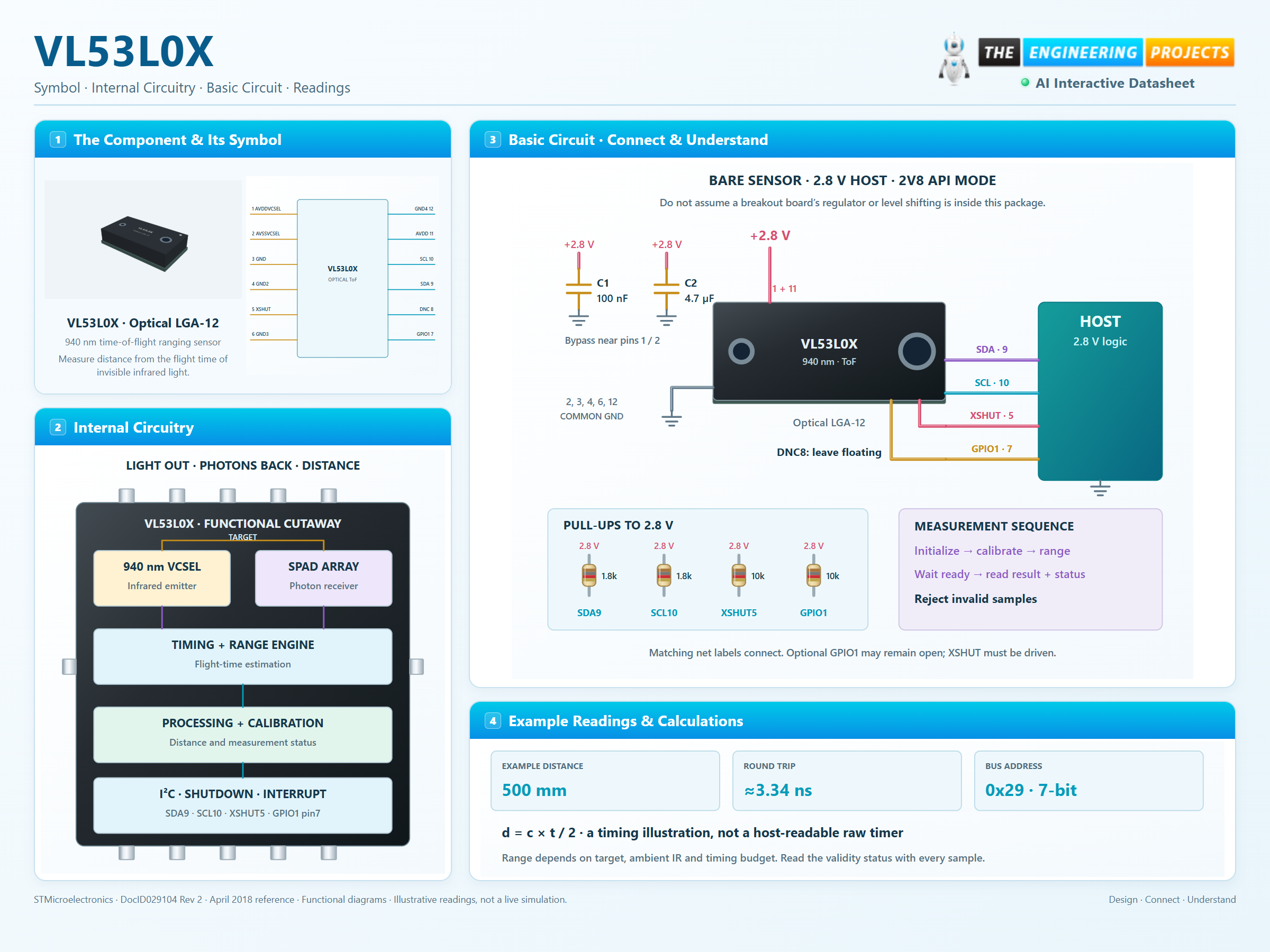
3 stages · Explore one step at a time
Use ST’s API to initialize the sensor and apply required reference, offset and cover-glass calibration.
The emitter and receiver collect timing information during the chosen measurement budget.
Wait for data-ready, read the result and clear the interrupt. Reject invalid or out-of-range samples.
Power, I²C, shutdown and optional interrupt.
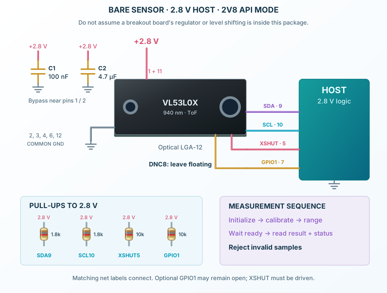
Follow the component values and pin connections
Connect both supplies and all five ground contacts.
Fit pull-ups, drive XSHUT and connect the I²C host.
Initialize, calibrate, start ranging and verify result status.
Optical timing and signal processing inside the module.
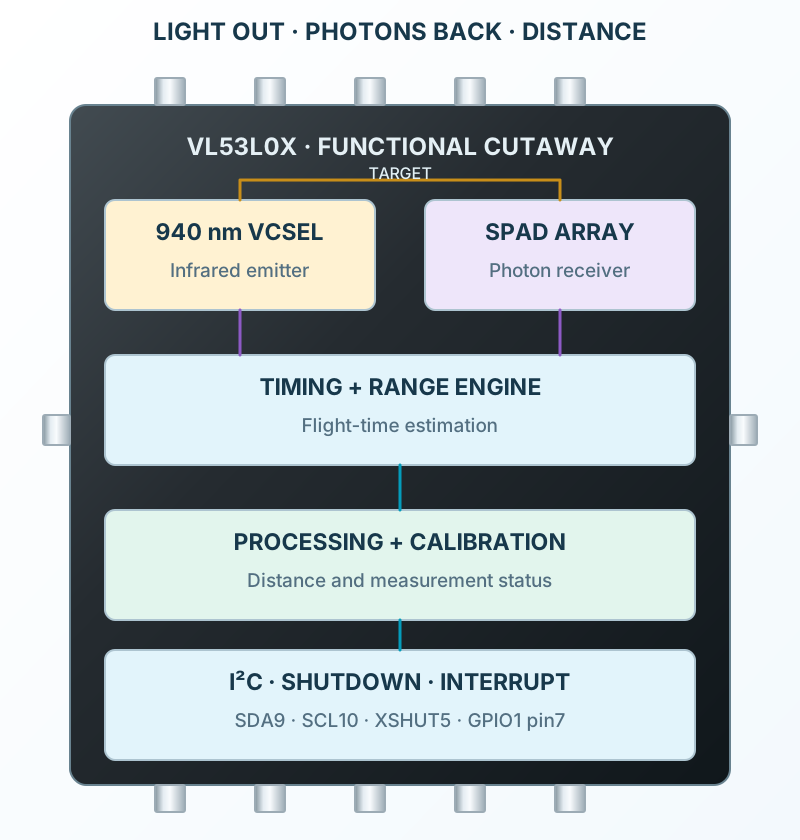
Select a stage to see its role and connections
A 940 nm VCSEL sends infrared pulses.
The SPAD array detects returning photons.
Timing and processing yield distance and validity status.
Signal names, electrical functions and connection guidance
Scroll within the table to see all columns and rows.
| Pin | Signal | Type | Function & connection |
|---|---|---|---|
| AVDDVCSEL | Emitter supply | Supply for the infrared VCSEL.Connection guidanceConnect to the main 2.6–3.5 V rail; bypass near pins 1 and 2. | |
| AVSSVCSEL | Emitter return | Ground for the emitter supply.Connection guidanceConnect to the main ground plane. | |
| GND | Ground | Common ground contact.Connection guidanceConnect to the main ground plane. | |
| GND2 | Ground | Common ground contact.Connection guidanceConnect to the main ground plane. | |
| XSHUT | Active-low shutdown | LOW selects hardware standby.Connection guidanceDrive from the host; use a 10 kΩ pull-up when host state is unknown. Never leave this input floating. Drive HIGH only with AVDD present. | |
| GND3 | Ground | Common ground contact.Connection guidanceConnect to the main ground plane. | |
| GPIO1 | Open-drain interrupt | Signals a programmed measurement event.Connection guidanceUse a 10 kΩ pull-up to the selected I/O rail and a host input. Leave open if unused. | |
| DNC | Do not connect | Reserved internal contact.Connection guidanceLeave floating; do not connect to ground or power. | |
| SDA | I²C data | Bidirectional serial data.Connection guidancePull up to the configured I/O rail; 1.5–2 kΩ is ST’s example at 2.8 V / 400 kHz. | |
| SCL | I²C clock | Clock input from the controller.Connection guidanceUse up to 400 kHz with a suitable pull-up. | |
| AVDD | Main supply | Sensor supply.Connection guidanceConnect to the same 2.6–3.5 V rail as pin 1. | |
| GND4 | Ground | Common ground contact.Connection guidanceConnect to the main ground plane. |
No pins match these filters. Try another signal name or reset the filters.
Bare sensor, not a regulated breakout module
Scroll within the table to see all columns and rows.
| Parameter | Value | Conditions / notes |
|---|---|---|
| AVDD and AVDDVCSEL | 2.6–3.5 V | Connect to the same rail; nominal 2.8 V |
| Standard I/O mode | 1.6–1.9 V | 1.8 V nominal; API default mode |
| 2V8 I/O mode | 2.6–3.5 V | HIGH levels equal AVDD; configure via API |
| Ambient temperature | −20 to +70°C | Normal operating range |
| Active ranging current | 19 mA typical | 23°C / 2.8 V, default API, 33 ms budget |
| Peak current | Up to 40 mA | Including VCSEL |
| Hardware standby | 5 µA typical / 7 µA maximum | At stated nominal temperature and voltage |
| Absolute voltage limit | −0.5 to 3.6 V | AVDD and digital I/O; stress limit, not operating range |
No specifications match. Try a parameter name or a unit.
Provide supply capacity for peak current and place the bypass capacitors close to the emitter supply pins.
Typical examples from manufacturer Table 13
Scroll within the table to see all columns and rows.
| Parameter | Value | Conditions / notes |
|---|---|---|
| Default | 30 ms | 1.2 m; accuracy depends on Table 12 test conditions |
| High accuracy | 200 ms | 1.2 m, better than ±3% under specified conditions |
| Long range | 33 ms | 2 m only in dark conditions without ambient IR |
| High speed | 20 ms | 1.2 m, ±5% under specified conditions |
| Interpretation | Budget is not a guaranteed sample period | Include host transfers and housekeeping |
| Validity | Check range status | Do not accept a numeric distance from a failed sample |
No specifications match. Try a parameter name or a unit.
Target reflectance, ambient light, cover glass and calibration affect performance.
Address notation and board connections
Scroll within the table to see all columns and rows.
| Parameter | Value | Conditions / notes |
|---|---|---|
| Default address | 0x29 seven-bit | Datasheet 0x52 write / 0x53 read include the direction bit |
| Maximum SCL | 400 kHz | Use pull-ups for the selected I/O level |
| SDA / SCL pull-ups | 1.5–2 kΩ example | ST recommendation at AVDD=2.8 V and 400 kHz |
| XSHUT / GPIO1 pull-ups | 10 kΩ example | GPIO1 may be open when unused; XSHUT must be driven |
| Multiple sensors | Use separate XSHUT control lines | Enable one at a time and assign distinct addresses after each reset |
| Initialization | ST API required | This is not a simple analog distance-voltage output |
| DNC pin 8 | Leave floating | Do not use as ground or supply |
No specifications match. Try a parameter name or a unit.
The illustrated host uses 2.8 V-compatible I/O and enables the sensor’s 2V8 mode.
Keep the optical path clear
Scroll within the table to see all columns and rows.
| Parameter | Value | Conditions / notes |
|---|---|---|
| Emitter | 940 nm VCSEL | Invisible infrared source |
| Receiver | SPAD array | Single-photon avalanche-diode technology |
| Package height | 1.0 mm nominal | 4.4 × 2.4 mm outline |
| Cover glass | Offset and crosstalk calibration | Follow ST optical-window and exclusion-cone guidance |
| Reference calibration | Follow API sequence | Required for the target design |
| Distance equation | d = c × t / 2 | Conceptual round-trip relation; internal algorithms handle timing |
| 500 mm illustration | About 3.34 ns round trip | Physics illustration, not an accessible host timer reading |
No specifications match. Try a parameter name or a unit.
Do not obscure either optical aperture with labels, paint or board hardware.
Bare-sensor application connections
Scroll within the table to see all columns and rows.
| Parameter | Value | Conditions / notes |
|---|---|---|
| Supply | Pins 1 and 11 to 2.8 V | 100 nF and 4.7 µF close to emitter supply / return |
| Ground | Pins 2, 3, 4, 6 and 12 | Connect to a common ground plane |
| Bus | SDA9 and SCL10 | 1.8 kΩ pull-ups to 2.8 V in this example |
| Shutdown | XSHUT5 with 10 kΩ pull-up | Host can pull LOW for hardware standby |
| Interrupt | GPIO1 pin 7 with 10 kΩ pull-up | Optional host input |
| Reserved | DNC8 floating | No connection |
| Mode | 2V8 API configuration | Use matching host logic levels |
No specifications match. Try a parameter name or a unit.
No 5 V tolerance or onboard regulator is assumed.
No matching rowsTry a pin name, parameter, unit or test condition, or reset the filters.
Detect approach or distance with a compact optical module.
Manufacturer application guideMeasure nearby obstacles while respecting ambient-light and target limits.
Manufacturer application guideIntegrate ranging behind a suitable, calibrated optical window.
Manufacturer application guideFind VL53L0X in the Components Library to place its schematic symbol and connect its pins.
Reference page · circuit simulation model not yet availableOpen ProTech