Real View
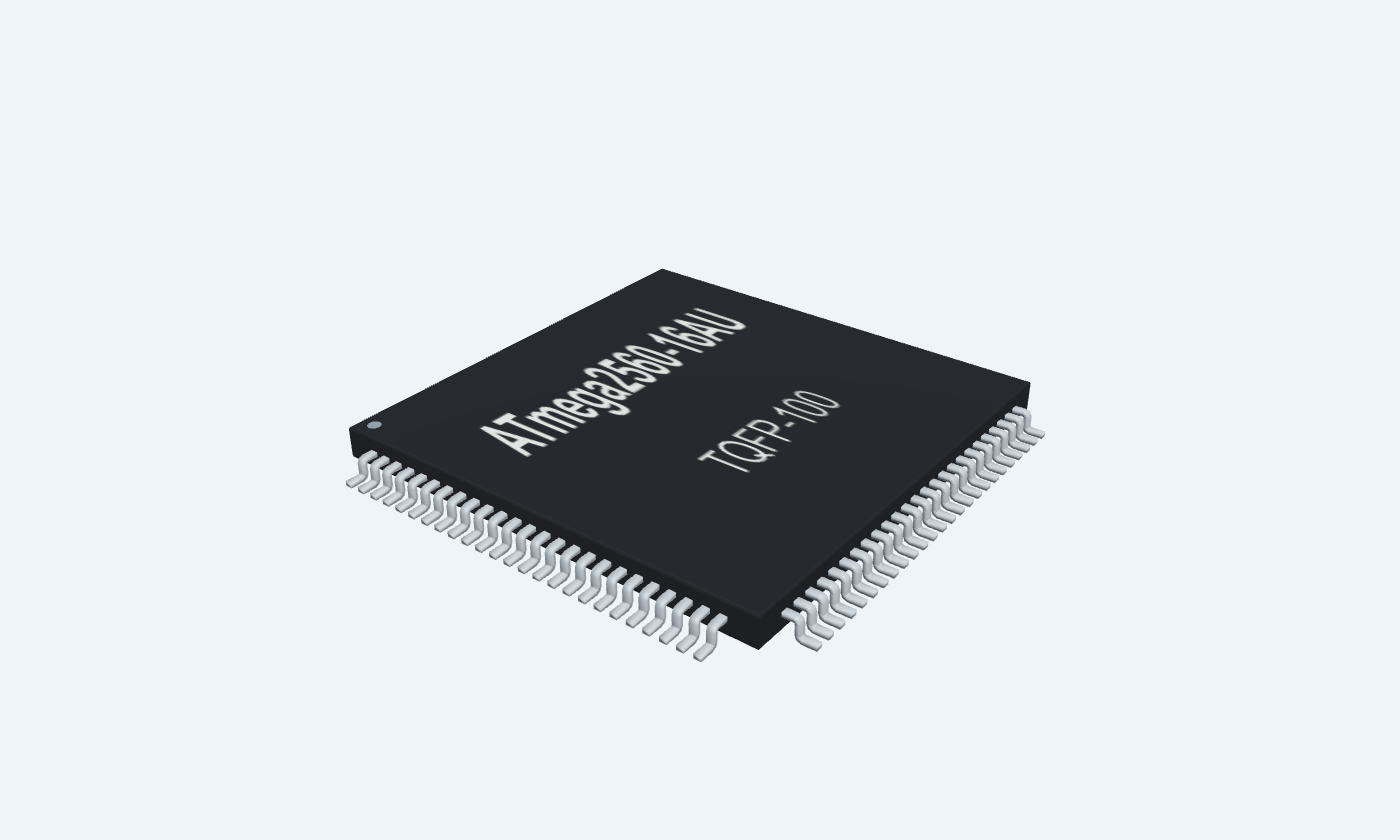
A large AVR with room for memory, ports and peripherals.
Microchip Technology / Atmel · ATmega2560-16AU
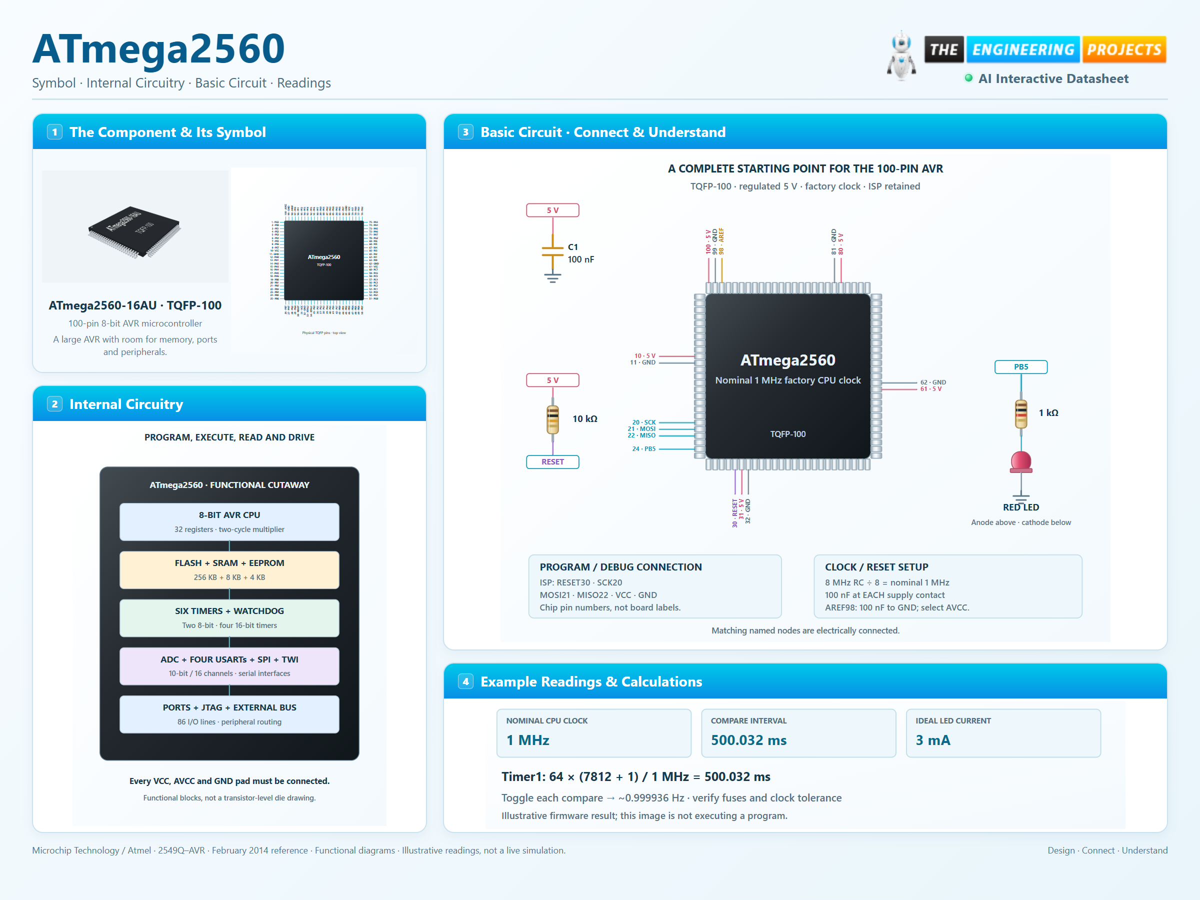
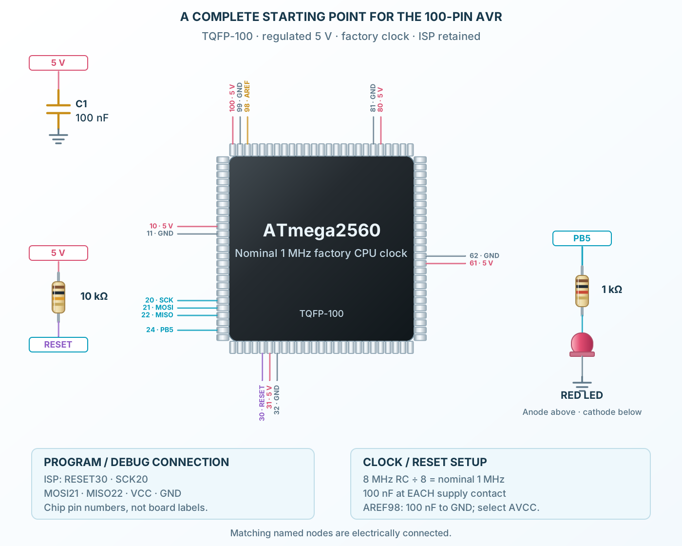
TQFP-1002549Q–AVR · February 2014ATmega2560 is an eight-bit AVR microcontroller with 256 KB of Flash, 8 KB of SRAM and 4 KB of EEPROM. Its 100-pin package provides 86 programmable I/O lines, four USARTs, six timer/counters and a sixteen-channel ten-bit ADC. The physical chip pin numbers shown here are separate from Arduino Mega board header labels. The selected ATmega2560-16AU operates from 4.5 to 5.5 V at up to 16 MHz. Low-voltage ATmega2560V parts have different limits. Clock-source and divider fuses determine the real CPU speed; a factory-configured part normally starts from its internal 8 MHz RC oscillator divided by eight. The basic circuit uses regulated 5 V and the nominal 1 MHz factory clock, so it needs no crystal for this demonstration. Every supply and ground is connected, ISP remains accessible and an LED is limited by 1 kΩ on PB5. Firmware must match the clock and configure the chosen output before a timing result is meaningful.
Click a lead or use the arrow keys. Top view
Port pad shared with the named hardware functions. Configure direction and peripheral selection.
Use voltage-compatible signals and define unused digital input levels.
Port pad shared with the named hardware functions. Configure direction and peripheral selection.
Use voltage-compatible signals and define unused digital input levels.
Port pad shared with the named hardware functions. Configure direction and peripheral selection.
Use voltage-compatible signals and define unused digital input levels.
Port pad shared with the named hardware functions. Configure direction and peripheral selection.
Use voltage-compatible signals and define unused digital input levels.
Port pad shared with the named hardware functions. Configure direction and peripheral selection.
Use voltage-compatible signals and define unused digital input levels.
Port pad shared with the named hardware functions. Configure direction and peripheral selection.
Use voltage-compatible signals and define unused digital input levels.
Port pad shared with the named hardware functions. Configure direction and peripheral selection.
Use voltage-compatible signals and define unused digital input levels.
Port pad shared with the named hardware functions. Configure direction and peripheral selection.
Use voltage-compatible signals and define unused digital input levels.
Port pad shared with the named hardware functions. Configure direction and peripheral selection.
Use voltage-compatible signals and define unused digital input levels.
Digital supply; all VCC pins must be connected.
Regulated 5 V with a nearby 100 nF bypass capacitor at each supply.
Ground return; connect every ground pad.
Common ground plane.
Port pad shared with the named hardware functions. Configure direction and peripheral selection.
Use voltage-compatible signals and define unused digital input levels.
Port pad shared with the named hardware functions. Configure direction and peripheral selection.
Use voltage-compatible signals and define unused digital input levels.
Port pad shared with the named hardware functions. Configure direction and peripheral selection.
Use voltage-compatible signals and define unused digital input levels.
Port pad shared with the named hardware functions. Configure direction and peripheral selection.
Use voltage-compatible signals and define unused digital input levels.
Port pad shared with the named hardware functions. Configure direction and peripheral selection.
Use voltage-compatible signals and define unused digital input levels.
Port pad shared with the named hardware functions. Configure direction and peripheral selection.
Use voltage-compatible signals and define unused digital input levels.
Port pad shared with the named hardware functions. Configure direction and peripheral selection.
Use voltage-compatible signals and define unused digital input levels.
Port pad shared with the named hardware functions. Configure direction and peripheral selection.
Use voltage-compatible signals and define unused digital input levels.
Keep SS configured appropriately when SPI operates as a controller.
Port pad shared with the named hardware functions. Configure direction and peripheral selection.
Route to a compatible ISP programmer; keep external loads from fighting programming signals.
Port pad shared with the named hardware functions. Configure direction and peripheral selection.
Route to a compatible ISP programmer; keep external loads from fighting programming signals.
Port pad shared with the named hardware functions. Configure direction and peripheral selection.
Route to a compatible ISP programmer; keep external loads from fighting programming signals.
Port pad shared with the named hardware functions. Configure direction and peripheral selection.
Use voltage-compatible signals and define unused digital input levels.
Port pad shared with the named hardware functions. Configure direction and peripheral selection.
Example LED through 1 kΩ to ground.
Port pad shared with the named hardware functions. Configure direction and peripheral selection.
Use voltage-compatible signals and define unused digital input levels.
Port pad shared with the named hardware functions. Configure direction and peripheral selection.
Use voltage-compatible signals and define unused digital input levels.
Port pad shared with the named hardware functions. Configure direction and peripheral selection.
Use voltage-compatible signals and define unused digital input levels.
Main oscillator or asynchronous timer oscillator connection, depending on the selected pin.
Use voltage-compatible signals and define unused digital input levels.
Main oscillator or asynchronous timer oscillator connection, depending on the selected pin.
Use voltage-compatible signals and define unused digital input levels.
Active-low reset and serial-programming entry.
10 kΩ pull-up to 5 V; route to ISP reset.
Digital supply; all VCC pins must be connected.
Regulated 5 V with a nearby 100 nF bypass capacitor at each supply.
Ground return; connect every ground pad.
Common ground plane.
Main oscillator or asynchronous timer oscillator connection, depending on the selected pin.
Use voltage-compatible signals and define unused digital input levels.
Main oscillator or asynchronous timer oscillator connection, depending on the selected pin.
Use voltage-compatible signals and define unused digital input levels.
Port pad shared with the named hardware functions. Configure direction and peripheral selection.
Use voltage-compatible signals and define unused digital input levels.
Port pad shared with the named hardware functions. Configure direction and peripheral selection.
Use voltage-compatible signals and define unused digital input levels.
Port pad shared with the named hardware functions. Configure direction and peripheral selection.
Use voltage-compatible signals and define unused digital input levels.
Port pad shared with the named hardware functions. Configure direction and peripheral selection.
Use voltage-compatible signals and define unused digital input levels.
Port pad shared with the named hardware functions. Configure direction and peripheral selection.
Use voltage-compatible signals and define unused digital input levels.
Port pad shared with the named hardware functions. Configure direction and peripheral selection.
Use voltage-compatible signals and define unused digital input levels.
Port pad shared with the named hardware functions. Configure direction and peripheral selection.
Use voltage-compatible signals and define unused digital input levels.
Port pad shared with the named hardware functions. Configure direction and peripheral selection.
Use voltage-compatible signals and define unused digital input levels.
Port pad shared with the named hardware functions. Configure direction and peripheral selection.
Use voltage-compatible signals and define unused digital input levels.
Two-wire signals require external pull-ups to a compatible supply.
Port pad shared with the named hardware functions. Configure direction and peripheral selection.
Use voltage-compatible signals and define unused digital input levels.
Two-wire signals require external pull-ups to a compatible supply.
Port pad shared with the named hardware functions. Configure direction and peripheral selection.
Use voltage-compatible signals and define unused digital input levels.
Port pad shared with the named hardware functions. Configure direction and peripheral selection.
Use voltage-compatible signals and define unused digital input levels.
Port pad shared with the named hardware functions. Configure direction and peripheral selection.
Use voltage-compatible signals and define unused digital input levels.
Port pad shared with the named hardware functions. Configure direction and peripheral selection.
Use voltage-compatible signals and define unused digital input levels.
Port pad shared with the named hardware functions. Configure direction and peripheral selection.
Use voltage-compatible signals and define unused digital input levels.
Port pad shared with the named hardware functions. Configure direction and peripheral selection.
Use voltage-compatible signals and define unused digital input levels.
Port pad shared with the named hardware functions. Configure direction and peripheral selection.
Use voltage-compatible signals and define unused digital input levels.
Port pad shared with the named hardware functions. Configure direction and peripheral selection.
Use voltage-compatible signals and define unused digital input levels.
Port pad shared with the named hardware functions. Configure direction and peripheral selection.
Use voltage-compatible signals and define unused digital input levels.
Port pad shared with the named hardware functions. Configure direction and peripheral selection.
Use voltage-compatible signals and define unused digital input levels.
Port pad shared with the named hardware functions. Configure direction and peripheral selection.
Use voltage-compatible signals and define unused digital input levels.
Port pad shared with the named hardware functions. Configure direction and peripheral selection.
Use voltage-compatible signals and define unused digital input levels.
Port pad shared with the named hardware functions. Configure direction and peripheral selection.
Use voltage-compatible signals and define unused digital input levels.
Port pad shared with the named hardware functions. Configure direction and peripheral selection.
Use voltage-compatible signals and define unused digital input levels.
Port pad shared with the named hardware functions. Configure direction and peripheral selection.
Use voltage-compatible signals and define unused digital input levels.
Port pad shared with the named hardware functions. Configure direction and peripheral selection.
Use voltage-compatible signals and define unused digital input levels.
Digital supply; all VCC pins must be connected.
Regulated 5 V with a nearby 100 nF bypass capacitor at each supply.
Ground return; connect every ground pad.
Common ground plane.
Port pad shared with the named hardware functions. Configure direction and peripheral selection.
Use voltage-compatible signals and define unused digital input levels.
Port pad shared with the named hardware functions. Configure direction and peripheral selection.
Use voltage-compatible signals and define unused digital input levels.
Port pad shared with the named hardware functions. Configure direction and peripheral selection.
Use voltage-compatible signals and define unused digital input levels.
Port pad shared with the named hardware functions. Configure direction and peripheral selection.
Use voltage-compatible signals and define unused digital input levels.
Port pad shared with the named hardware functions. Configure direction and peripheral selection.
Use voltage-compatible signals and define unused digital input levels.
Port pad shared with the named hardware functions. Configure direction and peripheral selection.
Use voltage-compatible signals and define unused digital input levels.
Port pad shared with the named hardware functions. Configure direction and peripheral selection.
Use voltage-compatible signals and define unused digital input levels.
Port pad shared with the named hardware functions. Configure direction and peripheral selection.
Use voltage-compatible signals and define unused digital input levels.
Port pad shared with the named hardware functions. Configure direction and peripheral selection.
Use voltage-compatible signals and define unused digital input levels.
Port pad shared with the named hardware functions. Configure direction and peripheral selection.
Use voltage-compatible signals and define unused digital input levels.
Port pad shared with the named hardware functions. Configure direction and peripheral selection.
Use voltage-compatible signals and define unused digital input levels.
Port pad shared with the named hardware functions. Configure direction and peripheral selection.
Use voltage-compatible signals and define unused digital input levels.
Port pad shared with the named hardware functions. Configure direction and peripheral selection.
Use voltage-compatible signals and define unused digital input levels.
Port pad shared with the named hardware functions. Configure direction and peripheral selection.
Use voltage-compatible signals and define unused digital input levels.
Port pad shared with the named hardware functions. Configure direction and peripheral selection.
Use voltage-compatible signals and define unused digital input levels.
Port pad shared with the named hardware functions. Configure direction and peripheral selection.
Use voltage-compatible signals and define unused digital input levels.
Port pad shared with the named hardware functions. Configure direction and peripheral selection.
Use voltage-compatible signals and define unused digital input levels.
Digital supply; all VCC pins must be connected.
Regulated 5 V with a nearby 100 nF bypass capacitor at each supply.
Ground return; connect every ground pad.
Common ground plane.
Port pad shared with the named hardware functions. Configure direction and peripheral selection.
Use voltage-compatible signals and define unused digital input levels.
Port pad shared with the named hardware functions. Configure direction and peripheral selection.
Use voltage-compatible signals and define unused digital input levels.
Port pad shared with the named hardware functions. Configure direction and peripheral selection.
Use voltage-compatible signals and define unused digital input levels.
Port pad shared with the named hardware functions. Configure direction and peripheral selection.
Use voltage-compatible signals and define unused digital input levels.
Port pad shared with the named hardware functions. Configure direction and peripheral selection.
Use voltage-compatible signals and define unused digital input levels.
Port pad shared with the named hardware functions. Configure direction and peripheral selection.
Use voltage-compatible signals and define unused digital input levels.
Port pad shared with the named hardware functions. Configure direction and peripheral selection.
Use voltage-compatible signals and define unused digital input levels.
Port pad shared with the named hardware functions. Configure direction and peripheral selection.
Use voltage-compatible signals and define unused digital input levels.
Port pad shared with the named hardware functions. Configure direction and peripheral selection.
Use voltage-compatible signals and define unused digital input levels.
JTAG can override GPIO/ADC functions on PF4–PF7; configure JTAG deliberately.
Port pad shared with the named hardware functions. Configure direction and peripheral selection.
Use voltage-compatible signals and define unused digital input levels.
JTAG can override GPIO/ADC functions on PF4–PF7; configure JTAG deliberately.
Port pad shared with the named hardware functions. Configure direction and peripheral selection.
Use voltage-compatible signals and define unused digital input levels.
JTAG can override GPIO/ADC functions on PF4–PF7; configure JTAG deliberately.
Port pad shared with the named hardware functions. Configure direction and peripheral selection.
Use voltage-compatible signals and define unused digital input levels.
JTAG can override GPIO/ADC functions on PF4–PF7; configure JTAG deliberately.
Port pad shared with the named hardware functions. Configure direction and peripheral selection.
Use voltage-compatible signals and define unused digital input levels.
Port pad shared with the named hardware functions. Configure direction and peripheral selection.
Use voltage-compatible signals and define unused digital input levels.
Port pad shared with the named hardware functions. Configure direction and peripheral selection.
Use voltage-compatible signals and define unused digital input levels.
Port pad shared with the named hardware functions. Configure direction and peripheral selection.
Use voltage-compatible signals and define unused digital input levels.
ADC reference input or internal-reference decoupling, according to reference selection.
Example: 100 nF to ground; select AVCC reference before using the ADC.
Do not drive AREF externally while an incompatible internal reference is enabled.
Ground return; connect every ground pad.
Common ground plane.
Analog and associated port supply; connect even when the ADC is unused.
Regulated 5 V with a nearby 100 nF bypass capacitor at each supply.
100-pin 8-bit AVR microcontroller
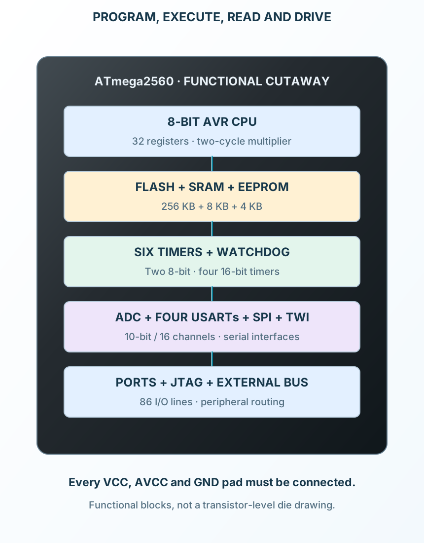
The AVR core shares memory with timers, serial interfaces and analog conversion. Pin multiplexing determines which function is connected to the board.
ATmega2560-16AU
Key parameters and their test conditions
Follows the selected physical package
Select a pin to open its function, electrical notes and wiring guidance.
Include AVCC and every digital supply/ground pair.
Check CKSEL and CKDIV8 before assuming the CPU frequency.
Keep RESET, SCK, MOSI, MISO and supply reference accessible.
At a nominal 1 MHz CPU clock, Timer1 CTC with prescaler 64 and OCR1A = 7812 gives a 500.032 ms compare interval. Toggle PB5 each interval for approximately 0.999936 Hz.
Select a pin to explore its function and connection.
| Pin | Signal | Type | Function |
|---|---|---|---|
| PG5 / OC0B | GPIO / peripheral | Port pad shared with the named hardware functions. Configure direction and peripheral selection. | |
| PE0 / RXD0 / PCINT8 | GPIO / peripheral | Port pad shared with the named hardware functions. Configure direction and peripheral selection. | |
| PE1 / TXD0 | GPIO / peripheral | Port pad shared with the named hardware functions. Configure direction and peripheral selection. | |
| PE2 / XCK0 / AIN0 | GPIO / peripheral | Port pad shared with the named hardware functions. Configure direction and peripheral selection. | |
| PE3 / OC3A / AIN1 | GPIO / peripheral | Port pad shared with the named hardware functions. Configure direction and peripheral selection. | |
| PE4 / OC3B / INT4 | GPIO / peripheral | Port pad shared with the named hardware functions. Configure direction and peripheral selection. | |
| PE5 / OC3C / INT5 | GPIO / peripheral | Port pad shared with the named hardware functions. Configure direction and peripheral selection. | |
| PE6 / T3 / INT6 | GPIO / peripheral | Port pad shared with the named hardware functions. Configure direction and peripheral selection. | |
| PE7 / CLKO / ICP3 / INT7 | GPIO / peripheral | Port pad shared with the named hardware functions. Configure direction and peripheral selection. | |
| VCC | Supply | Digital supply; all VCC pins must be connected. | |
| GND | Supply | Ground return; connect every ground pad. | |
| PH0 / RXD2 | GPIO / peripheral | Port pad shared with the named hardware functions. Configure direction and peripheral selection. | |
| PH1 / TXD2 | GPIO / peripheral | Port pad shared with the named hardware functions. Configure direction and peripheral selection. | |
| PH2 / XCK2 | GPIO / peripheral | Port pad shared with the named hardware functions. Configure direction and peripheral selection. | |
| PH3 / OC4A | GPIO / peripheral | Port pad shared with the named hardware functions. Configure direction and peripheral selection. | |
| PH4 / OC4B | GPIO / peripheral | Port pad shared with the named hardware functions. Configure direction and peripheral selection. | |
| PH5 / OC4C | GPIO / peripheral | Port pad shared with the named hardware functions. Configure direction and peripheral selection. | |
| PH6 / OC2B | GPIO / peripheral | Port pad shared with the named hardware functions. Configure direction and peripheral selection. | |
| PB0 / SS / PCINT0 | GPIO / peripheral | Port pad shared with the named hardware functions. Configure direction and peripheral selection. | |
| PB1 / SCK / PCINT1 | Program / debug | Port pad shared with the named hardware functions. Configure direction and peripheral selection. | |
| PB2 / MOSI / PCINT2 | Program / debug | Port pad shared with the named hardware functions. Configure direction and peripheral selection. | |
| PB3 / MISO / PCINT3 | Program / debug | Port pad shared with the named hardware functions. Configure direction and peripheral selection. | |
| PB4 / OC2A / PCINT4 | GPIO / peripheral | Port pad shared with the named hardware functions. Configure direction and peripheral selection. | |
| PB5 / OC1A / PCINT5 | GPIO / peripheral | Port pad shared with the named hardware functions. Configure direction and peripheral selection. | |
| PB6 / OC1B / PCINT6 | GPIO / peripheral | Port pad shared with the named hardware functions. Configure direction and peripheral selection. | |
| PB7 / OC0A / OC1C / PCINT7 | GPIO / peripheral | Port pad shared with the named hardware functions. Configure direction and peripheral selection. | |
| PH7 / T4 | GPIO / peripheral | Port pad shared with the named hardware functions. Configure direction and peripheral selection. | |
| PG3 / TOSC2 | Clock / GPIO | Main oscillator or asynchronous timer oscillator connection, depending on the selected pin. | |
| PG4 / TOSC1 | Clock / GPIO | Main oscillator or asynchronous timer oscillator connection, depending on the selected pin. | |
| RESET | Program / debug | Active-low reset and serial-programming entry. | |
| VCC | Supply | Digital supply; all VCC pins must be connected. | |
| GND | Supply | Ground return; connect every ground pad. | |
| XTAL2 | Clock / GPIO | Main oscillator or asynchronous timer oscillator connection, depending on the selected pin. | |
| XTAL1 | Clock / GPIO | Main oscillator or asynchronous timer oscillator connection, depending on the selected pin. | |
| PL0 / ICP4 | GPIO / peripheral | Port pad shared with the named hardware functions. Configure direction and peripheral selection. | |
| PL1 / ICP5 | GPIO / peripheral | Port pad shared with the named hardware functions. Configure direction and peripheral selection. | |
| PL2 / T5 | GPIO / peripheral | Port pad shared with the named hardware functions. Configure direction and peripheral selection. | |
| PL3 / OC5A | GPIO / peripheral | Port pad shared with the named hardware functions. Configure direction and peripheral selection. | |
| PL4 / OC5B | GPIO / peripheral | Port pad shared with the named hardware functions. Configure direction and peripheral selection. | |
| PL5 / OC5C | GPIO / peripheral | Port pad shared with the named hardware functions. Configure direction and peripheral selection. | |
| PL6 | GPIO / peripheral | Port pad shared with the named hardware functions. Configure direction and peripheral selection. | |
| PL7 | GPIO / peripheral | Port pad shared with the named hardware functions. Configure direction and peripheral selection. | |
| PD0 / SCL / INT0 | GPIO / peripheral | Port pad shared with the named hardware functions. Configure direction and peripheral selection. | |
| PD1 / SDA / INT1 | GPIO / peripheral | Port pad shared with the named hardware functions. Configure direction and peripheral selection. | |
| PD2 / RXD1 / INT2 | GPIO / peripheral | Port pad shared with the named hardware functions. Configure direction and peripheral selection. | |
| PD3 / TXD1 / INT3 | GPIO / peripheral | Port pad shared with the named hardware functions. Configure direction and peripheral selection. | |
| PD4 / ICP1 | GPIO / peripheral | Port pad shared with the named hardware functions. Configure direction and peripheral selection. | |
| PD5 / XCK1 | GPIO / peripheral | Port pad shared with the named hardware functions. Configure direction and peripheral selection. | |
| PD6 / T1 | GPIO / peripheral | Port pad shared with the named hardware functions. Configure direction and peripheral selection. | |
| PD7 / T0 | GPIO / peripheral | Port pad shared with the named hardware functions. Configure direction and peripheral selection. | |
| PG0 / WR | GPIO / peripheral | Port pad shared with the named hardware functions. Configure direction and peripheral selection. | |
| PG1 / RD | GPIO / peripheral | Port pad shared with the named hardware functions. Configure direction and peripheral selection. | |
| PC0 / A8 | GPIO / peripheral | Port pad shared with the named hardware functions. Configure direction and peripheral selection. | |
| PC1 / A9 | GPIO / peripheral | Port pad shared with the named hardware functions. Configure direction and peripheral selection. | |
| PC2 / A10 | GPIO / peripheral | Port pad shared with the named hardware functions. Configure direction and peripheral selection. | |
| PC3 / A11 | GPIO / peripheral | Port pad shared with the named hardware functions. Configure direction and peripheral selection. | |
| PC4 / A12 | GPIO / peripheral | Port pad shared with the named hardware functions. Configure direction and peripheral selection. | |
| PC5 / A13 | GPIO / peripheral | Port pad shared with the named hardware functions. Configure direction and peripheral selection. | |
| PC6 / A14 | GPIO / peripheral | Port pad shared with the named hardware functions. Configure direction and peripheral selection. | |
| PC7 / A15 | GPIO / peripheral | Port pad shared with the named hardware functions. Configure direction and peripheral selection. | |
| VCC | Supply | Digital supply; all VCC pins must be connected. | |
| GND | Supply | Ground return; connect every ground pad. | |
| PJ0 / RXD3 / PCINT9 | GPIO / peripheral | Port pad shared with the named hardware functions. Configure direction and peripheral selection. | |
| PJ1 / TXD3 / PCINT10 | GPIO / peripheral | Port pad shared with the named hardware functions. Configure direction and peripheral selection. | |
| PJ2 / XCK3 / PCINT11 | GPIO / peripheral | Port pad shared with the named hardware functions. Configure direction and peripheral selection. | |
| PJ3 / PCINT12 | GPIO / peripheral | Port pad shared with the named hardware functions. Configure direction and peripheral selection. | |
| PJ4 / PCINT13 | GPIO / peripheral | Port pad shared with the named hardware functions. Configure direction and peripheral selection. | |
| PJ5 / PCINT14 | GPIO / peripheral | Port pad shared with the named hardware functions. Configure direction and peripheral selection. | |
| PJ6 / PCINT15 | GPIO / peripheral | Port pad shared with the named hardware functions. Configure direction and peripheral selection. | |
| PG2 / ALE | GPIO / peripheral | Port pad shared with the named hardware functions. Configure direction and peripheral selection. | |
| PA7 / AD7 | GPIO / peripheral | Port pad shared with the named hardware functions. Configure direction and peripheral selection. | |
| PA6 / AD6 | GPIO / peripheral | Port pad shared with the named hardware functions. Configure direction and peripheral selection. | |
| PA5 / AD5 | GPIO / peripheral | Port pad shared with the named hardware functions. Configure direction and peripheral selection. | |
| PA4 / AD4 | GPIO / peripheral | Port pad shared with the named hardware functions. Configure direction and peripheral selection. | |
| PA3 / AD3 | GPIO / peripheral | Port pad shared with the named hardware functions. Configure direction and peripheral selection. | |
| PA2 / AD2 | GPIO / peripheral | Port pad shared with the named hardware functions. Configure direction and peripheral selection. | |
| PA1 / AD1 | GPIO / peripheral | Port pad shared with the named hardware functions. Configure direction and peripheral selection. | |
| PA0 / AD0 | GPIO / peripheral | Port pad shared with the named hardware functions. Configure direction and peripheral selection. | |
| PJ7 | GPIO / peripheral | Port pad shared with the named hardware functions. Configure direction and peripheral selection. | |
| VCC | Supply | Digital supply; all VCC pins must be connected. | |
| GND | Supply | Ground return; connect every ground pad. | |
| PK7 / ADC15 / PCINT23 | ADC / reference | Port pad shared with the named hardware functions. Configure direction and peripheral selection. | |
| PK6 / ADC14 / PCINT22 | ADC / reference | Port pad shared with the named hardware functions. Configure direction and peripheral selection. | |
| PK5 / ADC13 / PCINT21 | ADC / reference | Port pad shared with the named hardware functions. Configure direction and peripheral selection. | |
| PK4 / ADC12 / PCINT20 | ADC / reference | Port pad shared with the named hardware functions. Configure direction and peripheral selection. | |
| PK3 / ADC11 / PCINT19 | ADC / reference | Port pad shared with the named hardware functions. Configure direction and peripheral selection. | |
| PK2 / ADC10 / PCINT18 | ADC / reference | Port pad shared with the named hardware functions. Configure direction and peripheral selection. | |
| PK1 / ADC9 / PCINT17 | ADC / reference | Port pad shared with the named hardware functions. Configure direction and peripheral selection. | |
| PK0 / ADC8 / PCINT16 | ADC / reference | Port pad shared with the named hardware functions. Configure direction and peripheral selection. | |
| PF7 / ADC7 / TDI | ADC / reference | Port pad shared with the named hardware functions. Configure direction and peripheral selection. | |
| PF6 / ADC6 / TDO | ADC / reference | Port pad shared with the named hardware functions. Configure direction and peripheral selection. | |
| PF5 / ADC5 / TMS | ADC / reference | Port pad shared with the named hardware functions. Configure direction and peripheral selection. | |
| PF4 / ADC4 / TCK | ADC / reference | Port pad shared with the named hardware functions. Configure direction and peripheral selection. | |
| PF3 / ADC3 | ADC / reference | Port pad shared with the named hardware functions. Configure direction and peripheral selection. | |
| PF2 / ADC2 | ADC / reference | Port pad shared with the named hardware functions. Configure direction and peripheral selection. | |
| PF1 / ADC1 | ADC / reference | Port pad shared with the named hardware functions. Configure direction and peripheral selection. | |
| PF0 / ADC0 | ADC / reference | Port pad shared with the named hardware functions. Configure direction and peripheral selection. | |
| AREF | ADC / reference | ADC reference input or internal-reference decoupling, according to reference selection. | |
| GND | Supply | Ground return; connect every ground pad. | |
| AVCC | Supply | Analog and associated port supply; connect even when the ADC is unused. |
No pins match. Try a signal name or choose All pins.
Selected ATmega2560
| Parameter | Value | Conditions / notes |
|---|---|---|
| Program Flash | 256 KB | 128K 16-bit instruction words |
| SRAM | 8 KB | 8192 bytes |
| EEPROM | 4 KB | 4096 bytes |
| Register file | 32 × 8-bit registers | AVR arithmetic operands |
| Instruction set | 135 instructions | Many execute in one clock cycle |
| Multiplier | 8 × 8 bits | Two-cycle hardware multiply |
| Maximum throughput | Up to 16 MIPS | At 16 MHz; instruction-dependent |
No specifications match. Try a parameter name or a unit.
Far program addresses and return-address width matter for firmware and bootloaders.
TQFP-100 selected orderable
| Parameter | Value | Conditions / notes |
|---|---|---|
| VCC range | 4.5–5.5 V | ATmega2560-16AU; not the V low-voltage variant |
| Digital VCC pins | 10, 31, 61, 80 | Bypass each locally |
| Ground pins | 11, 32, 62, 81, 99 | Connect all to common ground |
| AVCC pin100 | Analog and associated port supply | Connect even if ADC is unused |
| AREF pin98 | ADC reference connection | 100 nF to ground in the AVCC-reference example |
| Body / lead span | 14 × 14 mm / 16 × 16 mm nominal | 100A TQFP, 0.5 mm pitch |
| Industrial range | −40 to +85°C | Selected AU orderable |
No specifications match. Try a parameter name or a unit.
Verify the latest package drawing and production tolerances before PCB fabrication.
Check the actual configuration
| Parameter | Value | Conditions / notes |
|---|---|---|
| Factory clock source | Internal calibrated 8 MHz RC | Nominal frequency; tolerance applies |
| Factory CKDIV8 | Programmed | Initial divide-by-eight gives nominal 1 MHz |
| Clock prescaler | Software configurable | CLKPR timed-write sequence |
| Main oscillator pads | XTAL1-34 and XTAL2-33 | Use the selected crystal/clock configuration |
| Timer oscillator | TOSC1-29 and TOSC2-28 | Separate asynchronous Timer2 option |
| Reset pin30 | Active low | 10 kΩ pull-up and ISP access |
| Watchdog / brown-out | Fuse and register settings | Configure deliberately |
No specifications match. Try a parameter name or a unit.
A programmed fuse means a zero bit; do not infer fuse polarity from its name.
Hardware blocks in this 100-pin device
| Parameter | Value | Conditions / notes |
|---|---|---|
| Timer0 / Timer2 | 8-bit | Compare and PWM functions |
| Timer1 / 3 / 4 / 5 | 16-bit | Compare, capture and waveform modes |
| USART0–3 | Four serial interfaces | TX/RX plus synchronous clock options |
| SPI | PB0 SS, PB1 SCK, PB2 MOSI, PB3 MISO | Physical pins19–22 |
| Two-wire interface | PD0 SCL43; PD1 SDA44 | External pull-ups required |
| ADC | 10-bit, 16 external channels | PF0–PF7 and PK0–PK7 |
| External memory | Multiplexed address/data interface | Ports A/C and PG control pins |
| JTAG | PF4–PF7 | Can override ordinary ADC/GPIO use |
No specifications match. Try a parameter name or a unit.
Alternative functions share pads; not every function can be active simultaneously.
Physical chip connections
| Parameter | Value | Conditions / notes |
|---|---|---|
| ISP reset | RESET30 | Active-low programming entry |
| ISP clock / data | SCK20, MOSI21, MISO22 | Also connect VCC reference and GND |
| JTAG | TCK93, TMS92, TDO91, TDI90 | PF4–PF7 alternate functions |
| GPIO direction | DDRx bit1 output, bit0 input | Initialize PORTx before output enable |
| Input pull-up | PORTx=1 while input | Subject to global pull-up disable and peripheral overrides |
| Supply current limits | Observe per-pin, port and total limits | Absolute maximum is not a design target |
| Arduino numbering | Different from package pins | Use the board schematic when mapping header labels |
No specifications match. Try a parameter name or a unit.
Fuse changes can require a valid external clock or recovery programmer; review them before writing.
Factory-clock 5 V starting circuit
| Parameter | Value | Conditions / notes |
|---|---|---|
| Supply network | VCC10/31/61/80 and AVCC100 | 100 nF at every supply contact |
| Returns | GND11/32/62/81/99 | Common ground plane |
| Reset | RESET30 → 10 kΩ → 5 V | Preserve ISP access |
| LED output | PB5 physical24 → 1 kΩ → red LED → GND | About 3 mA for an ideal 2 V red LED |
| Timer1 setup | CTC, prescaler64, OCR1A=7812 | 7813 timer counts per compare |
| Compare interval | 64 × 7813 / 1 MHz = 500.032 ms | Toggle PB5 in the compare handler |
| Full blink frequency | Approximately 0.999936 Hz | Clock tolerance and firmware still apply |
No specifications match. Try a parameter name or a unit.
This illustration does not execute firmware; the values describe a configured example.
Connect several serial devices and large I/O groups.
Manufacturer application guideSample sixteen analog channels with a reviewed reference.
Manufacturer application guideUse several timers with external driver stages.
Manufacturer application guideFind ATmega2560 in the Components Library to place its schematic symbol and connect its pins.
Reference page · circuit simulation model not yet availableOpen ProTech