What You Need To Know About Flow Switches And Flow Meters
Hello friends, I hope you all are doing great. In today's tutorial, we are gonna have a look at Flow Switches And Flow Meters. There are a lot of flow meters and flow switches types on the market today. Thus, it is sometimes troublesome to choose the ideal device for your demands.
So, why is learning the different types of flow meters and flow switches, as well as their differences, essential? You might wonder why you need to know about this. Well, it is necessary to understand how flow switches differ from flow meters as this impacts your business. There is a lot to consider in choosing the right fit for you and not knowing how it works might cost you another expense.
When you are choosing flow meters and flow switches, it is essential to know the underlying principles to select the tailored-fit merchandise for you. Get a closer look at the details of both flow meters and flow switches. Here are the advantages and differences of flow meters and flow switches.
Flow Switches Versus Flow Meters
The foremost difference between flow switches from flow meters is their functions and features. While flow meters generally monitor flow rates and a person needs to check the pace themselves, when and as instead of a specific time point, to determine if there are issues. Flow switches would instead determine the flow, at a particular point of time and notify the person while performing its designated task.
Flow Switch
A flow switch is simply an automatic machine that is mainly used to maintain the pace of air, liquid, or stream. It works primarily by sending trip notifications to a second device like a pump in a system. The notifications serve as an indication to either turn off or turn on, which protects it from any form of wreckage for freezing circuit protection.
A flow switch will distinguish if the pace is below or above a fixed rate, called the set point — the setpoint, either fixed or adjustable, depending on the description of a single tool. As the setpoint is reached, the reaction is frequently the trigger of an electric circuit. Once skipped, the flow switch will stay in the new state until the pace falls below the expected set point.
Here are the four essential performance and operating considerations you need in choosing the right flow switch.
- Pipe diameter - It outlines the size of the pipe in a system. The switch needs to fit over the pipes securely, and therefore, it is critical to determine the pipe diameter when choosing a flow switch.
- Media temperature range- It is the maximum media temperature that the system can monitor. It is usually reliant on liner and construction material.
- Operating pressure - The pressure media that the tool can withstand is leveled in the operating pressure. It indicates the maximum level that the device can only withstand and is an essential factor in choosing the right flow switch for you.
- Type of media- Knowing the type of media the flow switch is exposed to is essential in choosing a flow switch. If used in water, the device should either be bronze or brass due to its resistance to rust, breakdown, or corrosion. A plastic flow switch can only be used in an application that does not contain freezing or great hot conditions. Plastic is extremely resistant to rust, lightweight and durable.
Flow Meter
Used in fluid systems to measure nonlinear, linear, mass or volumetric flow rate of either gas or liquid. Flowmeter has many different applications and can be suited with a specific integrated flow control valve to stimulate the control of the flow. A range of factors is considered in choosing the best flow meter. It includes the experience of the plant personnel, the familiarity of the tool, the midpoint time between failure on-site, and the availability of the needed spare parts.
Taking note of the demands of the application is a way to trim down the selection and conveys the right tool. Considering the features of the meter type and the use of the meter will help you narrow down the analytic specifications and select a correlated product like flow meters from smartmeasurement. There will always be fluid controls experts that can help you in choosing the best product for you.
Advantages
Flow meters and flow switchers are notably dependable devices for knowing and controlling flow rates. There are remarkable advantages on both of them that are worth knowing — both their distinct applications, like biomedical and industrial, which are only a few. Flow switches also offer flexibility, accuracy, and economy. Some switches can be used to operate visual alarms and audios, including relays and other controls.
Flow meters have a lot of perks in their favor just like flow switches. First, they can provide you the most accurate readings and give the actual mass flow measurement. Most flow meters are also reliable and are unaffected by temperature, viscosity, and pressure with self-draining features.
Takeaway
There are areas that technology companies are looking to enhance these instruments further. Technology advances would soon arise to make both flow meters and flow switches easy to use with low maintenance.
Choosing is always a hard decision; therefore, your best judgment is still the key. Remember, know the difference, take note of your business demands, and be familiar with the tools is essential and will significantly impact your business.
How to Post Tutorial on TEP (The Engineering Project)
Hello friends, I hope you all are doing great. We are very excited to introduce something new for our website. Our team members were working on the website and finally we have launched this new feature. Now you can also become a part of this blog quite easily, by writing engineering tutorials & posts and can also publish your technical and engineering-related projects on our website.
Guys, we hope that you are well aware of our website The Engineering Project. It is the platform where we provide different engineering projects and tutorials, for engineering students & professionals, to help them in their projects & products.
In order to share your engineering experience, you just have to visit our website and click on the
Add New Tutorial, first of all, you should have an account on our website which can be created very easily by just submitting some information like name, email address and password. After login to your account, you can easily share your technical knowledge with other people. So, if you are planning to start your first tutorial or project then please read through this guideline for once, so that your article successfully passed the moderation queue.
How to Post Tutorial on TEP
- First of all, Register a New Account on TEP, if you haven't already created.
- After creating an account, click on the Add New Tutorial and you will get something as shown in below figure:
- Here, you need to provide article name, category, and Article Body and then click on the Add New Tutorial button and your article will be ready to publish.
- We daily receive dozens of requests and in order to maintain standard, we personally review every tutorial.
- It normally takes 5 working days for tutorial to pass the moderation queue and get published, but if the tutorial needs any changes then we inform the writer via email.
- We currently accepting tutorials related to below categories:
- Arduino Tutorials
- PIC Projects
- Matlab Projects
- Proteus Projects
- MyRio Projects
- Embedded Systems
- Electronic Projects
- You can also give suggestion about new categories which you think should be added in this list.
Rules to Write Article on TEP
- As I have mentioned earlier, in order to maintain quality for TEP readers, we personally review each & every tutorial, so please follow these guidelines so that your tutorial won't stuck in moderation queue.
- Please follow below guidelines:
-
- There must be no plagiarism in the tutorial. Please try to avoid such article which is copied from other websites.
- In the article, there should be no spelling mistakes. Try to avoid such type of mistake because if there are lots of spelling mistakes in article you can not deliver your knowledge to others comprehensively. After writing your tutorial, please proofread it to avoid spelling mistakes, you can also use different free tools to check the spellings.
- Please try to avoid the grammatical mistakes, if you do these mistake you can not express your ideas properly to others. For removal of these mistakes please read the article again and again, or you can solve these problems by using some online tool.
- The length of the article should be at least 500 words, there's no upper limit.
- You should also have to add at least three pictures related to the article, which must be well designed, eye-catching and easily understandable.
- As you already know that our website is related to engineering and technology so try to write such articles which have a technical background.
- Please try to avoid abusive language and harsh words.
- Article should be informational & comprehensive.
Article Formatting on TEP
- If you are an engineer, then you must be aware of the fact that "Presentation is the key to success".
- Till now, you have learnt the rules and regulation for writing tutorial on TEP, now let's have a look at How to make it pretty and presentable.
Heading Option:
- In the figure below, you can see the paragraph option when you click on it there are lots of heading option like, Heading 1, Heading 2, Heading 3, Heading 4, Heading 5.
- The option for heading we used on our website is Heading 4 you also try to use this for heading. You can also use (shift+alt+4) short key for this heading.
Visual Option
- In the visual tab, there are many options which you can use to write and add different formatting on your post. Let's discuss them one by one.
- Bold (B): This option for to bold text, you can bold different important points in your blog by using this option.
- Italic Option (I): By using this option you can change your font style. This option is used to emphasize some point in the post.
- Bulleted List: By using this option you can add different points in your post.
- Numbered List: Using this option you can give numbering to different points and heading in post.
- Blockquote: You can write some important points in the blockquote.
- Align Left: You can set the alignment of your text to the left side of the posting page.
- Center Align: You can set your text in the centre of the page by this option.
- Align Right: You can align your text on the right side of the page.
- Insert Link: By this option, you can add links of your previous articles to new articles.
- Special Character: You can use this option to write special letters like <, =, ?, ?, etc.
- Text Colour: This option to change text colour. By using it you can write you heading or data with the colour according to your own choice.
Text Option:
- Guys if you are a programmer or have knowledge of different programming languages text option is for you.
- By using this you can design or edit your post according to your requirements and skills. You can add different codes of programming languages like HTML, CSS or some other programming languages.
How to Send Posts to the TEP Team
- Guys till now you have learned different regulation about post writing on the TEP and how to write the post.
- The main thing after the written post is that how we will get your post it is very simple you just tick the (I accept the terms of use) option and then click on the post new tutorial option.
- Your post will reach to our team and after the final overview and analyzing different parameters related to post your article will be published on the website within the 24 hours.
How to Edit Users Profile on TEP
- Till now you have learned about article writing on the TEP one thing more you should know as you are the members of TEP, you should also know about your profile.
- In the given diagram, a profile of the user is shown and its some option you can see are described here.
- First, you can see the Dashboard option on this page all of your written posts will be saved and you can also write a new post in the dashboard by clicking on the new post.
- There are some options of Dashboard are described here.
- My Articles: In this option, your already written posts are saved and in future, you can write posts and save here. You can edit them whenever you want in the future.
- My Questions: In this option, you will read the question asked by the reader of your posts, you can also guide them further about your article.
- My Comments: In this option, you will receive the comments on your posts.
- Add New Tutorial: You can write a new article by using this option.
Account Activity:
- When you click on this option you will see two more option which is described here.
- My Activity: By using this option you can see your previous articles very easily and in which month you write them.
- My Notifications: In this option, you can read different notifications on your posts by date and name of the previous article.
- Manage Profile: In profile option, you can edit your personal information like your account name, email, and password. The further you can edit are listed here.
- Contact Information
- Education
- Company Name
- Social Media Details
How to Contact With the TEP Team
- If you are facing any issue related to posts writing or some other problems, you can ask for help very easily. Our contact details are given here:
E-mail:
- info@theengineeringprojects.com
- support@theengineeringprojects.com
- help@theengineeringprojects.com
- You can also contact us by solving the contact us form which is available at the home page.
Guys, it is the detailed article on How to Post Tutorial on TEP (The Engineering Project) and share your knowledge with other people. Each and everything to write a post on TEP is clearly mention in this article if you have any problem you can ask in comments. Our team members will help you thanks for reading. Take care...
What is the Maximum Power Transfer Theorem
Hello friends, I hope you all are doing great. In today’s tutorial, we will discuss
what is the Maximum Power Transfer Theorem. The power transferred from input to the output in electric circuitries is an important factor. If we have direct current circuitry then in this circuitry resistor will be taken as output. But if our circuitry is using alternating current then it will have impedance as an output.
In 1840 this theorem was given by the Moritz Von Jacobi (Jacobi was an engineer of Germany, most of his work was related to electrical machine and telegraphy), maximum power transfer theorem is also known as
Jacobi's law. After the invention of this theorem had some confusion because some inventors thought that this theorem is also applicable to find efficiency. These problems were solved in 1880 when Edison said that at the output the maximum value of efficiency is not the same to the power at the output. In today’s we will have a look at its equation, examples, working, and application. So let’s get started with a
what is the Maximum Power Transfer Theorem.
What is Maximum Power Transfer Theorem
- Maximum Power Transfer Theorem says that the maximum power will be transferred to the load from the source if the resistance load will be equal to the interior resistance of the source.
- The main thing you should keep in mind that this theorem is related to the power measurement, not the efficiency.
- We can understand this point by an example, let’s suppose that if we increase the resistance of the output then the resistance of the source, due to this efficiency will increase, but the power at out will be less because the net resistance of the circuitry has increased.
- If we decrease the output resistance value then supply, due to this mostly power will be wasted in the source, though the net power loss is large, due to less value of total resistance, it causes the less power loss at the output.
- This theorem also helps us to find the value of resistance at the load so that maximum power can be sent to the load from the input.
- Maximum power theorem also works for the AC circuitries which has impedances and says that power will be transferred to the output if its impudence is identical to the impedance of the input supply.
- You should keep in mind that efficiency is the important factor in the power system, while power transfer is the main fact for communication techniques.
Steps To Solve Maximum Power Transfer Theorem
- These are some steps we should follow to use the maximum power theorem.
Step 1:
- First of all, eliminate the load resistor (RL) from the circuitry.
Step 2:
- Calculate the Thevenin resistor (RTH) of the source system observing from the open terminals.
Step 3:
- Rendering to Thevenin theorem, (RTH) is the load/output resistor of the system which means RL is equivalent to the RTH which permits extreme power transmission.
Step 4:
- Maximum Power Transmission is intended by the given equation.
(Pmax) = V2TH / 4 RTH
Example of Maximum power Transformer
- Now apply power transformer theorem practically on a given circuit diagram. For this purpose, we will apply practically above described steps of this theorem.
Step 1:
- First of all, you have to applied Thevenin theorem on lefts part of point A and B to find the Thevenin circuit which is shown is given diagram.
- In the specified figure we can get that the value of Thevenin voltage is VTH = 200/3V, and the value of the Thevenin resistor is Rth = 40/3.
Step 2:
- Swap the portion of the circuitry, which is left-side of point A and B of the assumed circuitry with the Thevenin’s correspondent circuitry.
- The subsequent circuitry denoted in figure as B.
Step 3
- Now we calculate the extreme power which will be transported to the load resistance (RL) by given resulting formulation.
PL, Max =VTh2 / 4RTh
- By putting the value of Vth and Rth can find the value of a power transformer.
PL, Max = 250/ 3 W
- 250/3 is the power which is transported to the load.
Applications of Maximum Power Transfer Theorem
- This formula is permanently required in a communicating scheme. For example, in a public addressing scheme, the circuitry is adjusted for higher power transmission with a creation speaker equal to the loudspeaker. When the output and input have coordinated then it has the equivalent resistor(R).
- In-vehicle engines, the power communicated to the motor starting element of the vehicle will be contingent on the active resistor (R) of the motor and the batteries internal resistance (R). When the 2 resistors are equal, then the higher power will be communicated to the motor to start the engine.
Limitations of Maximum Power Transfer Theorem
- These the main limitations of the maximum power transfer theorem.
- The efficiency of this theorem is fifty percent so it is not useful for such circuits where efficiency is to be measured.
- This theorem works for all circuitries but device prepared according to it will have less efficiency. The presence of this factor is still used for speakers and receivers where power use is small and main concern is efficiency.
It is the complete post on the Maximum Power Transformer Theorem. If you have any question about it ask in comments. Take care until the next tutorial.
What is Norton's Theorem
Hello friends, I hope you all are doing great. In today’s tutorial, we will discuss
What is Norton's Theorem. Norton's theorem is mostly used for the analysis of different circuitries to explain their initial state and steady-state behavior. This theorem in 1926 was given by the Siemens (It is an international company of Germany, is famous for industrial products, energy, and medical-related instrument) inventers and engineers of Bell Labs (It is a search based and scientific organization it was built with the cooperation of Nokia in 1925).
Norton theorem is very useful to solve such circuitries which has many independent (Such sources whose outputs do not rely on the other factors of circuitry like voltage and current called
independent sources) and dependent (Such sources whose outputs rely on the other factors of circuitry like current and voltage known as
dependent sources) supply sources. Norton and Thevenin's theorem has made very easy to resolve complicated circuits which are not easy to handle by kerchief laws. In today’s post, we will have a look at its equation, introduction, limitations, and other factors. So, let’s get started with a
What is Norton’s Theorem.
What is Norton's Theorem
- Norton Theorem says that any circuitry which has many power supplies and resistors can be swapped with the circuit which has current source and one resistor in its parallel.
- This theorem is appropriate to both AC and DC circuitries. It works in AC circuits for impedance and resistance calculations. But in the case of DC circuits, it works for resistance measurements.
- In the given figure, there is a circuitry at which Norton theorem is applied.
- It is linear circuitry which has current (I) and voltage (V) sources and single resistor, this circuit is swapped with the resultant circuitry which has a current source (Ino) with the parallel resistor (R).
- The current (Ino) is the current which is measured at the points (A-B) of the circuitry.
- The resistor (R) in the circuitry measured at the points (A-B) by short-circuited the voltage supply and open-circuited the current supply.
Steps for Norton Theorem
Step 1: To apply the Norton theorem first eliminate the load resistor of the circuitry.
Step 2: Measure the interior resistance of the source system by turn off the supplies in the circuitry.
Step 3: After this connect the points of the output and measure the short-circuit current.
Step 4: The resultant circuitry of Norton can be made by putting interior resistor in parallel with the short-circuit current.
Step 5: At the end add resistance which we removed during the first step then find the load current.
Norton Equivalent Circuit to DC Circuit Conversion
- Let’s we have a given circuitry at which we have to apply Norton Theorem. In this circuit, our load or output resistance is the R2 which is two ohms.
- For this, first of all, we will eliminate the output resistor (R2) from the circuitry and connect the points a and b.
- The direction of current moving in the circuitry is shown in the diagram.
- You can see from the circuitry there are three loops and three currents are moving in the loops. Now we will apply KVL on these loops and find currents.
- If we apply KVL on the first loop then we have this resultant equation.
V- (I1 – I2)R4 = 0
[6 – (I1 – I2)R4] = 0
- As we know the value of (I2) which is (-4A) by putting this value in the above equation we have.
[6- (I1 – (-4))] =0
- Solving this equation we have.
I2 = -2.5 amperes
- Now we apply KVL at loop three, its crossponding equation is.
(I3)(R1) – (I3 –I2)(R3) = 0
(-4)(I3)- (6)(I3 +4) = 0
(-10)(I3) =24
I3 = -2.4 amperes
So, (In) = (I1 –I3)
= (-2.5 + 2.4)
= 0.1 amperes
- It is the current which is moving from A to B.
- Now we calculate the equivalent resistor which (RN). For this resistor, you should swap all supplies in the circuitry with their interior resistors.
- The value of the net resistance at the points a and b is
RN = (10 x 4)/ (10+4)
= 2.85?
- Now we add the current source (IN) with the resistor (Rn) to make Norton circuitry which is shown in the diagram.
- To measure the output variable, we now add the load resistor at the load points.
- The load current IL will be.
IL = (IN) × [RN / (RL + RN)]
= (0.1) x [ (2.85)/(2+2.85)]
= 0.05 amperes
- For the variable value of the resistor, the current is given here.
When (RL) = (8 ohm)
IL = (0.1) × [(2.85) / (8 + 2.85)]
0.02 Amperes
Working of Norton Theorem
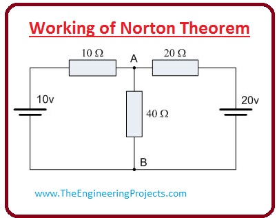
- As we have discussed different steps to apply the Norton theorem. Now we apply these steps practically on a given circuit.
- In the specified figure, we construct a circuit which has three resistances and two voltage sources.
- To apply the Norton theorem, first of all, remove the centered forty-ohm resistor and join the terminals A and B then we get circuit shown in the figure, represented by A.
- When we join two points A and B, then 2 resistances become parallel to each other then we can find the current passing through this 2 resistance.
I1=10v/10ohm = 1A,
I2 =20v/20ohm =1A
- The value of the short current is the sum of these two currents.
I (Short-Circuit) =I1 + I2= 2A
- Now if we remove the voltage sources from the circuit and connect open points with each other and also open the connection among the point A and point B.
- Now the 2 resistances are efficiently linked with each other in parallel.
- The values of interior resistance (Rs) can be found by the sum of resistance at point A and B, the circuitry for this procedure is shown in the figure and represented by B.
RT =(R1 x R2)/(R1+R2) =6.67 ohm
- After finding the value of the equivalent resistor (Rs) and short circuit current (Is), we make a Norton corresponding circuit. Which is represented in the picture by C.
- Now we have made Norton equivalent circuit, but we have to resolve circuit for the forty-ohm resistance which is connected across the point A and point B. this circuitry is signified in the figure by D.
- We can see in diagram (D) that the two resistors (Rs) and (RL) are now connected in parallel so we find the values of total resistance Rt.
Rt= (R1 x R2)/(R1+R2) = 5.72 ohm
- The value of the voltage at point A and B with load resistance is found by the formula.
VA-B = I x R =2 x 5.72=11.44V
- The value of current across load resistance is;
I= V/R=11.44/ 40 =0.29A
Limitations of Norton’s Theorem
- This formula is appropriate for the linear modules like resistors.
- It’s not for such modules which are not linear like diodes, the transistor.
- It also not operate for such circuitries which has magnetic locking.
- It also not work for such circuitries which has loaded in parallel with dependent supplies.
It is the detailed article on the Norton Theorem if you have any question about it ask in comments. Thanks for reading. Take care until the next tutorial.
What is Thevenin’s Theorem
Hello friends, I hope you all are doing great. In today’s tutorial, we will discuss
What is Thevenin’s Theorem. There are a lot of techniques to solve complicated circuitries such as KCL and KVL. In-circuit terminology, this theorem permits any single port (The port is a pair of points which link any circuitry with the other circuits) system to transform into such circuitry which has one resistor and a single source. This method also works for the alternating current (AC) circuitries which have resistive and reactance impedances. It displays that this formula is work for (alternating current) AC circuits if these circuits have impedances instead of resistance.
This theorem was created by the French Engineer, who was specialized in telegraph engineering. In 1882 when Kerchoif’s Laws were very famous to solve circuits but these laws were difficult to implement for complex circuits. To solve complex circuits Thevenin gave his famous law which makes complicated circuits very easy to solve. In today’s post, we will have a look at its equation, example circuits, working, and applications. So, let’s get started with a
What is Thevenin’s Theorem.
What is Thevenin’s Theorem
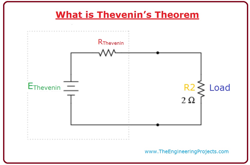
- Thevenin Theorem stated that the circuitry which has many resistors and voltage sources can be transformed into such circuitry which has one resistance and single source.
- To see how this rule works we solve a circuitry.
- In the given diagram, you can see that there is 20 volts voltage source and 15-ohm load resistance which is represented by R3.
- To apply Thevenin theorem to this circuit, first of all, we find VTH which is open circuit voltage for this we will eliminate the load resistor from the circuit. After removing R3 we get the resultant circuit which is represented by B in the diagram.
- Remove all voltage sources from the circuit and put their internal resistances value in the circuit.
- Then calculate the equivalent resistance which is also known as the Thevenin resistance, the resultant circuit is shown in the given diagram as C.
- After this make Thevenin equivalent circuitry which has source and Thevenin resistance then add load resistance to the circuitry to find the voltage across it. Thevenin equivalent circuit is denoted as D in a given diagram.
Why we use Thevenin Theorem?
- The most complex systems of circuits have some non-variable components and some have variable.
- The suitable example for this is our house wiring circuitry which is joined with the different loading devices like motors, fans or some lighting.
- If some time in special cases we want to find current and voltage values at every component of house wiring. It will take time and will be very difficult to find the electrical parameters of every element.
- To reduce these difficult calculations, a resultant circuitry of house wiring is created so that we can easily find the parameters and analysis of circuitry become easy.
- This equivalent circuitry which we make to reduce our calculation easy is called Thevenin equivalent circuitry.
Working of Thevenin’s Theorem
- To observe the practical implementation of Thevenin theorem, we will discuss its working by a given example.
- We create circuitry to calculate the value of current (I) moving in the circuitry.
- To implement Thevenin theorem we have to monitor these 3 steps.
- First of all, calculate the value of resister by eliminating EMF sources and load resistance.
- Then find the Thevenin voltage (V) after inserting the voltage (V) source in circuitry.
- Then already find resistance and voltage values which are Thevenin voltage and resistor use to find current passing through the load.
- Now we apply these steps practically on a circuit.
Step 1:
- In given circuit diagram we can see that forty-ohm resistance, which linked with the points A and D eliminate this resistance and all voltage sources in the circuit.
- After this, we will develop a circuitry which has only 2 resistances in the circuit.
- Now we calculate the value of Thevenin resistance (R), R1 and R2 are parallel to each other.
Rt = (R1 x R2)/(R1 + R2) = (20 x 10)/(20+10) = 6.67 ohm
Step 2:
- In this step we will add, removed voltage sources to find the value of thevenin voltage.
- In the given diagram, we can use ohm law to find the value of the current flowing in this circuitry.
I= V/R = (20v-10v)/(20ohm + 10 ohm) = 0.33A
- Now we find the value of voltage.
VAB = 20 - (20 ohm x 0.33A) = 13.33 V
VAB = 10 + (10 ohm x 0.33A) = 13.33 V
Step 3:
- Now we have our Thevenin Resistance and Voltage we can put our Thevenin equivalent circuit together with our original load resistor as shown below.
- As we have found resistance and voltage values, now we find the value of current the circuit for the third step is shown in the given diagram.
- We use ohm’s law to measure the value of the current.
I= V/R = 13.33V/(6.67 +40) = 0.286A
Limitations of Thevenin Theorem
- These are some limitations of Thevenin Theorem, you must keep in mind while working on the different circuitries.
- This theorem is only appropriate for such circuitry which has linear elements like a resistor, capacitor, etc. It will not work for such circuitries which has the diodes, transistors these are not linear components.
- It also not work for the uni-lateral systems.
- It also not work for such circuit which has magnetic linking among the load and the circuitry which has to convert into the Thevenin circuitry.
Applications of Thevenin's Theorem
- These are some applications of Thevenin Theorem.
- This rule is applied to such circuitries in which load resistance varies, after some time it necessary to measure the value of resistance, Thevenin theorem is best for this circuitry to find the value of current and voltage.
It is the detailed article on the Thevenin Theorem. If you have any question about it ask in comments. Thanks for reading. Take care until the next tutorial.
What is Ohm's Law
Hello friends, I hope you all are doing great. In today's tutorial, we will discuss
What is Ohm's Law. In 1781 an English scientist and philosopher Henry Cavendish was doing an experiment on the tubes which were prepared by the brittle material like glass to measure their radius (r) and length, tubes were full of salty solutions. During this test, he computes the current which he sensed as he accomplished the circuitry with his body. By this observation, he referred that the current is directly proportional to the voltage. He didn’t share his finding to other people and his findings remained unknown till 1879 then Maxwell shared them with other scientists. To practically see the working of ohm's law, you should try our online
Ohm's Law Calculator.
In 1814 Francis Ronald said that findings of Cavendish are not accurate but in the presence of certain conditions like temperature, pressure. After Frances Ronald Ohm’s work on Cavendish theory in 1825 and gave his findings in 1827. In today’s post, we will have a look at its working, introduction, circuit, and applications. So let’s get started with
what is Ohm's Law.
What is Ohm's Law
- Ohm's law says that the current passing through any conductor among 2 points is directly proportionate to the voltage across 2 points of the conductor if physical parameters like temperature, pressure, etc of conductor remain same.
- Its mathematical expression is.
V a I
V= IR
- In this equation (I) is the current passing through the conductor its units is amper (A), V is the voltage which is provided to conductor its unit is volts (V) and R is the resistance of the conductor it does not depend on the current of conductor the value of resistance depends on the physical parameters like temperature, pressure, etc.
- We can also define resistance as if one ampere of current is passing through any conductor when one-volt voltage is applied to it then it has a one-ohm resistance.
R (Ohm)= V (Volts) / I (amperes)
- The diagram on the right side explains Ohm's Law.
- This is an experimental law which describes the conductivity of materials over the current passing through them.
- There are numerous substances which do not follow Ohm’s findings is known as non-ohmic like semiconductor devices diodes, transistors, and bulb filament.
- A component which follows ohm's Law is known as the ohmic like Aluminium, Copper, etc.
- Such conductor which follows Ohm law its graph remains straight line and which do not follow Ohms law its graph is not a straight line.
Parameters of Ohm's Law
- Ther are three main parameters at which ohm's law depends first one is voltage, second is current, third is resistance. Now we discuss them with detailed and relate them.
Voltage:
- Voltage is the force which exerts by the source in electrical circuitry on the electrons to move in the circuit.
Current:
- It is the rate of movement of charges, it's unit is ampere. It denoted as I.
Resistance:
- It is the capability of the substance to oppose current which passing through that conductor. It designated as R and its unit is ohm.
What are the Ohmic and Non-ohmic Conductors
Ohmic Conductor
- Those elements which follow ohms rule are recognized as the ohmic. These modules have a similar value of resistance (R) when we alter the value of current and voltage.
- A graphical demonstration is revealed in a given figure you can see that their graph is a straight line.
- The example of such units is metals like aluminum (Al), copper (CU), etc.
Non-ohmic Conductor
- Those modules which do not follow the ohms rule is recognized as non-ohmic. In these constituents, the value of resistance does not remain the same when we alter the applied voltage.
- The examples of these modules are semiconductor diodes, transistor, and filament of the bulb.
- You can see the graph of non-ohmic devices in a figure that the graph is not a straight line like the ohmic devices because the resistance of these components is not the constant.
Analyze Ohm's Law with the Given Circuit
- In given circuit diagram there is a very simple circuit which consists of one battery and load. Current is flowing through the circuit.
- If we know any two values of either current, resistance offered by load or voltage then we can easily apply ohm's law to find the third value.
- First of all, we calculate the value of current passing through the circuit which is shown on the left side in the diagram, the values of battery is 20 V and resistance is 5 ohm then according to Ohm's law the current is.
I=V/R = 20/5= 4
- Now we calculate the value of voltage by applying the Ohm's Law on right side circuitry.
V=IR = 4 x 5 = 20
Limitations of Ohm's Law
- These are some limits of ohms' law which are described below.
- It is not useable for individual or unilateral circuits. Such circuitries allows current to move in one direction only.
- These circuitries comprises semiconductor devices like diodes and transistor which allows current to move in one direction.
- This law is also not applicable to such components which are not linear, non-linear components are such which in which current variations are not the same to voltage changes. Such components are thyristor.
Applications of Ohm's Law
- Ohm's law is very easy to understand and implement for calculations of current-voltage, or resistance in any circuit.
- The practical uses of ohms law we do to control the speed of fan at our houses. We control speed by the regulator, basically, we vary resistance through the regulator.
- An electrical heater which we use in winter follows ohms law the heat which it produces can be found by using ohms law.
- Electrical kettles also work on the ohm law it has high values resistance which produces heat when the current passing through it we can find the value of this heat by finding current and resistance of kettle.
- The electronic components like laptops, computer, and mobile also follow ohm law because they work on dc so during their designing the values of resistances measured by ohms law.
- Fuse also works on the ohms law its resistance values measure by the ohms law.
So it was all about ohm's Law if you have any question about asking in comments. Take care until the next tutorial.
What is KCL (Kirchhoff's Current Law)
Hello friends, I hope you all are doing great. In today’s tutorial, we will discuss
What is KCL ( Kirchhoff's Current Law ). KCL (Kirchhoff's Current Law) is the fundamental rule of electric circuitries. In 1845 a German physicist Gustav Robert Kirchhoff presented two essentials rules to explain different circuitries. Ist law is KVL (Kirchhoff's Voltage Law) and 2nd is KCL (Kirchhoff's Current Law). These rules further defined the working of Georg Ohm, who gave Ohm’s Law and lead the work of James Maxwell who gave Maxwell equation.
Both of these rules also work for a time (t) and frequency (f) measurements. In certain cases when the frequency of a signal is higher these laws work for the alternating current circuitries. In today’s post, we will have a look at its overview, working, example circuits and other parameters. So, let’s get started with a
What is KCL (Kirchhoff's Current Law ).
What is KCL ( Kirchhoff's Current Law )
- KCL ( Kirchhoff's Current Law ) is also known as the ist rule of Kirchhoff. This law explains that current coming toward a point of the circuit is equal to the current moving away from that point in a circuitry.
?I = 0
- KCL is also named as conservation of charge because the current at the common point in circuitry remains reserve which means there is no loss of current at a point.
- Kirchhoff's Current Law is used to measure current in the different branches of any circuitry. How it finds current for this we explain a simple circuit.
- In given circuitry you can see that the there are six branches of circuitry which are connected with the common point, this common point is also known as a node.
- In this circuitry, the direction of current in these six branches is denoted by a, b, c, d, e, and f.
- As we discussed earlier KCL says that current coming toward a point is taken positive and moving away negative. You can see in the circuit that the currents (a, b, c, d) are coming toward the common point so these will be taken positive and current (e, f) will be negative as they are moving away from the point.
- If we apply KCL to this circuit then the resultant equation will be.
a+b+c+d=e+f
Working of KCL( Kirchhoff's Current Law )
- Now we discuss how this law works for this we explain the given below simple circuit. Let's discuss it.
- In this circuit we can see that there is a node which has four wires connected with it, the current is passing through every wire.
- If we apply the KCL to the circuit then the equation of this circuit is
(I1)+(I2)–(I3)–(I4)=0
- This equation can also write to describe the inward current to the node and moving away from the current for the node.
(I1)+(I2)=(I3)+(I4)
- This equation shows that (I1) and (I2) is coming toward the node and the (I3) and (I4) moving away from the node.
- To the easy understanding of this law, we relate this given circuit with the liquid circuitry.
- Let's suppose we have a pipe in which liquid is moving with the rate of flow (Q1).
- If we divide this pipe into 3 smaller tubes, then the rate of flow of coming liquid will be equal to the liquid moving away from the center point. To further understanding lets see a diagram of this liquid circuitry which is similar to the KCL.
(Q1) = (Q2) + (Q3) + (Q4)
Nodal Analysis
- This method used KCL to find the value of the voltage at the node and then calculate the values of current and voltage at any component of the circuit.
- There are some steps you should follow to apply this rule which described below.
- To apply this rule, first of all, you should find the no of nodes in a circuit and reference node.
- Then allocate current and its path to every discrete division (branch) of the nodes in the circuit.
- Apply KCL to every node of the circuit.
- Then make equations and resolve them to find the values of current (I) and voltage (V).
- Then find the values of current (I) and voltage (V) at every component of circuitry.
Example of Nodal Analysis
Now we discuss how nodal analysis works practically and have a relation with the KCL.
- The values of some elements which we know are given here.
- Current Source (Ix)= (5 Amperes)
- Current Source (Iy)= (10 Amerces)
- Resistance (R1) = (4 Ohms)
- Resistance (R2) = (2 Ohms)
- Resistance (R3) = (6 Ohms)
- First of all, we find the reference node in this circuitry, we consider V0 as a reference node because it is joined with the ground terminal.
- As we know at ground potential is 0 so this will make our calculation simple.
- You can see there are three nodes in this node first one (V1), 2nd is (V2) and third is V0 which is our reference node.
- Now we use KCL on a node (V1) and node (V2) to find their equations.
- The equation for the first node will be.
(Ix ) = (I1 + I2)
(Iy)= (I3 – I1)
- Now we put values of known elements of circuitry.
(5 A) = (I1 + I2) – (A)
(10 A) = (I3 – I1)- (B)
- You can see from the figure that there are three unknown currents is moving in this circuitry (I1, I2, I3) we use ohm’s law to find their equations.
(I1)= (V1-V2)/R2
(I2)= (V1-0)/ R2
(I3)= (V2-0)R3
- Now we put these current values in equation A and B.
- First we put these values in equation A.
5 = (V1-V2)/R2 + (V1)/ R2
5= (V1-V2)/4 + (V1)/ 2
5 = (V1 - V2 +2V1)/(4)
20 =3V1 – V2 - (C)
- Now we will put the values of (I1,I2, I3) in equation B and make resultant equation.
10= (V1)/ R3 - (V1-V2)/R1
10=(V1)/ 6 - (V1-V2)/4
10= (2v1-3V1 + 3V2)/12
120= -V1 + 3V2 – (D)
- Solving equations C and D we have the values of V1 and V2.
V1 = 22.5v
V2 = 47.5V
- Now we use these values and find the (I1,I2, I3).
(I1)= (22.5- 47.5V)/4
(I1)= (-6.25A)
(I2)= (V1)/ R2
(I2)= (22.5)/ 2
(I2)=11.5
(I3)= (V2)R3
(I3)= (47.5)/6
(I3)= 7.91 A
Applications of KCL Law
- These are some applications of this law.
- KCL is used to find the different electrical parameter like current, voltage and resistance in different circuits but it mostly used in complex circuits to find electrical parameters.
It was a detailed article on KCL law I tried my best to write in a simple way. If you have any question about it ask in comments. I will guide you comprehensively. Thanks for reading. Take care until the next tutorial.
What is KVL ( Kirchhoff's Voltage Law )
Hello friends, I hope you all are doing great. In today’s tutorial, we will have a look at
What is KVL ( Kirchhoff’s Voltage Law). KVL is an elementary law of electrical circuitry. In 1845, a German physicist
Gustav Robert Kirchhoff gave two basic laws to solve electronic circuits. First one is KVL ( Kirchhoff’s Voltage Law ) and the second one is
KCL ( Kirchhoff’s Current Law ). These Kirchhoff's laws are successors of
Ohm’s Law which was given by George Ohm and followed by Maxwell equation which was given by James Maxwell.
Both of these laws playing a very important role in solving different circuits in engineering projects. These rules are also useful for frequency and time calculations. Kirchhoff’s laws are not only applicable to DC circuitry, but also works for the AC circuits, when the electromagnetic radiation has large frequency values.
In simple words, KVL says that the sum of voltages in an enclosed loop circuit is always equal to zero. By using this law we can easily find different parameters of a circuit like resistance, current or voltage quite easily. In today’s post, we will have a look at its introduction, working, applications and other parameters. So, let’s get started with
What is KVL ( Kirchhoff’s Voltage Law ).
What is KVL ( Kirchhoff’s Voltage Law )
- KVL ( Kirchhoff’s Voltage Law ), also known as the second rule of Kirchhoff’s, explains that the sum of voltages in an enclosed circuitry is always equal to 0.
- KVL applied for voltage measurement in circuits. To explain it we discuss given circuitry.
- As you can see in a given circuit that the single voltage source is linked with the passive elements (the electric element which does not produce power like a resistor), which have (b,c,d,e,f) voltage about them.
- As all these elements are connected in series so there voltages values will be added.
- If we apply KVL (Kirchhoff’s voltage law) which says voltage around the passive (the electric element which does not produce power, like a resistor) element in circuitry always equivalent and reverse to source voltage.
- Therefore, the summation of the voltage changes across all the elements in circuitry is always equated to 0.
a+b+c+d+e+f=0
What is Mesh Analysis
- It is the method to helps us to find the current and voltage in any close-loop working with the KVL, by this analysis we can find values of current and voltage across any component of the loop on the circuit.
- There are three steps to apply this mesh analysis. Which described here.
- Allocate discrete current values to every enclosed circle of the network.
- After that Apply Kirchoff voltage law about every enclosed circle of the system.
- And resolve the resultant concurrent linear equations to find the value of current in the ring.
Example of Mesh Analysis
Now we practically discuss the Mesh Analysis by the given example.
- Let's suppose that we have a given circuit diagram which has two loops and we have to apply mesh rule on this circuit.
- The values of the elements of this circuit which we know are given below.
- (R1)= (5 ohms)
- (R2) = (6 Ohm)
- (R3)= (10 ohms)
- (V1) = (12 volts)
- (V2)= (8 volts)
- To apply mesh rule on this circuit, first of all, we recognize the direction of the current flowing in these two loops.
- In the first loop which is (ABEF) the direction of current is clock-wise and it is represented as (I1).
- In the second loop which is (BCDE) the direction of current (I2) is also clockwise.
- Now applying kVl to write the equation for both of these two loops.
(V1)= (R1I1)+ R3(I1 - I2)
- This equation can also be written as
(V1)= (R1 +R3)I1-R3I2 – (A)
- Now if we apply KVL on loop 2 then we have this equation.
(V2) = (R2I2) + (R3)(I2-I1)
- It can also be written as
(V2) = (R2+R3)I2 –(R3I1) – (B)
- Now we will put the values of given parameters of circuit and find the value of the unknown parameter.
(12) = (5+10)(I1)- (10)I2
12= (15I1)- (10I2) –(C)
- When we put value in equation B it will become
(8)= (6+10)(I2)- (10)(I1)
8=16 (I2)-10(I1) –(D)
- By solving equation C and D we have.
I1= 1.94 A
I2=1.7 A
Example of KVL ( Kirchhoff’s Voltage Law )
- In the given diagram, a circuit is drawn at which we have to apply KVL.
- In this circuit, there are three loops which are labeled in the circuit by no 1, 2, 3.
- We will apply KVL on these three loops one by one and will get correspondent equations.
- When we apply KVL to the first loop we get this equation.
V1= (I1 x R1) + R3(I1+I2)
10= (I1 x10) + 40(I1+I2)
10= 50 I1 + 40 I2
- After applying KVL on the first loop we now apply it on the second loop then we get an equation for this loop.
V2= (I2 x R2) + R3(I1+I2)
20= (I2 x 20) + 40(I1+I2)
20 = 40 I1+ 60I2
- After findng equations for loop first and second now we find the equation for the third loop.
V1-V2 = (I1 x R1) – (I2 x R2)
(10-20) = (10I1) – (20I2)
- By solving equations of loop one and second we get the value of (I1) and (I2) which are mention below.
I1= -0.143 A
I2= +0.429 A
- By using the value of I1 and I2 now we find the value of current I3.
(I3 = I1 + I2)
- Putting the value of I1 and I2 we get current at resistance (R3).
I3 = -0.143 + 0.429 = 0.286 A
- I3 is the current which is passing through the resistance (R3), we can also find the value of voltage across this resistance by using I3.
V3= (0.286 x 40) = 11.44 V
Applications of KVL Law
- These are some important applications of KVL law.
- Kirchhoff’s laws are used to measure the unknown standards such as current (I), Voltage (V), also the direction of moving current in the circuit.
- This rule is applicable to every circuit but it is very fruitful to solve complicated circuitries.
- This law also helps us to observe the transferal of power in the circuit.
This article was about KVL law, I tried my best to explain to you in the simplest way if you have any question about it ask in comments. I will solve your problems and will guide you comprehensively. Thanks for reading. Take care until the next tutorial.
Top Modern Construction Materials Boosting the Sector’s Growth
Traditional concrete can develop cracks through recurring freeze-thaw cycles over time. Cracks expand as it freezes, potentially letting water seep in further pulling it apart. Just as concrete deteriorates, steel structures do too due to inevitable corrosion. The rusted steel eventually wears the entire structure, threatening a crash if not inspected by a safety engineer. Innovations in building materials are rapidly disarming hazards posed by old materials—a British steel company patented a new form of colour-coated steel, galvanized steel, being used as additional protection against adverse environmental factors. Read more
here.
Researchers have pondered whether materials could be made as such to bounce back from harsh conditions and vulnerabilities. How about self-healing concrete? Or recycled waste used in insulation works? The construction industry can shave off billions in reworks and repairs of faulty building work while cutting down greenhouse gas emissions. Day by day, the industry is marching toward a progressive era of reusable construction materials and nullifying options that serve no one.
Modern construction materials breed modern construction methods. They will bring more strength, safety, and cost-efficiency to structures of tomorrow that’ll enhance their longevity and usability.
Here are five new materials boosting the construction sector’s growth.
Self-Healing Concrete
One of the first scientists to create self-healing concrete, Dr. Schlangen of Delft University has demonstrated that the material can be joined back if its half-sliced pieces are put together and heated in a microwave. This technology innovation can save companies $90 million annually.
Self-healing concrete will help build structures that last—from small shops to skyline-expanding high-rises. These structures will carry minimal repairs and would facilitate easier maintenance. Project owners want to ensure their build not only stays functional in its lifetime but offers incremental benefits to end users, for this to become a widespread reality, builders will have to consider self-healing concrete more aggressively since construction costs are higher with regular concrete that also poses durability threats as the climate worsens.
Using the right materials is only half the battle, making decisive shifts on jobsite is the other half. New building materials will need the consensus of all stakeholders down to the last subcontractor on the project. Without it, flaws in construction processes emerge faster than realized which leads to reworks. Contractors are pressed to extend timelines lest quality suffers and to ensure they’re on track, they use punch lists.
Get more info on how best can punch lists be optimized for maximum results.
Eco-Friendly Bricks
Studying the effect of built environments on occupants, safety and environment specialists are closer to home with their understanding of indoor air quality. Many indoor air cleansing solutions have been introduced but none as efficient to recognize as a permanent fix to continuing air contamination affecting respiratory health. With traditional solutions, more carbon is emitted into the atmosphere, deteriorating outdoor air as well.
Thanks to Cal Poly School of Architecture’s assistant professor, Carmen Trudell, who invented a passive air-cleaning system that puts bricks used on the building’s exterior to filter out toxins and pollutants in the air as it lives inside the space. The air will get funnelled into an internal cyclone filtration section separating heavy elements and dropping them down a hopper at the wall’s base. This pulls clean air into the building with maintenance being only to the extent of removing and emptying the hopper periodically.
Energy-Efficient Cement
Building energy-efficient structures will never go out of style—and, the industry is evolving at breakneck speed to accommodate environmental costs into the build process. One such endeavour is to make cement perform as an energy-saving agent through the process of polycondensation of raw materials including industrial waste, silica, water, alkali, and river sand. Conducted at room temperature, the process uses less energy.
As is popularly echoed, the future is in part influenced by the past—so when researchers look to
eco-friendly new construction materials, they need to grasp what didn’t work with old alternatives. A surge in interest in Roman concrete has thus been stumbled upon as it embodies less energy than the popularly used Portland cement while being much more durable beyond the traditional lifespan of modern architecture. Unexpected weather incidents endanger our infrastructure and buildings for which stronger and energy-efficient materials are important to ensure projects endure the coming times.
Laminated Timber
Widely used 50 years ago, timber’s use is declining today. But cutting-edge engineering has made timber stronger and durable to support heavy structures.
Researchers have developed laminated timber, also called glulam, to create a more water-resistant and durable replacement for wood. This has made timber highly cost-efficient with its current use in projects saving wood usage. Wooden structures absorb a ton of energy and this development couldn’t have been more opportune. Substituting wood with laminated timber would cut down about 3,000 tons of carbon emissions gradually increasing as more builders adopt it.
Reprocessed Scrap Material
Turns out the trash isn’t trash, after all, recycling can make the worst material beneficial. Builders have pioneered the use of recycled scrap such as cardboard, plastics, leftover metal to build structures registering minimal carbon footprints.
When cardboard’s recycled, it’s used for high-quality cellulose insulation that outperforms traditional insulation. Replacing dry processes that generated incalculable filth and dust, cellulose insulation renders air clean. Another scrap material recycled is plastic—from small bags to large containers, recycled plastic can last a few times that cuts new plastic production by a significant number. An unprecedented innovation, PET (polyethylene terephthalate) carpets have given a new lease of life to plastics, turning them into fibrous soft reusable carpets with no expiry date that can be used in insulation.
Closing Comments
Making materials sustainable isn’t a fad. It’s here to stay. It has been having a big impact on construction in multiple ways beyond direct construction activities. It has helped construction companies expand engineering teams for R&D and safety implementation as these new building materials require periodic upgrades like any new technology.
As the industry opens up to eco-friendly substitutes, construction projects would gradually substantially reduce harmful environmental effects. Conscientious builders will get in on the fun early on, leverage competitive edge, and win more bids and public goodwill as they seek to improve the economic status of the sector through redefining how materials are made and used.
6 Types of Industrial Robots
Hello friends, I hope you all are doing great. In today's tutorial, we are gonna have a look at
6 Types of Industrial Robots. Industrial and commercial robots make work easier and increase efficiency and accuracy. This of course means more profits for the industries that employ these robots. The modern robots are nothing like the robots of yesteryear. These older robots were bulky and took too long to program. Today’s robots are collaborative robots (cobots), designed to work alongside humans in a shared work area.
These robots are easily programmed, are flexible and they are a much-needed supplement to skilled workers.
Cobots have highly sophisticated sensors that allow them to work near humans. Once they sense a human presence, they either slow down or shut down accordingly. They are very useful in situations where high accuracy is needed, or jobs that involve repetitive movement.
There are many types of industrial robots, with the main ones being:
#1. Articulated
The articulated robot design has rotational joints which can be anything between a simple two jointed structure to complex ones with 10 joints that interact, or more. The arms are connected to a base which has a twistable joint. The arm links are connected to each other by rotary joints. Each joint is known as an axis and it provides the robot with an extra degree of freedom to swivel. Industrial robots mostly have about four or six axes.
The articulated
commercial robots are powered by different means, which includes, but is not limited to electric motors. Most robots used in industries worldwide are articulated robots. Articulated robots can be utilized in material handling and removal among others.
#2. Cartesian
These also go by the name gantry or rectilinear robots. They consist of three linear joints that make use of X, Y and Z or
Cartesian coordinate system. These robots have a wrist attached, which allows rotational movement. These three joints in the form of a prism give a linear movement on the axis.
#3. Cylindrical
This type of robot has at the very least, a single rotary joint at its base, and one slider which connects the joints. Rotational motion is used by the rotary joint along the axis joint, and the slider joint moves in a straight motion. Cylindrical robots work within a cylindrical work envelope.
#4. Polar
These are
also known as spherical robots. Their arms are joined to the base with a joint that twists, and two rotary joints combined with a single linear joint. The axes make a polar co-ordinate and thereby create a spherical-like work envelope.
#5. SCARA
The SCARA acronym means Selective Compliance Articulated Robot Arm or Selective Compliance Assembly Robot Arm. This type of robot is normally used in assemblies. This robotic arm is cylindrical in shape and features two joints that are parallel to each other and that give compliance in one chosen plane.
The SCARA is a manipulator that has 4 freedom degrees. It is used to improve repetitiveness and speed in pick and place jobs, or to improve steps in assembly.
#6. Delta
These robots are
spider-like and consist of three arms that join to universal base joints. Delta robots are mostly used in situations where the robot has to pick products in batches and put them in a container or a pattern. Delta robots have added vision capabilities that allow them to distinguish between colors, sizes and shapes. They then pick and place the objects based on a pattern that is pre-programmed.
By design, the Delta robots move at very high speeds and carry out repetitive tasks with speed and consistency. The robots remove the issue of employee fatigue, caused by repetitive movements. They also remove the problem of injuries caused by repetitive motion caused by reaching overhead, bending or working in uncomfortable positions.
Conclusion
Robots are here to stay, and they will only become more sophisticated in the years to come. 10 years ago, robotics was a whole different ball game from today. A lot of research is being conducted every day and improvements made on existing models. Will we be fully dependent on robots for everything in the next century? Only time will tell.