Introduction to NPN Transistor


What is NPN Transistor?
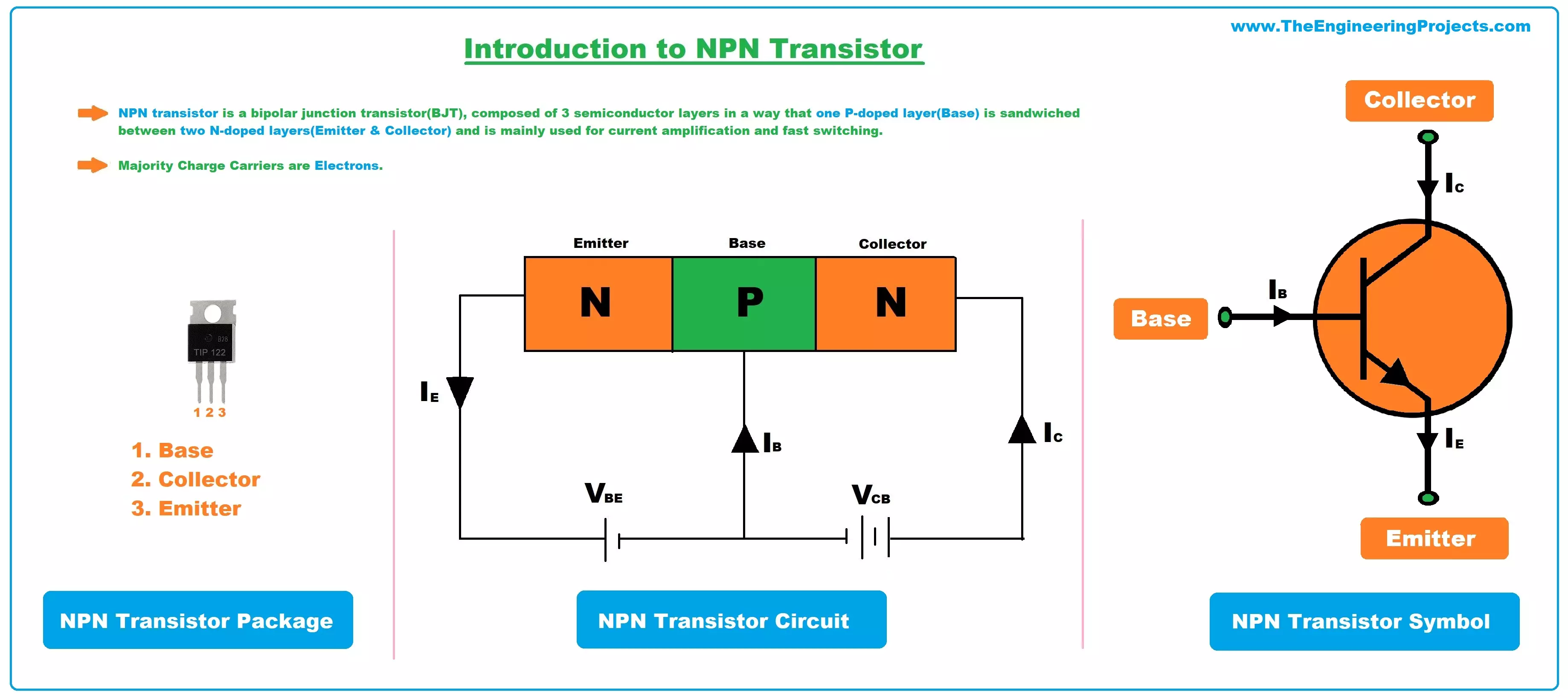
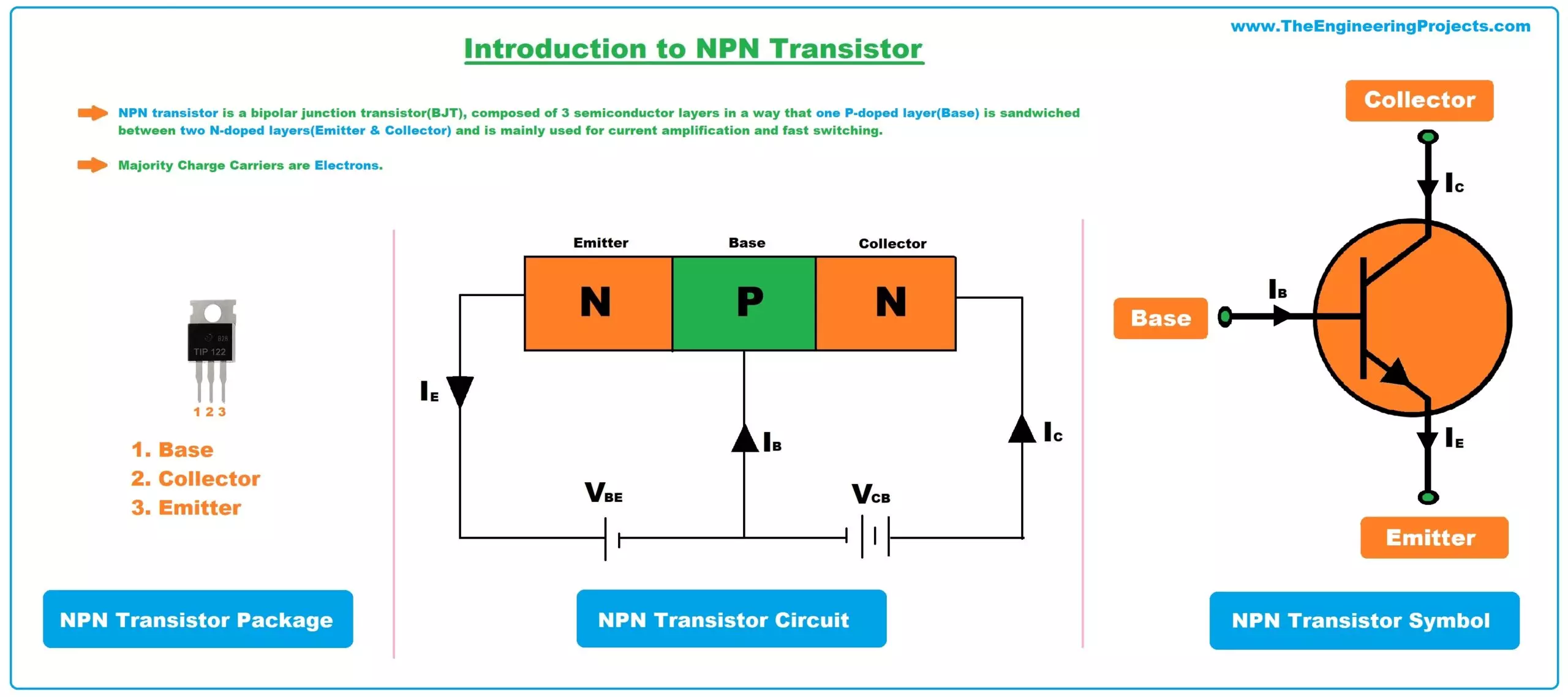
- NPN transistor is a bipolar junction transistor(BJT), composed of 3 semiconductor layers in a way that one P-doped layer(Base) is sandwiched between two N-doped layers(Emitter & Collector) and is mainly used for current amplification and fast switching.
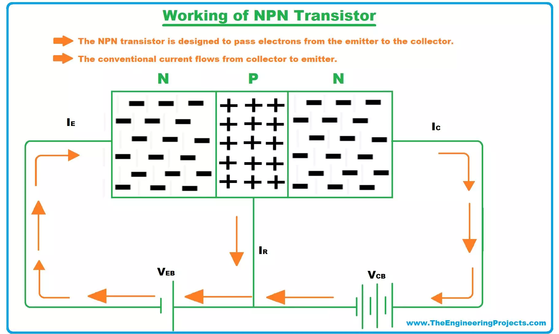
- In NPN transistors, the majority charge carriers are electrons and thus conduction is carried out by the flow of electrons from emitter to collector.
- NPN transistor package comes with three terminals named:
- Emitter.
- Base.
- Collector.
- These terminals are used for external connection with the circuit and a small current at the base terminal is used to control the large current at the collector and emitter side. (We will cover it in detail in the working section)
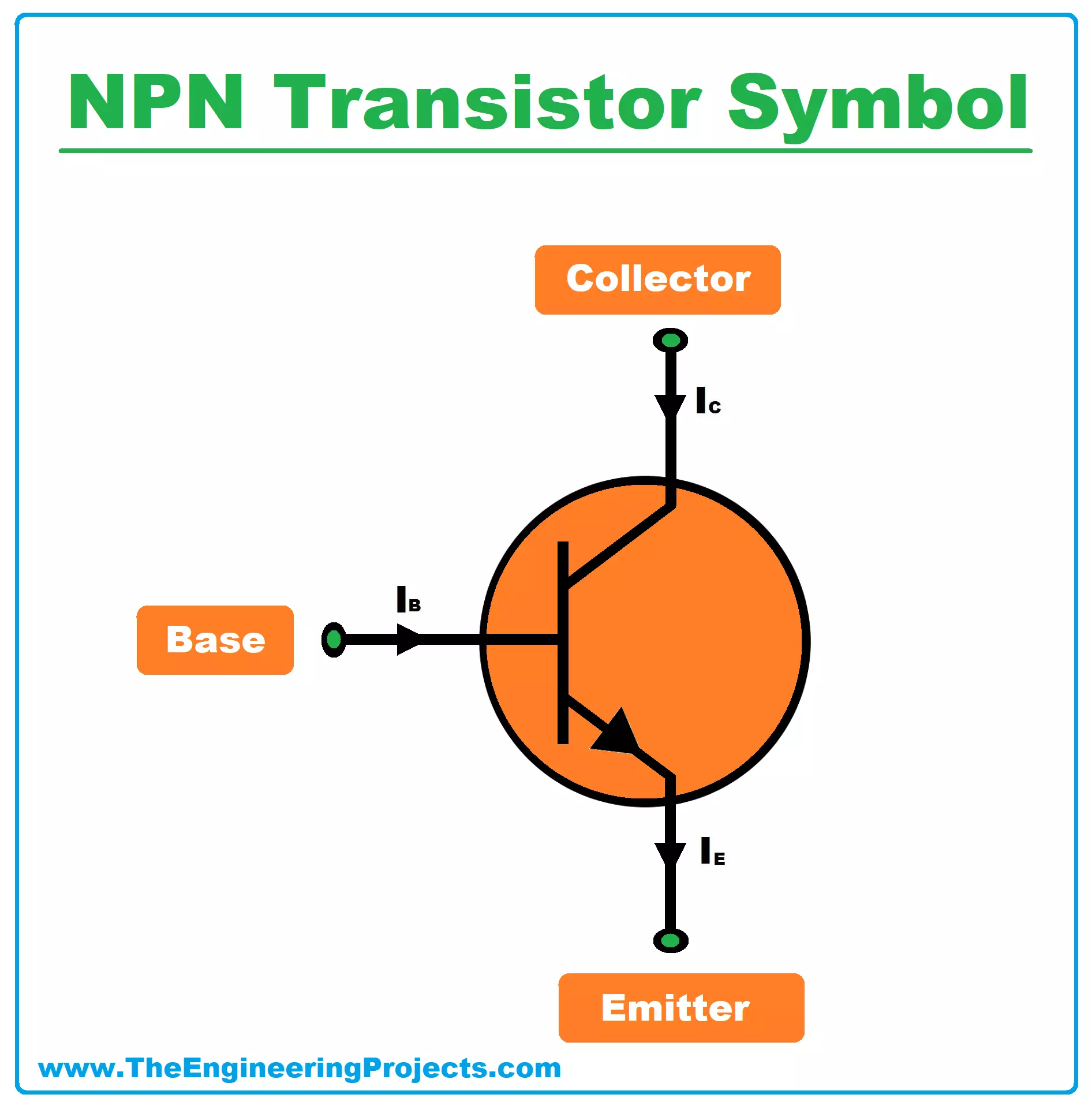
NPN Transistor Symbol
- As we use logos to represent companies, similarly in electronics, specific symbols are used to represent components. These electronic symbols prove helpful in designing circuit diagrams especially block diagrams of electronic models.
- Below figure shows the NPN transistor's Symbol:
Construction of NPN Transistor
- NPN transistor consists of 3 regions, two of them are constructed using N-type semiconductor material while the third one is of P-Type Semiconductor.
- The P-type region is sandwiched between these two N-Type regions.
- So hypothetically, NPN Transistor is constructed by connecting two diodes in opposite directions.
- The equivalent circuit of NPN transistor is shown in the below figure:
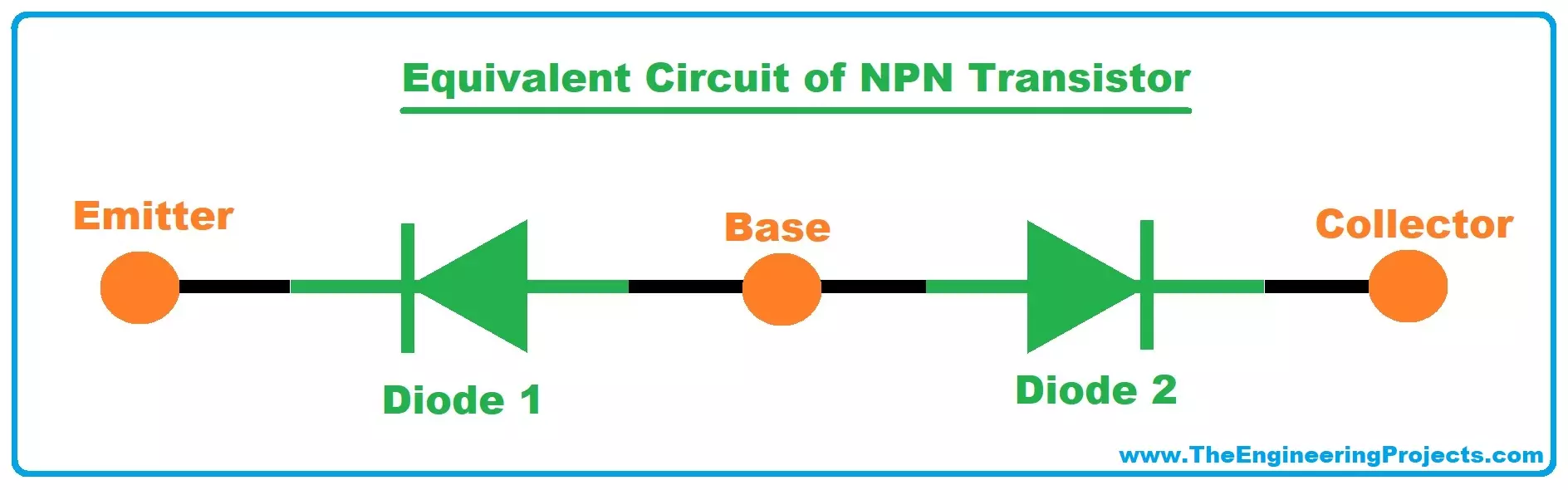
- An NPN transistor has two P-N junctions in it, named as:
- Emitter-Base Junction.
- Collector Base Junction.
Doping Concentration in NPN Transistor
- Impurities are added to Intrinsic(Pure) Semiconductors which increase their conductivity and are called Extrinsic(Doped) Semiconductors.
- In NPN transistors, the Base region is heavily doped, the Emitter is lightly doped while Collector's doping lies in between the Base & Emitter.
- So, in terms of doping concentration from high to low, we have the sequence as follow:
Base > Collector > Emitter
- Moreover, the Base region is constructed using P-type semiconductors, while Emitter & Collector are designed using N-type semiconductors.
How NPN Transistor Works?
- The NPN transistor comes with two junctions, called:
- Emitter-Base Junction.
- Collector-Base Junction.
- The NPN transistor sets in operating condition when an emitter-base junction is forward biased and the collector-base junction is reverse biased and enough current is present at the base terminal. In order to make emitter-base junction forward biased, a positive voltage is applied at the base side and a negative voltage is applied at the emitter side.
- Similarly, in order to make emitter-base junction reverse biased, collector voltage must be kept more positive than base and collector.
Circuit Diagram
Following figure shows the circuit diagram of the NPN transistor.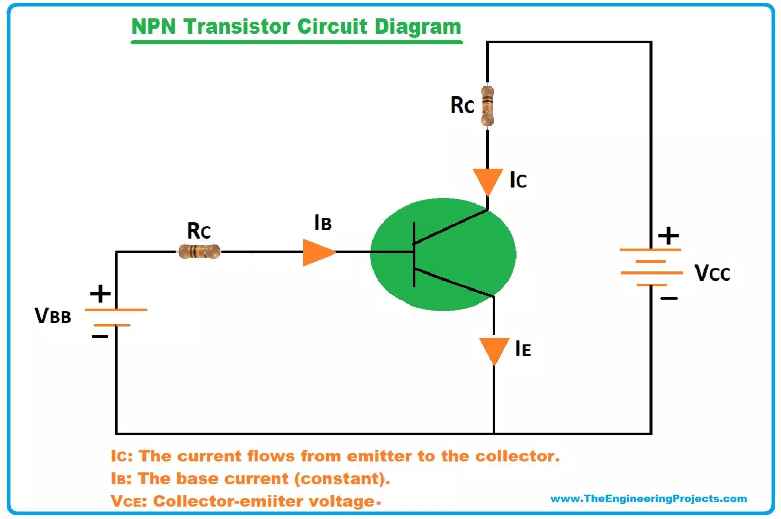
- We can see from the diagram, voltage and resistive loads are applied at the terminals of the transistor.
- A negative voltage is connected to the emitter while a positive voltage is connected to the base terminals.
- The base is more positive with respect to the emitter.
- The resistive load is applied at the base terminal which limits the current produced in this terminal.
- The positive voltage is applied at the collector terminal and load resistance is applied at this terminal that limits the electrons entering at this terminal.
Working
- The base is responsible for initiating transistor action. When a voltage is applied at the base, it gets biased and draws a small current which is then used to control a large current at the collector and emitter side.
- The base action is considered as an ON-OFF valve that generates current when a proper bias voltage is applied at this terminal.
- The small change in the voltage applied at the base terminal shows a large impact on the output terminals. Actually, the base acts as an input and the collector acts as an output in NPN transistor.
- In case of silicon transistor emitter-base junction draws voltage around 0.7 when there is no voltage at the base terminal, in order to initiate the electron action and put the transistor in running condition, the base voltage must be greater than 0.7 voltage in the case of silicon transistor and 0.3 in case of germanium transistor.
- In the N-side of the transistor which represents emitter, the electrons act as the majority charge carriers which are then diffused into the base when a suitable voltage is applied at the base terminal. These electrons act as minority charge carriers when they enter the base terminal, where they join with holes present in the base. Not all electrons join with the holes present at the base terminal. Some of them join with the holes, and the resulting electron-hole pair disappears. Most of the electrons leave the base terminal and then enter the collector region where they again act as a majority charge carriers.
- When a voltage is applied across the base terminal, the base current is given by;
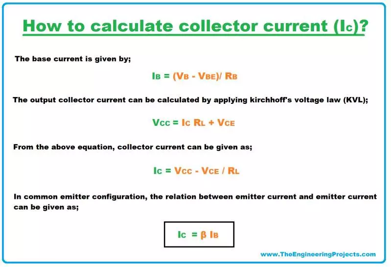
- Collector current is directly related to base current times a constant factor.
- In order to increase the efficiency of the NPN transistor, the base is made very thin and a collector is made thick for two reasons i.e collector can handle more heat and accept more electrons diffused through the base terminal.
Current Gains and Relation between Them
- Current gains play an important role in the amplification process. The common emitter current gain is a ratio between collector current and base current. It is called beta and denoted by ß. It is also known as an amplification factor which defines the amount of current being amplified.
- Beta is a ratio between two currents, so it features no unit. The beta value is always greater than unity and ranges between 20 to 1000 - 20 for high power transistors and 1000 for low power transistors, however, most of the time its value is taken as 50.
- Similarly, a common base current gain is another important factor which is a ratio between collector current and emitter current. It is called alpha and denoted by a. An alpha value ranges between 0.95 and 0.99, however, most of the time its value is taken as unity.
- Following figure shows the relation between two current gains.
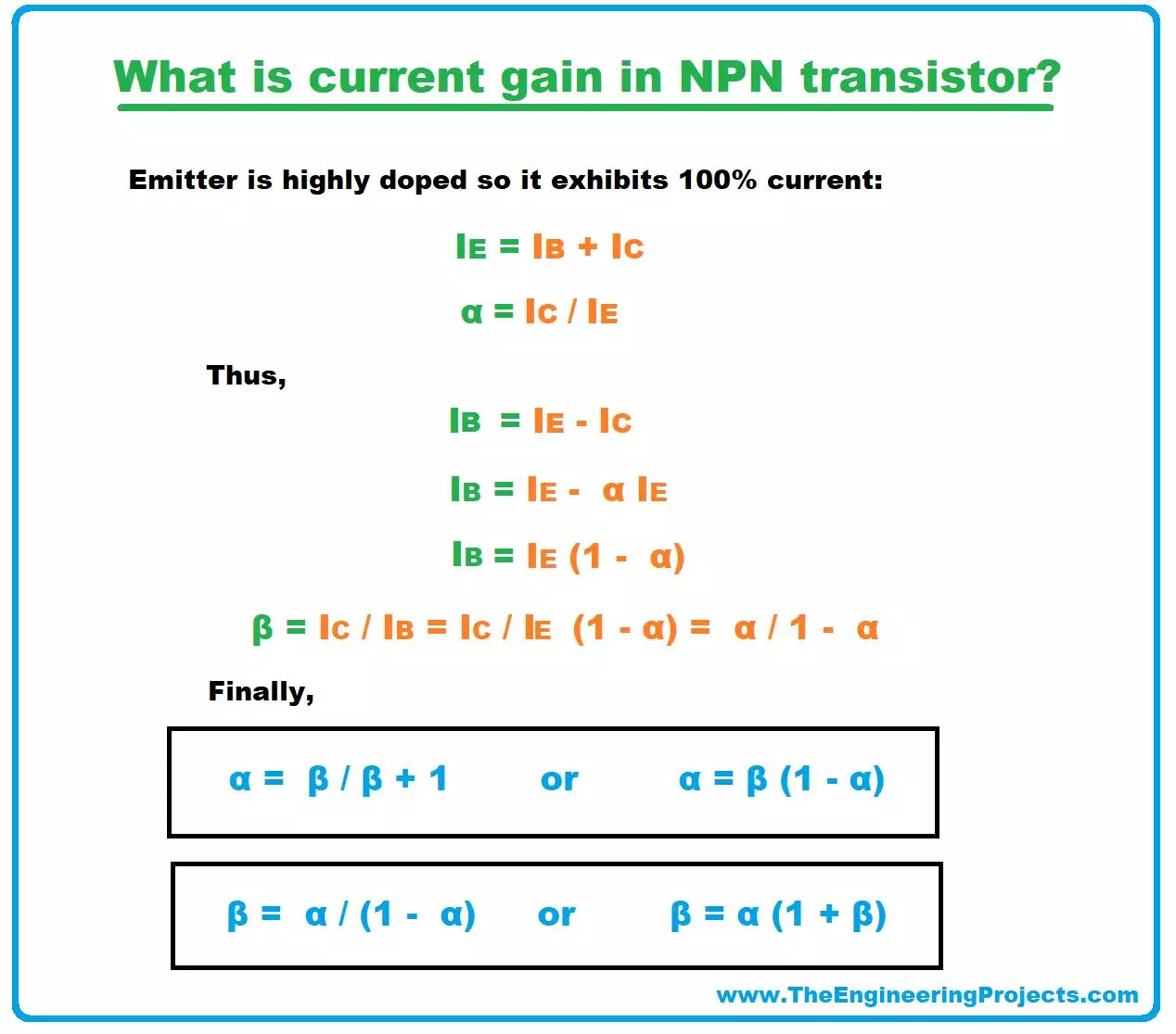
- IF alpha = 0.99 then b = 0.99/0.01 = 99.
- An alpha value cannot exceed from unity, because it is a ratio between collector current and emitter current i.e emitter current always remains greater than collector current because it exhibits 100% current of the transistor and is equal to the sum of collector current and base current.
NPN Transistor Configurations
- This NPN transistor can be configured into three configurations called common emitter configuration, common collector configuration, and common base configuration.
- Common emitter configuration is mostly used for amplification purpose where base acts as an input, collector acts as an output while emitter acts as a common terminal between input and output.
- This common emitter configuration acts always operates in a linear region where small current at the base side is used to control large current at the collector side.
- The common emitter configuration used in the electronic circuits always produces inverted output that is highly affected by the bias voltage and temperature. This configuration is an ideal choice for ampliation circuits because it comes with high input impedance and low output impedance and produces the exact voltage and power gain required for amplification purpose.
- During common emitter configuration, transistor always operates between saturation and cut-off region that helps in amplifying the negative and positive cycles of the input signals. If the base terminal is not biased with the proper voltage, only half of the signal would be amplified.
Output Characteristics Curve of NPN Transistor
Following figure shows the output characteristic curve of the NPN bipolar transistor which is plotted between output collector current and the collector-emitter voltage with varying base current.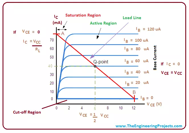
- As described earlier, there will be no output collector current if the applied voltage at the base terminal is zero. When proper bias voltage above 0.7 V, is applied at the base terminal, it gets biased and draws current that controls and effects the output collector current.
- We can see, Vce directly effects the value of output collector current as long as the applied voltage is 1 V. Above that value collector current no longer remains under the influence of Vce value. In that case, the collector current is widely dependent and controlled by the base current. A small change in the base current and bias voltage would produce a large change in the collector current.
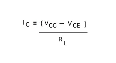
- The load resistor applied at the collector terminal controls the amount of current entering the collector terminals. Keeping in the view of the load resistor and the voltage applied at the collector-emitter terminals, the collector current is given by;
- Straight load line between point A and B falls under active region when an emitter-base junction is forward biased and the transistor conducts where electrons are majority charge carriers.
- The Q point in the graph can be defined by the load line which is actually referred as an operating point of the transistor.
- The output characteristics curve of this NPN transistor is used to describe the collector current when base current and collector voltage is given.
- In order to conduct, collector voltage needs to be more positive than base and emitter.
- It is important to note that, when an emitter-base junction is not forward biased, Ic will be zero, no matter how much voltage is applied at the base terminals. When the emitter-base junction is forward biased and voltage is applied at the base terminal, it draws small current which is then used to control large current at other terminals.
Difference between NPN and PNP Transistors
- Both NPN and PNP transistors are different in terms of electrical construction and layers doping. NPN stands for negative-positive-negative and also known as sourcing device. While PNP stands for positive-negative-positive and also known as sinking device.
- In NPN transistor base is positive as compared to emitter and collector voltage is more positive as compared to both emitter and base. Similarly, in PNP transistor base is negative as compared to emitter and emitter voltage is much larger than collector voltage.
- The voltage polarities and current directions are reversed in both transistors.
- The NPN transistor conducts and initiates transistor action when a positive voltage is applied at the base terminal. The PNP transistor conducts when a negative voltage lower 0.7 V (for silicon) than emitter voltage is applied at the base terminal.
- The NPN transistor uses electrons as majority charge carriers for the conduction while PNP transistor uses holes as majority charge carriers for conduction process.
- In NPN transistor current flows from the collector to emitter while in case of PNP transistor current flows from emitter to collector terminal.
- Both transistors differ in terms of how they are powered on. The NPN transistor powers on when there is enough current present at the base terminal while PNP transistor powers on when there is no current at the base terminal.
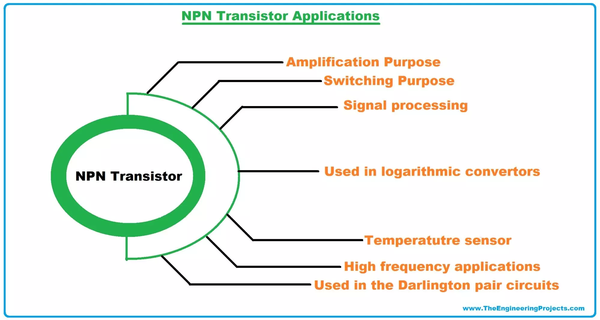
Applications of NPN Transistor
NPN Transistor is the most commonly used type of transistor because of its wide range of applications. A few of NPN transistor applications are as follows:- As NPN transistors are fast switching devices, thus they are used for switching purposes i.e. Pulse Width Modulation.
- NPN transistors are also used as automatic switches in electronics products.
- Because of high current gain, NPN transistors are used for current amplification i.e. small current at input allows heavy current to pass at the output(Ic).
- In embedded computers(i.e. microcontrollers, microprocessors etc.), thousands of transistors are joined together(in SMD form) performing different functions i.e. switching of pins.
Real-Life Applications of NPN Transistor
- Used in logarithmic converters and high-frequency applications.
- Signal processing and radio transmission applications involve NPN transistors.
- Darlington pair circuits make use of this NPN transistor for amplifying signals.
- Used in temperature sensor.
- Push-Pull amplifying circuits, which fall under the category of the classic amplifier circuit, make use of this NPN transistor.
- In small quantities, transistors are used to make logic circuits and in the circuits where amplification is required.
×
![]()