What is the Power Diode

Hello friends, I hope you all are doing great. In today’s tutorial, we will discuss What is the Power Diode. The diode is a commonly used module in electrical and electronic engineering. Almost in every electronic device and engineering project diodes are used. It is a PN junction device that has 2 terminals, anode and cathode. The main function of the diode is to convert the alternating current into the direct current, this feature of the diode is called rectification. When it works on the positive cycle of the alternating current its state named as forward biased when it works on the negative cycle of the ac its operating state known as reverse biased. In 1906 the first diode was manufactured by the crystals of the minerals. Power diode is identical to the other semiconductor diodes but has some differences in structure. Normal diodes are used for smaller amplification and switching circuitries but power diode used in higher amplification circuits. In today's post, we will discuss its structure, applications, circuits, and working principle. So let's get started with a what is the power diode.

What is the Power Diode

  • Power Diodes are such semiconductor devices used in rectifier circuitries to rectify higher value current.
  • This diode has a larger area of PN junction then other diodes, due to this ability is used to rectifier higher value current and voltage, like hundred amperes and thousand kilovolts.
  • In normal diodes, both P and N portion have the equivalent doping level, but in power diodes, one side is highly doped and other is lightly doped.
  • In the given diagram, you can see that there are three regions first one is highly doped (P+) and 2nd is less doped (N-) regions, both of these are joined with the highly doped (N+).
  • The region (N-) is the main factor that makes power diodes useful for higher power circuitries.
  • As (N-) is very less doped, due to this power diode also named as the PIN diode. In (PIN) the I for intrinsic.

Half Wave Rectification of Power Diode

  • Such circuitry that converts the alternating current into the direct current is called rectifier circuit.
  • The rectifier that converts half-wave of the alternating current into the direct current called half-wave rectifier.
Half Wave Rectifier Circuit
  • In the given diagram you can see the circuitry of the half-wave rectifier, that has power diode and resistor (R) as output.
  • You can see from the figure that the anode of the diode is connected with the positive end of the alternating current source through the transformer that used to step down the voltage and cathode is connected with the negative end. It is the forward-biased form of the diode.
  • When the first half waveform of the alternating current passes through the diode, it rectifier this half-cycle to the DC and not work for the negative half of the wave.
  • As the output is the resistance, so the current flowing through this resistance will follow Ohm's law, so the current of the resistance will directly proportionate to the applied voltage.
  • The voltage across the resistance will be similar to the input supply Vs, for half sinewave voltage across the resistance will be Vs.
  • When negative half of the wave reaches the diode it becomes reverse biased, the anode is at negative polarity and cathode at positive polarity. So no current will pass through the diode for negative half and the voltage across the load resistance will be zero.
  • The given diagram explains the half-wave rectification.
Half-Wave Rectifier with Capacitor
  • After rectification of the alternating current we got the direct current, this DC is not pure dc. There are some ripples present in the output of the rectifier circuitry.
  • To reduce these ripples we use a capacitor at the output of the diode to get pure DC.
  • There are some defects to use a capacitor for the elimination of the ripples. Because the higher output current will discharge the capacitor very fastly and capacitor stops working, due to this ripple do not remove from the output.
  • So the use of capacitor for single-phase rectification is not good for ripples removal, instead, rectify the ac current by the full-wave rectifier.
  • Due to this fact, a half-wave rectifier is used for less power consumption applications.

I-V characteristic Curve of Power Diode

  • You can see the voltage and current characteristics curve in the given figure.
  • We can observe from the graph that the forward-biased current rises with the applied voltage.
  • In reverse biased mode, very less leakage current flows, this current does not depend on the revered biased voltage.
  • Minority charge carriers are the cause of the leakage current in reverse biased.
  • When the value of reversed biased voltage approaches the break-down voltage avalanche break-down (is a fact that can happen in insulators and semiconductors. It is a kind of electrical current multiplication that can concede large amount currents within substances) happens.

Difference between Diode and Power Diode

  •  Power diode and normal diodes have some dissimilarities that are described here with the detailed.
Structure:
  • The physical structure of the normal PN junction diode has an equal area of P and N sides but in power diode, one region is largely doped and other is less doped.
  • The size of the normal diode is small and power diodes are available in a larger size
  • Power diodes are mostly constructed by metallic components.
Voltage Ratings:
  • Normal semiconductor diodes are used in lesser power circuitries that way there operates at less voltage.
  • Power diodes are used in such devices that work on the kilovolts so they have higher ratings.
Current Rating:
  • The current ratings of the power diodes are higher than the normal diodes. Power diodes work for such circuitries where hundred amperes current is required.
Temperature:
  • As the current and voltage ratings of the power diodes are higher so they have the ability to work at a higher temperature. The normal diode work in low-temperature conditions.
Cost:
  • The price of the is high than the normal diodes because power diodes provide an additional feature like high-temperature rating, etc.
So, it is the detailed article on the power diode, if you have any question about it ask in comments. Thanks for reading. Take care until the next tutorial.

What is Full Wave Rectifier

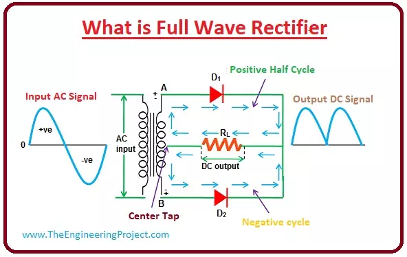
Hello friends, I hope you all are doing great. In today’s tutorial, we will discuss What is Full Wave Rectifier. Transformation of alternating current into the direct current is known as rectification. This conversion can be done by using a single diode or more than one diode. The diode that used for rectification is named as a rectifier. There are 2 main categories of the rectifiers, the first one is the half-wave and the other is full-wave rectifier. In half-wave rectification circuitry, there is only single diode is used to convert alternating current into the direct current. So it can very easily design for rectification. But it has one drawback that it converts one half of the AC wave into direct current. Due to this, there is a higher power loss in this circuitry. This rectifier is also not suitable for such applications where pure direct current is required. For full-wave rectification full-wave rectifier was introduced, that used more than one diode and converts complete AC waveform into the direct current. In today's post, we will have a look at its circuitry, comparison with other rectifiers, uses and some other related terms. So let's get started with a What is Full Wave Rectifier.

What is Full Wave Rectifier

  • The full-wave rectifier is such circuitry that transformed full sine waveform of the alternating current into the direct current.
  • You can see from the given diagram that the rectifier circuitry transformed the complete alternating waveform into the direct current.
  • There are 2 main types of full-wave rectification circuitries, first, one is centred tapped and other is bridge rectifier.
  • We discuss both of them with the detailed.
  • First, we discuss centre-tapped rectifier circuitry, to study this rectification first we discuss the centre-tapped transformer that is the important component of the centred tapped rectification circuitry.
Center Tapped Transformer
  • As we already know that there are 2 main windings of the transformer, the first one is primary and other is secondary.
  • If we connect an extra conductor at the center of the secondary winding, then the transformer is known as the centre-tapped.
  • This transformer works like a normal transformer, but it provides an additional feature to the transformer.
  • That is the voltage coming from the primary side to the secondary, will divide into 2 parts.
  • One portion at the secondary is a positive half-wave and other is a negative half-wave, our total output voltage will be the sum of these 2 voltages.

Vt = (V1 + V2)

  • This feature of the centred tapped transformer is used in the rectification process.

Center Tapped Full Wave Rectifier

  • In this type of the rectification circuitry, there is one centre-tapped transformer and 2 diodes are used for conversion of ac to dc.
  •  You can see from the circuitry that the input alternating supply is provided to the primary winding of the transformer and the at the secondary side an extra conductor is connected at the center of the secondary winding.
  • The central conductor divides the secondary winding into 2 parts, the first part of the secondary winding is connected with the diode (Dx) and other part connected with the diode (Dy).

  • Both of these diodes are also connected with the common resistor RL, that is load resistance it connect with the transformer by the tapped conductor.

Working of the Center Tapped Full-Wave Rectifier

  • This rectifier circuitry used a centre-tapped transformer for the conversion of the alternating current into the direct current.
  • When the voltage comes at secondary winding from the input windings it distributed into the 2 parts first one is positive and other is negative.
  • When the first half of the sine wave comes at the point A of the secondary it is at a positive potential and point B is at a negative potential, and the centre conductor is at 0 voltage level.

  • The point A is joined with the anode of the diode Dx and the point B is joined with the cathode of the Dx, this assembly tells that the diode Dx is forward biased condition, and current starts to flow.
  • You can see from the circuitry that point B is joined with the anode of the Dy and point A of the secondary windings is connected with the cathode of the Dy.
  • So diode Dy has reversed mode in the positive half of the supply and current does not flow through Dy.
  • This rectified current than goes to load resistor RL, and then to the secondary winding.
  • We can conclude that when positive half of the input comes then there will be zero current through Dy, as it is reversed biasing and Dx is in forward biasing so current passes through this diode.
  • When negative half comes at the secondary winding, the Point A is at a negative potential, and point B is at a positive potential.
  • The negative point A is joined with the anode of the Dx and positive point B is linked with the cathode of the Dx.
  • The diode Dx is in reverse mode so current does not pass through it.
  • The positive point B is joined with the anode of the diode Dy and point A is joined with the cathode of the Dy.
  • The diode Dy is now forward biasing so current will flow this diode.
  • Due to the reverse biasing of the diode Dx, during negative half, the current does not pass through the upper portion of the circuitry and current flows in the lower part.
  • So, in case of the negative half of wave-current pass through the Dy that is in the forward-biased state.
  • In conclusion, we note that the diode Dx operates in the positive half of the input supply and Dy operates in the negative half of the supply.
  • In this way, both parts of the input converted into the dc voltage. The given diagram explains the complete conversion of the input supply.

Full Wave Bridge Rectifier

  • It is the other category of the full-wave rectifier circuitry, in this circuitry, there are 4 diodes are connected in bridge-like arrangements, and converts ac input supply into the direct current supply.
  • Its main benefit is that there is no need of special centre-tapped transformer for this circuitry, that makes it simple and less costly.
  • We can see from the circuitry that 4 diodes are connected in a sequence, and only 2 diodes work for each half of the input supply.
  • When there is positive half at the circuitry diode D1 and D2 will operate and negative half diodes D3 and D4 will work.
Positive Half-cycle
  • When positive half of the input sinewave comes than diodes D1 and D2 works and positive half of the supply converts into the dc. The given diagram shows the direction of the current.
Negative Half-cycle
  • During the negative half of the supply only diodes, D3 and D4 will operate as they are in the forward-biased direction.
  • As D1 and D2 work in the positive half and the D3 and D4 works in the negative half, our output will be full-wave dc.
So, it is the detailed article on the full-wave rectifier, if you have any question ask in comments thanks for reading.

What is Zener Diode? Definition, Symbol, Working & Applications

Hello friends, I hope you all are doing great. In our previous lectures, we have studied two types of diodes i.e. Basic PN diode and Schottky Diode. Today, we will discuss the third type of diode i.e. Zener Diode.

Zener Diode was invented by the American engineer Clarance Melvin Zener, so it's named after him. The specialty of the Zener diode is that it can operate in both forward-biased and reversed-biased directions. In today's post, we will have a look at its working, features, ratings, construction and applications. So let's get started with what is the Zener Diode.

What is Zener Diode?

  • The Zener diode is a special diode, that enables the current to flow not only from the positive terminal (anode) to the negative terminal (cathode) but also in the opposite direction.
  • The doping of the Zener diode is more than the conventional diode, so its depletion part has less area.
  • The general diode does not operate in the reverse biased condition but Zener diodes are specially manufactured for reverse-biased operation.
  • Zener diode is mostly used in types of electronic devices like computers, laptops etc, it is the basic component of the electronic circuitries.
  • It is used for power stabilizer circuitries to maintain the voltage level for a particular device.
  • Zener diode also provides protection to any circuitry from over-voltage, particularly from ESD (electrostatic discharge). In ESD the current flows suddenly among two charged points by a short circuit or breakdown of insulation.

Breakdown in Zener diode

  • There are 2 main breakdown areas in the Zener diode.
    • Avalanche Breakdown
    • Zener breakdown
  • Let's discuss both of them one by one in detail.

Avalanche breakdown

  • This type of break-down not only exits in the Zener diode but also in the general diode due to higher voltage in reversed biased conditions.
  • When the diode is in the reversed biased condition the minority charge carriers get larger energy from the source and move fastly.
  • The high-speed charge carriers collide with the other particles and remove more electrons from the atom. These are traveling at a higher speed they also eliminate more electrons from other atoms.
  • Due to the larger quantity of electrons, the backward current will flow from cathode to anode, in some conditions the general diode can be damaged.
  • But the Zener diode may not burn because they are sketched to operate under those conditions.
  • The avalanche breakdown voltage for the Zener is six volts.
  • The given diagram explains the avalanche breakdown voltage.

Zener Breakdown

  • This type of break-down appears in the high doping diode like Zener, as this diode has less depletion area due to higher doping.
  • When the voltage provided to the diode increases, in a thin depletion area highly effective electrical field is established.
  • When the reversed polarity voltage almost equals the Zener voltage, the electric field in the depletion portion is such strong that it pulls out the electrons from their valance shells.
  • The outermost shell electron that gets enough power from the field will break out from the effect of the mother atom.
  • The outermost shell electron that breakout from the effect of its mother atom will move freely.
  • Due to the free drift of this election, the reverse current will flow in the diode.
  • The less increment in the voltage will cause to move current very fastly at the Zener breakdown portion.

 Difference between the Zener and Avalanche Breakdown

  • Zener break-down occurs at less value of revered biased voltage while avalanche at the higher reversed biased voltage.
  • Zener breakdown occurs only in the Zener diode as they have less area of depletion portion.
  • The break-down area is such a region in which the Zener diode usually works.

Zener Effect

  • Zener Effect is the category of the electric failure (breakdown) that exits in reverse biasing PN junction the strong statice field allows the electrons to move from the valance band to the conductive band of a semiconductor.
  • Its name is due to the use of this factor in the operation of the Zener diode.

Zener Diode I-V Characteristics

  • Zener diode works in the reversed biasing conditions is reversed biased mode its anode is connected with the negative terminal and cathode with the positive terminal of supply.
  • In the given diagram, the reversing biasing effect of the Zener is shown in the curve between the current and the voltage.
  • When we provide voltage to the Zener a small amount of the leakage current flows in the diode, till that point the applied voltage is less than the Zener voltage.
  • When the value of applied voltage approaches the Zener voltage then a large amount of the reversed current flows in the diode and the curve suddenly changes its state from the flat to vertical.
  • Due to the instant increase in the current value, the breakdown that happens in the diode is called the Zener breakdown.
  • But, the Zener diode manifests a restrained breakdown that does harm the component.
  • The quantity of the Zener breakdown voltage fluctuates according to the doping level of the diode.
  • If the doping level of the diode is larger then breakdown occurs at a lesser voltage.
  • If doping is less then breakdown happens at the higher value of the revered supplied voltage.
  • Usually, the value of the Zener voltage for the diodes is (1.8) volts to (400) volts.

Advantages of Zener Diode

  • There are some advantages of the Zener diode over the general diode that make it effective to operate in high voltage conditions.
    • Its power consumption capability is higher than the normal diode.
    • Its efficiency is very high.
    • It is available in a smaller size.
    • It is a less expensive diode.

Applications of Zener Diode

  • These are some applications of the Zener diode.
    • It is commonly used as a voltage reference device.
    • It is used in voltage regulators.
    • It is used for switching purposes.
    • Zener diode is an important part of the clamp and clipping circuitries.
    • It is used in many security circuitries.
    • It is also used in electronic devices like mobile laptops, computers, etc.

So, it is a detailed article on the Zener diode, I have each and everything related to the Zener diodes. If you have any questions about it ask in the comments. Thanks for reading take care until the next tutorial.

Schottky Diode: Definition, Working & Characteristics

Hello friends, I hope you all are doing great. In our previous lecture, we studied the Basic PN Diode in detail and today, we will discuss a special type of diode called Schottky Diode. This diode was designed by the German physicist Walter H. Schottky, so it's named after him, thus called Schottky.

This diode is mostly used in radio frequency (RF) circuits or in power supplies. So let's get started with the basics of Schottky Diode:

Schottky Diode

  • Schottky Diode (also called Schottky Barrier Diode or Hot Carrier Diodes), discovered by German physicist Walter H. Schottky, is a special type of diode in which the P-layer(of PN junction) is replaced by the metal layer(i.e. Aluminium, Tungsten, Molybdenum, Platinum, Chromium etc.), while the N layer is of silicon(semiconductor - same as in normal diode).
  • As we discussed earlier, the PN Junction of a normal diode is composed of a P-type semiconductor and N-Type semiconductor material, while the Schottky Diode has a metal on one side of the junction and an N-Type semiconductor on the other side.
  • You can see in the above figure, we have a Metal Region instead of a P-Type Region, so we can say the junction of the Schottky diode is a doping result of metal and semiconductor(Silicon).
  • This Metal-to-Silicon Junction generates a potential barrier of 0.15-0.3V, which is 0.7V for a simple diode.
  • In Schottky Diode, the number of electrons is greater than the number of holes and thus electrons are solely responsible for the flow of current, and thus termed as Unipolar, while in a normal diode, both holes & electrons are equally responsible for the current flow and thus termed as Bipolar.
  • The Schottky diode symbol is slightly different than that of a normal diode, as it has a slight bend on both sides of the straight bar.
  • Examples of Schottky diodes are BAT49 and 1N5711, manufactured by ST Microelectronics.

Why use Metal-to-Silicon Junction?

The Schottky diode has a Metal-to-Silicon Junction instead of a simple PN Junction, which gives it many advantages over a simple diode.

  • The potential barrier of a simple PN diode is 0.7V for silicon, which makes it useless for small signals i.e. radio frequency circuits.
  • On the other hand, a metal-to-silicon junction develops a potential barrier of around 0.15-0.3V, making it ideal for low-valued signals.
  • The potential barrier of a Schottky diode depends on the metal used and the amount of doping in the N-Type region.
  • Because of low voltage consumption, its response rate is high and thus used in fast switching applications.
  • If we increase the doping of a semiconductor, it will decrease the width of the depletion region, thus lowering the potential barrier.

Schottky Barrier

  • The depletion region created after the doping of metal & semiconductor (as in the Schottky diode) is called Schottky Barrier.
  • In simple words, the Schottky barrier is a minimum Potential Energy required for electrons to cross the barrier.
  • Once the P.E. of electrons exceeds a certain limit (depending on doping), they overcome the Schottky barrier and start flowing across the Schottky diode.
  • The Schottky barrier's width is quite smaller as compared to the depletion region in a normal diode.
  • It normally takes 0.15V to 0.3V to overcome the Schottky Barrier, while for normal depletion regions, it takes 0.6V to 0.7V.
  • There are further 2 types of Schottky barriers:
    • Rectifying Schottky barrier.
    • Non-rectifying Schottky barrier.

 Schottky Diode Energy Band

  • The potential energy level of electrons outside the material is known as the Vacuum level.
  • The amount of energy needed to move electrons from the Fermi level to the vacuum level is known as the work function.
  • The value of this energy (work function) is different for metals and semiconductors.
  • So the electrons in N-type semiconductors have a larger value of P.E than the electrons in metals.
  •  Let's see the diagram of the energy band of Schottky diode:

Schottky diode Characteristics Curve

  • Now, let's discuss the voltage and current characteristics of the Schottky diode.
  • It has low forward voltage loss that's why its characteristic curve is close to current axes as compared to normal diodes.
  • When the applied voltage to the Schottky diode exceeds 0.15-0.3V, the diode becomes forward-biased.
  • Schottky Diode has a Low Reverse Breakdown Voltage as compared to the normal diode and if this limit exceeds, it may damage the component permanently.

Schottky Diode Vs Normal Diode

Schottky Diode Vs Normal Diode
No. Schottky Diode Normal Diode
1 Metal-Semiconductor Junction PN Junction
2 Low Forward Voltage Loss (0.2V - 0.3V) High Forward Voltage Loss (0.6V - 0.7V)
3 High Reverse Saturation Current. Low Reverse Saturation Current.
4 Schottky Barrier created. Depletion Region created.
  • In the below figure, you can see the difference between Schottky Diode & normal diode:

Schottky Diode Advantages

  • It has a low forward voltage drop.
  • It has a fast response time.
  • It has a fast recovery time, thus highly efficient.
  • It has a high current density and thus can handle high current at low voltages.

Schottky Diode Disadvantages

  • It has a high reverse saturation current.

Schottky Diode Applications

There's a long list of Schottky Diode's applications, here I've mentioned a few of them:
  • It's used in radio frequency appliances.
  • It's used in circuits of Logic Gates.
  • It's used in designing rectifiers.
  • It's used for controlling reverse current in power supplies.
  So, that was all about Schottky Diode, if you still have any questions, please ask in the comments section below. Take care.
Syed Zain Nasir

I am Syed Zain Nasir, the founder of <a href=https://www.TheEngineeringProjects.com/>The Engineering Projects</a> (TEP). I am a programmer since 2009 before that I just search things, make small projects and now I am sharing my knowledge through this platform.I also work as a freelancer and did many projects related to programming and electrical circuitry. <a href=https://plus.google.com/+SyedZainNasir/>My Google Profile+</a>

Share
Published by
Syed Zain Nasir