A Detailed Guide on PCB Fabrication Process
Hi Friends! Happy to see you around. Thank you for clicking this read. In this post today, I’ll document a detailed guide on the PCB fabrication process.
PCB is commonly used in modern electronics. If you uncover the TV set and have a look inside, you’ll find a printed circuit board, electrically connecting components on the board. There are copper traces incorporated on the board to electrically connect the components and provide the current flow from one part to another.
These printed boards make devices precise and compact that are capable of doing more functions than the devices where the end to end wiring is used.
Circuit boards are divided into three main types. Let’s discuss each type one by one so you can better understand the structure of each type before employing them in the relevant application.
If you don’t want to undergo this intimidating fabrication process of the board, you can get help from the online PCB manufacturers. We are quite satisfied with PCBWay services, so I am going to recommned this one.
PCBWay is a great place to get your ready-made PCBs. Simply submit your details, and they will return the PCB quote for the given project, which you’ll get within 2-5 business days. They have a team of professionals, ready to guide you throughout the process.
Main Types of Printed Circuit Board
Circuit boards are categorized into three types.
Single-sided Circuit Boards
Single-sided PCB, also called single layer PCB, is composed of woven glass epoxy material which is incorporated with copper traces on one board side and another board side is utilized to put components on the board.
These copper traces electrically connect the different components on the board.
Double-sided Circuit Boards
Double-sided PCB, also called two-layer PCB, is made of the same rigid woven glass epoxy material that is used in single-sided PCB, and there’s a little difference. Here both board sides are incorporated with the copper traces. And traces are kept with different thicknesses depending on the application.
Multiple-sided Circuit Boards
In Multi-layer PCB copper foil is employed rather than a copper coating. This copper foil helps in the construction of different layers until you reach the required number of layers.
Main Parts of PCB
Let’s elaborate on the basic parts of the PCB before documenting the fabrication process.
Substrate
This is termed as the PCB skeleton – the most fundamental structure of the board. Fiberglass is utilized to construct the substrate material. Fiberglass confirms the core strength, making board strong, stern, and solid.
Copper Layer
The following part is the copper layer. Depending on the PCB type, copper coating or copper foil is employed on one side or the two sides of PCB. This copper layer is used to provide an electrical connection between the board’s components. This is like the nervous system of the brain that contains neurotransmitters to communicate with the body muscles.
Solder Mask
On the third number comes the solder mask. It is a defensive layer composed of a polymer that goes about as a PCB skin. It helps in securing the copper layer. It also helps protect the board from short-circuiting.
Silkscreen
Silkscreen, also called legend or nomenclature, is the last part of the PCB. It is normally smeared on the board’s component side. This layer is utilized to demonstrate logos, switch settings, part number, test points, and component reference.
PCB Fabrication Process
In this part, we’ll demonstrate the PCB fabrication process in detail.
Step 1: The Initial Design
Everything begins with the fundamental design. A comprehensive PCB design is made on the software. There are multiple software used for the PCB design including Altium Designer, Eagle, OrCad, Pads, Proteus or KiCad
When the design is made, the document is then exported. Most manufacturers support the extended Gerber file… so be sure your final document is exported in the Gerber file.
It is important to know that different software comes with different Gerber file generation steps, however, all these software constitute comprehensive information about copper tracking layers, drill drawing, component notations apertures, and other options.
Step 2: The Print Process
The PCB is printed using the plotted printer. It produces the resultant film which is made of different layers. The black ink shows the conductive copper traces on the other hand the clear ink represents the non-conductive portions.
This is used for inner layers. On the layers outside this pattern is switched for example the clear ink demonstrates the conductive copper traces and black ink shows the non-conductive regions.
Step 3: The Substrate Material
Recall, the substrate is considered as the skeleton of the PCB that is made of fiberglass. This fiberglass behaves like an insulating material that is used to connect the various elements.
Step 4: The layers
In the fourth step, resist is made that is composed of photosensitive film. Photo-reactive chemicals are used in this resist. When these chemicals come under the UV light, it helps in hardening the resist.
Step 5: Hardening the Photoresist Layer
In this step, underlying copper pathways are revealed. Which is achieved by hardening the photoresist layer. The photoresist layer gets hardened when a combination of resist and laminate is exposed to the UV light.
Step 6: Removal of Unused Copper
In this step, unwanted copper is removed. Unwanted copper is removed using the alkaline solution. While you’re at this process, be careful that it doesn’t affect the photoresist layer.
Step 7: Inspection
Optical inspection and layer alignment are done in this step. Both the outer and inner layers are aligned using the holes.
Everything is aligned using the punch machine.
Step 8: Lamination Process
At stage 8, both outer and inner layers are pushed together for the cover. These layers are fused whenever they are examined, ensuring they are without any defect.
These layers are aligned using the Prepreg made of epoxy resin. Metal clamps are used to set everything in place. The Prepreg material is covered with the substrate and copper foil. Everything is kept in place using pins and the mechanical press is employed to punch everything together. When heat and pressure are applied to the epoxy material, it melts down causing layers to fuse together. The actual PCB is then removed by removing the pins and press plates.
Step 9: Drilling Process
After stage 8, the drilling process is carried out. An X-ray machine is used to locate the drill spots before applying drilling on the layers. Holes are created using a computer-guided drill. Leftover copper is then removed after the drilling process is completed.
Step 10: PCB Plating
After the drilling process, a specific compound is applied to weave all layers together. This process is called PCB plating.
A series of chemicals are then used to cleanse the PCB layers. The copper layer is applied between the drilled holes and on the top of the layer during this bathing process.
Step 11: Outer Layer Imaging
Another layer of photoresist is employed at the PCB outer layers once the PCB plating is done. This photoresist layer is then exposed to UV light which hardens this layer. In this process, again PCB plating is applied using certain chemicals that again helps in fusing the layers together.
The process is similar as we did in the last PCB plating process. The copper appears on the PCB outside layer is secured by the plating of tin which is developed around the outer layers.
Step 12: The Etching Process
The tin guard is created during the last process. During the etching of this outer layer, the tin guard is utilized to secure the copper layer. After this process, unused copper is removed while the tin guard developed during the last process still protects the copper present on the outside layer.
Step 13: Applying the Solder Mask
When the unused copper is removed it results in the making of proper PCB connections. In this step, we do solder masking. The final PCB panels now undergo the bathing process before we employ the solder mask. Ink proxy is used with the solder mask after the cleaning process has been finished.
Then the product undergoes the UV light which results in the removal of the unused solder mask. After this step, we put PCB in the oven that develops the green colors on the PCB panels.
Step 14: Final Surface Finish
In this step silver and gold materials are applied to produce the final surface finish. These materials ensure the core strength of the PCB layers and help in improving the elements bonding.
After plating the PCB layers with materials like silver and gold, silk-screening is applied. In this silk screening process the necessary details like manufactures marks, company ID, warning labels are then applied to the layers of PCB.
Step 15: Electrical Testing
In this step, electrical tests are applied to the PCB layers to confirm the functionality of the PCB layers. Two tests are applied… one is a circuit continuity test and the other is the isolation test.
Step 16: Final Cutting Step
In this final step cutting process is carried out the removes the PCB from the original pane. A CNC machine or V-groove is used to remove PCB from the original panel.
The final PCB is now ready to be used in an electrical project.
That’s all for today. I hope you’ve enjoyed reading this article. If you’re unsure or have any questions, you ask me in the section below. I’d love to help you the best way I can.
You’re most welcome to share your valuable suggestions and feedback around the content we share so we keep sharing quality content tailored to your exact needs and requirements. Thank you for reading the article.
Junction Field Effect Transistor (JFET) Simulation in Proteus ISIS
Hello Learners, hope you are doing well. I am here with a new tutorial. We'll discuss about
Junction Field Effect transistors. In this tutorial, we will learn the basic Introduction to JFET nad will also have a look at its practical Implementation and simulation in Proteus.
Basically, Junction Field Effect is a type of transistor, similar to Bipolar Junction Transistors but they have different characteristics due to some reasons as discussed below:
Introduction to JFET
We Define the JFET as:
"Junction Field Effect transistors or simply JFET is the semiconductor ,Voltage Control, three terminal device that is present in both configurations either N channel or P channel."
JFET are named so because the the operation of JFET relies on the Field of the input gate voltage thus they are voltage operated devices.
The Input of JFET is called
Gate whereas, the output is said to be
Drain.
Explanation about JFET
Junction Field Effect Transistors are important Devices in the world of electronics. They look similar to the transistors but are different in their Production.
Terminals of JFET:
JFET's have two Ohmic connections at either side of the channels. These channels are called
Source and
Drain. the Connection of Drain and source is said to be
Gate. This is the point where PN Junction is formed.
Source and Drain Collectively makes resistive path through which the current
Id passes due to the Voltage
Vds. The channel is semiconductor due to which current is passed equally well at both sides. But, because of the resistivity of the channel, the voltage becomes less Positive when we move from Drain to Source.
Subsequently, the PN junction contains the high reverse bias at Drain as compared to the Source. Thus, the a
Depletion Region is formed due to biasing whose width increase with the increase in the Biasing and vise Versa.
Configuration of JFET:
We know that Transistors are made by two type of materials i.e, N type and P type. The Terminals are connected by a current path between Drain and Source. these two terminals work as Collector and Emitter, respectively. Hence we observe two Configurations of JFETs:
- N-Type.
- P-Type.
Within the P-Type Configuration, we observe the doping of acceptors. hence holes are abundant in this region. by the same token, N- type configuration contain the doping of the electrons hence we get the faster conduction in N-Type region.
We'll use N type JFET for the experiment.
Types of JFET:
Base upon their Production, we classify the JFET in two types:
- Standard JFET
- Insulated Gate JFET
The 2nd type i.e, IGJFET is most Commonly called Metal Oxide Junction Field Effect Transistor or simply MOSFET.
Conduction of JFET:
JFET are unipolar Devices and their efficiency mainly depends upon the Conduction of holes and electrons in P-Channel and N-channel, respectively.
Implementation of JFET in Proteus ISIS
The Junction field effect transistors has very specific characteristics that can easily observed on the graph at a glance. Hence, let's start the simulation for best understanding.
Material Required:
- Junction Field Effect Transistor (2N3819)
- DC Power Supply
- Ground Terminal
- Current Probe
- DC Transfer Curve Analysis
Procedure for the characteristics of JFET:
- Fire up your Proteus Software.
- Pick Up the JFET from the Pick Library through the "P" button.
- Set the JFET on the working area.
- Foster the "DC" from the power Generation mood of the Proteus.
- Fix 1 DC power supply at the Gate Terminal and the other on the Drain Terminal.
- Pick the Ground terminal from "Terminal mode" and fix it with the Source.
- At this stage, the circuit should look like the picture given below:
- Place the Current probe taken from the side of the Proteus at the Drain.
One point must be clear here, the direction of the probe should be towards the drain showing that the current passes from the Current source towards the Drain terminal of JFET.
- Name the Gate source as "Vgs".
- Name the Drain power supply as "Vds".
- Mark the Current Probe as "Ids".
- Choose "Transfer" from the Graph mode at the left most bar of the Proteus.
- Click on the Working area and make a window of the "DC Transfer Curve Analysis".
- To get the output, we will drag the Id at the graph area.
- At the instance, we have to set the Graph according to our need. Truss, Double click the graph to edit the Properties.
- Set the Values according to diagram:
Now, when we simulate the graph by left click>simulate the graph, we find a simulation log.
- Simulate the graph through the Play button.
- Maximize the screen through left click at Graph>maximize and Observe the output.
Observations of JFET Characteristics:
- Vgs applied to the Gate Controls the Current flowing between Drain and the Source.
- No current flow through the Gate hence the Source current that is flowing out of the device is equal to the Drain current moving into the device.
Mathematically,
Is=Id
- We observe the four types of regions here:
- OHMIC Region: JFET acts like a voltage resistor when voltage VGS =0 because the depletion region at this point is very less.
- Pinch-off region: Resistance is maximum when Vgs is sufficient to cause the JFET to act as an open Circuit. This region is also called Cut-off region.
- Saturation Region: In this Region, the JFET becomes the Good Conductor and be controlled by Vgs. The Vds has very less effect.
- Breakdown Region: We observed that the in this region, the Vds becomes maximum and is controlled.
Advantages of JFET:
- They are replaced by the BJT because they are similar to BJT in characteristics like efficiency , robust, instant operation but are smaller than the equivalent Bipolar Junction Transistors. Thus they are better.
- Due to the size, they have less power consumption and low power dissipation, therefore are ideal to use in ICs and the CMOS range of circuit.
- They have extremely high input Impedance tat can be more than thousands.
Consequently, We learnt about extremely important features of the Junction Field Effect Transistor, Perform the experiments for the characteristics and observed the Advantages of JFETs.
Half Adder through XOR with AND Gate in Proteus ISIS
Hello Pupils! I welcome you to The Engineering Projects. I hope you are having a good day. In our previous lectures, we simulated almost all the DLD Logic Gates i.e. AND, OR, NOT, NOR, NAND, XOR and XNOR. I hope now you must have a complete understanding of the logic gates and their working.
Now, it's time to have a look at the reason for inventing these logic gates. These DLD logic gates are used to design different numerical modules i.e. adder, subtracter, multiplexer, de-multiplexer, encoder, decoder etc. These arithmetic modules are normally used in electronic products i.e. a simple microcontroller has numerous adders/subtractors for properly calling the registers' addresses.
So, from today onward, we are going to discuss these applications of logic gates one by one. Today, we will focus on the basic one i.e. Half Adder. First, we will understand its working and later will simulate it in Proteus.
Let's have a look at what we'll learn today.
- What is an Adder?
- What is Half Adder?
- Truth Table of Half Adder.
- Half Adder Simulation in Proteus.
- Advantages of Half Adder.
- Disadvantages of Half Adder.
Let's start the Learning.
What is Adder?
- In DLD, an Adder is a simple digital circuit, designed using logic gates and is used to add binary numbers(normally bits).
- Advance Adders can also add other number systems i.e. Binary Coded Decimal, HexaDecimal etc.
- There are two types of Adders, named:
- Half Adder
- Full Adder. (We will cover it in the upcoming lectures)
Now, let's have a look at the definition of Half Adder:
What is Half Adder?
- A Half Adder is a simple arithmetic electronic circuit, designed using logic gates to add two binary numbers.
- A Half Adder produces two Outputs of 1-Bit each. These outputs are the Sum and Carry of the added numbers.
- The numbers being added(i.e. inputs of Half Adder) are called augend and added.
- A simple Half Adder is shown in the below figure:
- We will understand the working of Half Adder in the next section but for now, we can see in the above figure, the Adder circuit has two inputs and 2 outputs.
- The first output is Sum Bit and the second one is Carry Bit.
- A simple Block Diagram of Half Adder is shown below:
Logical Circuit
In order to design a DLD Half Adder, we will need to use the following two logic gates:
- XOR Gate
- AND Gate
If we recall from our previous lectures on logic gates, the XOR Gate is used to provide the Sum of the Inputs, while the AND Gate provides the Carry of the Inputs. So, by combining these two gates, we can easily get both the Sum and the Carry.
Mathematically,
SUM = A XOR B
CARRY = A AND B
- Here's the Truth Table of XOR Gate:
| A |
B |
Z |
| 0 |
0 |
0 |
| 0 |
1 |
1 |
| 1 |
0 |
1 |
| 1 |
1 |
0 |
- The Truth Table of AND Gate is given below:
| A |
B |
Y
|
| 0 |
0 |
0 |
| 0 |
1 |
0 |
| 1 |
0 |
0 |
| 1 |
1 |
1 |
Let's move towards the Practical implementation of Half Adder in Proteus ISIS.
Simulation of Half Adder in Proteus
To design the circuit of Half Adder, we need the following components:
Components Required:
- AND Gate.
- XOR Gate.
- Logic toggle.
- LED.
- Ground Terminal.
Circuit Diagram of Half Adder
- Select the first four components from the Proteus Library.
- Place the XOR Gate and AND gate in the Proteus Workspace.
- Connect the Logic Toggles on the Inputs of the XOR Gate.
- Join the inputs of AND Gate with the Inputs of XOR Gate.
- Connect the LEDs with the output Terminals of both Gates.
- Add the ground terminal with both LEDs.
- The below figure shows the Half Adder Circuit in all possible scenarios:
- Here's the Truth Table of Half Adder:
| Input |
Output |
| A |
B |
Sum
|
C0 |
| 0 |
0 |
0 |
0 |
| 0 |
1 |
1 |
0 |
| 1 |
0 |
0 |
0 |
| 1 |
1 |
1 |
1 |
Advantages of Half Adder
- Half Adders are simple in construction
& easy to design.
- We can get a Half Subtractor simply by inverting the circuit.
Disadvantages of Half Adder
- There is no mechanism to use the carry in the next addition.
- Can perform very specific functions.
So, that was all for today. I hope you have enjoyed today's lecture. Today, we designed the Half Adder using AND and XOR gates. In the next lecture, we will design the Half Adder using Universal Gates i.e. NAND and NOR gates. Till then, take care. Have fun!!!
Half Adder with Universal Logic Gates
Hello Pupils! I welcome you to The Engineering Projects. I hope you are having a good day. In our previous lecture, we discussed Half-Adder Circuit Designing with XOR and AND logic gates. Today, we are going to design the same circuit using universal logic gates i.e. NOR and NAND gates.
We are going to learn the following topics, in today's lecture:
- What is Adder?
- What is Half Adder?
- How can We make Half Adder Circuit through NAND Gate?
- How can We make Half Adder through just NOR Gate?
Hence without wasting time, Let's find all the Answers.
What is Adder?
As we discussed in the last lecture, the DLD Adder is a simple electronic circuit, used to add binary numbers in bit form.
There are two types of DLD Adders, named:
- Half Adder
- Full Adder
In this article, we'll focus on the Half Adder only.
What is Half Adder?
Let's recall it as well from our previous lecture, a Half Adder is a simple electronic circuit, designed with logic gates and is used to add two binary numbers. It generates two output bits i.e. Sum Bit and Carry Bit.
In our previous lecture, we designed the Half Adder using two types of Logic Gates i.e. AND and XOR but today, we are going to use a single type of logic gate(Universal Gate) to design a Half Adder. As we know there are two universal gates in DLD i.e. NOR and NAND. So, we will design the Half Adder circuit with both of these Universal Gates, shown in the below figure:
Truth Table of Half Adder
- The Truth Table of the Half Adder is shown in the below table:
| Input |
Output |
| A |
B |
Sum
|
C0 |
| 0 |
0 |
0 |
0 |
| 0 |
1 |
1 |
0 |
| 1 |
0 |
1 |
0 |
| 1 |
1 |
0 |
1 |
Half Adder with NAND Gate
Let's first recall the NAND Gate:
"A NAND Gate is an inversion of AND Gate and gives LOW output if all of its Inputs are HIGH, otherwise gives HIGH output".
The Truth Table of NAND Gate is shown below:
| A |
B |
(A.B)' |
| 0 |
0 |
1 |
| 0 |
1 |
1 |
| 1 |
0 |
1 |
| 1 |
1 |
0 |
Let's rush towards the Proteus software to run our Half Adder.
Components Required
We will need the following components to design Half Adde circuit in Proteus:
- NAND Gate
- Logic Toggle
- LED
- Ground Terminal
Proteus Simulation of Half Adder
- Here's the Circuit Diagram of the Half Adder with the NAND gate in Proteus:
- For designing the Half Adder circuit, we'll need 5 NAND gates in total, so get them from Proteus Library and place them in the Workspace, as shown in the above figure.
- I have used two Logic States at the Inputs and two LEDs at the Outputs.
In order to understand this Half Adder circuit, let's create a truth table of output at each NAND Gate:
| Input |
Output |
| A |
B |
1 |
2 |
3 |
4(SUM) |
5(CARRY) |
| 0 |
0 |
1 |
1 |
1 |
0 |
0 |
| 0 |
1 |
1 |
1 |
0 |
1 |
0 |
| 1 |
0 |
1 |
0 |
1 |
1 |
0 |
| 1 |
1 |
0 |
1 |
1 |
0 |
1 |
Half Adder with NOR Gate
Let's recall the NOR Gate from our previous lecture:
"A NOR Gate is an inversion of the OR Gate and gives HIGH Output only if all of its Inputs are LOW, otherwise it gives LOW".
The Truth Table of NOR Gate is as follows:
| A |
B |
(A+B)’ |
| 0 |
0 |
0 |
| 0 |
1 |
0 |
| 1 |
0 |
0 |
| 1 |
1 |
1 |
To implement the Half Adder with NOR Gate, we are going to use the below components:
Components Required:
- NOR Gate.
- Logic Toggle.
- LED.
- Ground Terminal.
- Connecting wires.
Proteus Simulation of Half Adder
Here's the circuit diagram of the Half Adder with NOR logic gate:
As you can see in the above figure, we have used 5 NOR gates in total and have placed logic states at the inputs and LEDs at the outputs.
Here's the truth table of Half Adder with NOR Gate:
| Input |
Output |
| A |
B |
1 |
2 |
3 |
4(SUM) |
5(CARRY) |
| 0 |
0 |
1 |
1 |
1 |
0 |
0 |
| 0 |
1 |
0 |
0 |
1 |
1 |
0 |
| 1 |
0 |
1 |
0 |
0 |
1 |
0 |
| 1 |
1 |
0 |
0 |
0 |
0 |
1 |
So, that was all for today. In the next lecture, we will discuss the 2-Bit Full Adder in detail and will simulate it in Proteus. Thanks for reading.
6 Ideas for Establishing an Engineering Consulting Firm
Hello friends! Welcome to another useful article of
The Engineering Projects. I hope you are having a shinning day. Let's add some reproductive information in your day. Today we'll grasp about the establishment skills in Engineering Consultant Firm. Consequently, we'll learn about 6 tremendous ideas for the Establishment an Engineering Consultant.
Starting any business can be difficult. As a matter of fact, some individuals state that around a third of new enterprises fail within the first year of operation. From there, this does not get any easier. These numbers increase to half by the second year of running a business.
This might put you off when you decide to start your engineering consulting firms. However, you can make an engineering consulting company a success by considering the below ideas:
Be Strategic About Scheduling and Quoting
Quoting projects for the first time is challenging, though asking individuals who carried out the same tasks would be great to start. The best thing you may do for your clients is to meet them where they are. Many of your clients will be entrepreneurs who have a specified budget for work they need to be completed.
Scheduling projects will also depend on your bandwidth. It will not benefit anyone when you have a lot of work that you can hardly handle. If you can quote for more time, clients will be happier when you deliver their projects early.
Learn How to Reduce Costs
Most organizations choose to implement CMMS in an attempt to decrease maintenance costs as well as enhance their bottom line in different ways. Therefore,
what is CMMS software? Well, the software is a system, which facilitates the upkeep operations and centralizes maintenance information.
This will help optimize the availability and utilization of physical equipment, such as plant infrastructures, communications, vehicles, and machinery. Your CMMS can also help you decrease the total number of reactive maintenance and unplanned breakdowns of your machines.
Gain Skills
When starting an engineering consulting company, you will need the necessary skills. After you decide on the value proposition, you need to gain the right skills and necessary knowledge.
You should also be a degree holder. Engineers with a degree certificate are likely to establish their own firms. Later on, they may pursue a degree in management so as to acquire skills and learn how to work.
Have a Plan
When writing a plan for your engineering consulting company, you may include an executive summary, which explains your experience.
Moreover, you may include the goals of your business and an explanation regarding your engineering company. You can as well offer detailed monetary information about your engineering consulting company.
Delegate Work
Regardless of which maintenance strategy you have, your maintenance team may need to deal with unplanned work. Human error, machine malfunctions, natural disasters, and accidents are some of the things you may not avoid completely.
However, assigning projects to work orders will help technicians choose which work should be completed first. This may be important in emergencies when you require every hand on deck. In such a situation, you may use a mobile CMMS so as to send a push notification and develop a work order to every technician.
Consider Content Marketing
Inbound marketing is constructed around four different phases, including converting, delighting, closing, and attracting. Basically, you have to lure visitors to your site, close sales, delight clients, and convert customers into quality leads. The top-secret to effective inbound marketing lies in using the right messaging and content to target the correct audience in real-time. This will need a working knowledge of buyer personas.
When it comes to engineering consulting companies, buyer personas tend to be disparities on decision-makers in construction firms, real estate developers, architectural organizations, and government agencies. In your buyer persona, you may include other useful details related to purchasers' motivations and demographic profile.
Concluding Remarks!
As an engineer, it’s not a must you work in an established engineering company. Immediately you have the experience to work in your specialty, you may launch your own firm.
Whether you are a structural, mechanical, electrical, civil, and computer engineer, you may start a new engineering consulting firm. If you want to develop many engineering projects and establish a client list, you can consider some of these ideas.
Introduction to Arduino Nano 33 IoT
Hi Guys! Hope you’re well today. Happy to see you around. In this post today, I’ll walk you through the Introduction to Arduino Nano 33 IoT.
Arduino Nano 33 IoT is mainly used in basic IoT applications. The Internet of things is one of the most exciting and robust developments in the field of information technology.
Using this technology you can interface a network of physical things with software, sensors, or other technologies to develop communication and data exchange between devices and other systems using the internet.
For example, you can control the room temperature by interfacing the sensors in your rooms with your smartphone through WiFi. Traditional systems including control systems, wireless sensor networks, embedded systems, and home automation all contribute to activating the internet of things.
Over the past two decades, networking technologies have been commonly restricted to traditional devices like desktop computers, laptops, and more recently tablets and smartphones. With the inception of innovative technologies, IoT continues to cover scores of devices into the network including medical devices, household appliances, vehicles, electric motors, traffic controls, street lights, smart TVs, and much more.
At Arduino, you can either generate your own Arduino Access Point or connect the board with any existing WiFi network.
I suggest you buckle up, as I’ll detail the Complete Introduction to Arduino Nano 33 IoT covering pinout, pin description, features, programming, and applications.
Let’s get started.
Introduction to Arduino Nano 33 IoT
- Arduino Nano 33 IoT is a microcontroller board based on low power Arm® Cortex®-M0 32-bit SAMD21.
- This board features a u-blox, the NINA-W10 that is a low-power chipset mainly employed to develop Bluetooth and WiFi connectivity.
- With this device, you’ll also get a 6 axis IMU that makes this device an ideal fit for pedometers, vibration alarm systems, and the relative positioning of robots.
- Moreover, this device contains a Microchip® ECC608 crypto chip that stores the cryptographic keys in hardware and guarantees secure and safe communication.
- Visit WiFiNINA library reference page and get a hold of several certain examples available for Arduino Nano 33 IoT.
- This device is completely compatible with the Arduino IoT cloud. You can use the Arduino IoT cloud for free – a simple and efficient way to guarantee safe and secure communication over all connected devices.
- There are 14 digital I/O pins, 8 analog pins, and 11 PWM pins incorporated on board.
- The board contains Flash memory of 256KB. This memory is used to store the Arduino Program (sketch). While the SRAM memory is 32KB that is used to produce and manipulate variables when it runs. There is no EEPROM available on this board.
- The clock frequency of an oscillator is 48MHz which is used for the synchronization of all internal functions.
Arduino Nano 33 IoT Pinout
The following figure shows the pinout diagram of Arduino Nano 33 IoT.
The board contains two LEDs i.e. one is a built-in LED connected to pin 13 of the board and the other is the power LED that turns on when power is supplied to the board.
Arduino Nano 33 IoT Pin Description
This is the little introduction to Nano 33. In this section, we will detail the pin description of each pin incorporated on the board.
Digital Pins
The Nano 33 board contains 14 digital pins that you can use as input or output depending on the requirement. These pins receive only two values HIGH or LOW. When pins receive 0V they are in a LOW state when they receive 5V they remain in the HIGH state.
Analog Pins
This board carries 8 analog pins. These pins can receive any value in contrast to digital pins that receive only two values i.e. HIGH or LOW.
PWM Pins
The Nano 33 board features 11 PWM pins. These pins, when activated, generate analog results with digital means.
SPI Pins
This is the serial peripheral interface that is used to develop communication between a controller and other peripheral devices like shift registers or sensors. Two pins: MISO (Master Input Slave Output) and MOSI (Master Output Slave Input) are incorporated for SPI communication between devices. These pins are used to send or receive data by the controller.
I2C Pins
The Nano 33 contains the I2C two-wire communication protocol. It carries two pins SDA and SDL. The SDA is a serial data pin used to carry the data while SCL is a serial clock line used to synchronize all data transfer over the I2C bus.
The I2C protocol is used to develop communication between two or more integrated circuits.
UART Pins
This board supports UART serial communication protocol with two pins Tx and Rx. The Tx pin is a transmission pin used to transmit serial data while Rx is a receiving pin mainly employed to receive the serial data.
Arduino Nano 33 IoT Features
- Microcontroller = SAMD21 Cortex®-M0+ 32bit low power ARM MCU
- Secure Element = ATECC608A
- Oscillator = 48 MHz
- Radio module = u-blox NINA-W102
- Input Voltage (limit) = 21V
- Flash Memory = 256KB
- SRAM = 32KB
- EEPROM = no
- DC Current per I/O Pin = 7mA
- Operating Voltage = 3.3V
- Digital I/O pins = 14
- PWM Pins = 11
- Analog Pins = 8
- External Interrupts = All digital pins
- Size = 18x45 mm
- UART = 1
- SPI = 1
- I2C = 1
- Weight = 5gr.
Programming
Arduino.cc has introduced an official software Arduino IDE to program all boards of the Arduino Family. The C and C++ languages are used in this software to program the Arduino boards.
The Nano 33 incorporates a USB port through which you can connect the board with the computer using a USB cable. You can send several instructions to the board and control and program the board as you like better.
Plus, the Arduino board includes a Bootloader that is mainly used to burn the program inside the controller, setting you free from buying the separate burner to burn the Arduino program.
Related Boards
You might have witnessed a range of Arduino boards at Arduino.cc. Some boards share similar functionalities. If you want to expand your experience you can play with other Arduino boards that come with similar IoT functionalities including:
Arduino MKR WiFi 1000 – it is only employed for Wi-Fi applications as it comes with a different chipset than Arduino Nano 33 IoT.
Arduino Uno Wifi Rev 2 – it is an educational version of the MKR WiFi 1010, incorporated with an embedded accelerometer and USB-B connector.
Arduino MKR Wifi 1010 – It is an advanced version of Nano 33 that features a battery charger but lacks an accelerometer.
Arduino Nano 33 IoT Appications
This board is widely used in IoT applications. You can connect this board with an existing WiFi system and control physical things like vehicles, electric motors, medical devices, street lights… over the internet.
That’s all for today. I hope you’ve enjoyed reading this article. If you have any questions, you can approach me in the section below. I’d love to help you the best way I can. Feel free to share your valuable suggestions and feedback around the content we share, so we keep producing quality content based on your needs and requirements. Thank you for reading the article.
NAND as Universal Gate in Proteus
Hello Learners! Welcome to The Engineering Projects. In the previous tutorial, we discussed the first universal gate i.e. NOR Gate and simulated it in Proteus. Today, we are going to focus on the second universal gate i.e. NAND Gate. We will also derive basic logic gates from the NAND gate, to prove its universality.
Today, we'll seek the answers to the following questions:
- What is a NAND Gate?
- What is a Universal Gate?
- NAND as a Universal Gate.
- NAND Gate as Universal Gate in Proteus ISIS.
Let's get started:
What is a NAND Gate?
- A NAND Gate is designed by inverting the output of AND Gate and thus it gives a LOW output when all of its inputs are HIGH, otherwise, it's HGIH.
- In order to design a NAND gate, simply place a NOT gate in front of the AND gate.
- A and B are two inputs of the NAND Gate, Output Y is denoted by a dot between the inputs along with a combined compliment or a bar on the whole statement.
Y= (A.B)'
- The graphical symbol of the NAND Gate is the same as that of the AND gate, except there's a small bubble at the start of the output to represent NOT. The graphical representation of the NAND gate is shown in the below figure:
Truth Table and Timing Diagram of NAND Gate
- Here's the Truth Table of the NAND Gate(Inverse of AND Gate):
| A |
B |
(A.B)’ |
| 0 |
0 |
1 |
| 0 |
1 |
0 |
| 1 |
0 |
0 |
| 1 |
1 |
0 |
- The timing diagram of the NAND gate is shown below:
What is a Universal Gate?
In Logic Circuits, we often use a term called "Universal gates". this can be defined as:
"The category of Logic Gates, through which we can derive all the Basic Gates are called universal Gates."
We have two Universal Gates, NAND Gate and NOR Gate. These have importance in the world of Digital Logic Designs because of their simplicity and usefulness.
NAND as a Universal Gate
As discussed before, NAND Gate is a Universal Gate because we can design any logic gate with a NAND Gate. Let's design the following logic gates with a NAND Gate:
- OR Gate
- AND Gate
- NOT Gate
Components Required:
- NAND Gate
- Logic Toggle
- Logic Probe
- Connecting Wires
Take the discussed elements from the pick library One after the other through "P" button.
Follow the instructions to make all the Gates one by one.
Basic Gates through NAND Gate
OR Gate
While Designing the OR Gate through NOR Gate, we must have the knowledge about one rule of Digital Logic Design that says:
"The Compliment of the ANDed input is equal to the ORed inputs."
Mathematically,
(A'B')'=A+B
- Take an NAND gate from the library and fix it at the working area.
- Repeat the step two times.
- Connect the output of two NAND Gates with the input of third one.
- Connect the inputs of other two remaining Gate with each other through a wire to set them as one input.
- Connect logic Toggles as the input with two NAND Gates.
- Join Logic Probe to visualize the output.
The circuit looks like this:
Change the value of inputs one by one and record the output in the form of table.AND Gate
We'll Design AND Gate through NAND Gate on the basis of the following rule of logic Design:
"The Compliment of ANDed inputs is equal to the ANDed inputs."
(A.B)'=A.B
- Get two NAND Gates from Pick Library.
- Set them at the working area.
- Join then inputs of 2nd Gate with each other.
- Set Logic toggles at the input of the 1st one.
- Join Logic Probe with the output of 2nd one.
- Connect the output of the 1st Gate with the inputs of the other.
- Change the inputs through Logic Gates.
- Record the truth table according to the output.
NOT Gate
The formation of NOT Gate through NAND Gate is based upon the rule:
"The Compliment ANDed input with itself is equal to the complement of input."
(A.A)'=A'
- Take the NAND Gate.
- Fix it at working area.
- Connect its both inputs with each other.
- Connect Logic Toggle and Logic Probe.
The resultant Truth Table is:
NOTE: You can Gain the same output by following the rule (A.1)'=A'
Advantages of NAND Gate
- NAND Gate is a universal gate therefore it can make the circuit less complex.
- We can use them for the functionality of more than one Gate.
- It stores more storage capacity as compared to its size.
- It is Cost effective per byte.
Real life Applications of NAND Gate
- Freezer warning buzzers.
- Burglar Alarms.
Disadvantages of NAND Gate
- It is Difficult to design than other Gates.
- It has propagation delay.
- The high Gate count is also a disadvantage.
Consequently, we recognized the Core detail of NAND gate, we learnt what are the universal gate and how can we make different gates with NAND gate using Proteus simulation. moreover, we got some of the advantages, disadvantage and some real life applications of NAND Gate.
NOR as Universal Gate in Proteus ISIS
Hi Mentees! I hope you all are having a Productive Day. In our previous lecture, we discussed the DLD Basic Logic Gates and simulated them in Proteus. Today, we are going to use these standard logic gates and will design another logic gate named NOR Gate and will also simulate it in Proteus.
In this tutorial, we'll learn the following concepts:
- What is a NOR Gate?
- Why NOR is called Universal Gate?
- How to derive other Gates through NOR Gate?
- Advantages of NOR Gate.
Let's begin the exploration:
What is a NOR Gate?
- "NOR gate is designed by inverting the output of an OR Gate, so it gives a HIGH output, only when all the inputs are LOW."
- In simple words, a NOR Gate has an OR Gate followed by the NOT Gate, as shown in the below figure:
- The Graphical Symbol of a NOR Gate is the same as that of the OR gate but we place a small bubble at the start of
the output, which represents the NOT gate, shown in the above figure.
- Assume that A and B are the inputs of a NOR Gate, Output Y is denoted by a plus sign between inputs with a collective bar or complement sign on the whole statement as:
Y = (A + B)'
Truth Table and Timing diagram of NOR Gate
A Truth Table is a tabular representation of a logic gate having all the possible scenarios. The Truth table of the NOR Gate for 2 inputs is as follows:
| A |
B |
(A+B)’ |
| 0 |
0 |
1 |
| 0 |
1 |
0 |
| 1 |
0 |
0 |
| 1 |
1 |
0 |
- The timing diagram of the NOR Gate is as follows:
What is a Universal Gate?
- A logic gate is called Universal Gate, if we could design all the other logic gates using it.
- There are two Universal Gates available, named:
- NOR Gate.
- NAND Gate. (we will cover in the next chapter)
We have studied basic DLD logic gates i.e. AND, OR and NOT in our previous lecture. We can design all these gates with the Universal Gate. Let's have a look:
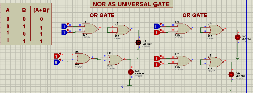
NOR as Universal Gate in Proteus ISIS
In this section, we are going to design the 3 basic logic gates(AND, OR and NOT) using NOR gate. While Designing the circuits, we need the following components:
Material Required
- NOR Gate
- Logic Toggle
- LED
- Ground Terminal
- Connecting Wires
NOT Gate
- In order to design a NOT Gate with NOR Gate, we simply need to combine the inputs.
- Mathematically,
(A.A)'=A'
- The Proteus simulation of NOR gate acting as a NOT gate, is shown in the below figure:
- I have attached an LED at the output to analyze the working.
- Hence, we found the Truth Table as:
OR Gate
During the formation of OR Gate through NOR Gate, we have to keep in mind the following statement:
"The output of NORed inputs is also the ORed input."
We denote this Statement as:
(A.B)'=A+B
- Take two NOR Gates.
- Connect the second NOR Gate's inputs with each other.
- Join the output of first one with the output of the other.
- Join grounded LED and Logic Probes for input and output respectively.
- Pop the play button.
Change the Values of Logic toggles according to the truth table.
Notice that in the formation of current Gate, we implemented the NOT Gate, derived from the NOR Gate that we made before this.
AND Gate
The core statement of the formation of AND Gate through NOR is given next:
"The NORed output of Complements of the input is AND Gate."
Mathematically,
(A'+B')'=AB
- Get the two NOR Gates from Pick Library.
- Fix them vertically at the working sheet.
- Connect the input of each of them with themselves.
- Join Logic Toggle with each of it.
- Take another NOR Gate from the pick Library.
- Connect the output of 1st two with the input of the third.
- Get the Grounded LED and fix it at the remaining output.
- Press the Play sign of the Proteus ISIS.
- Design the Truth Table by applying the required inputs.
[TEPImg9]
Advantages
- It occupies little space.
- It is less expensive.
- we can use it in the place of four Gates.
- It is less complex.
Truss, Today we learnt about the core concepts about the NOR Gate. we saw why we call it as universal Gate and also we saw the Practical experiments to prove our discussion.
XOR Gate with Truth Table in Proteus
Hey pals, we hope you are doing well. In our previous lecture, we discussed the basic DLD Basic Logic Gates and simulated in Proteus. Today, we are going to discuss another logic gate called Exclusive OR Gate(XOR Gate). We will also design the XOR Gate in Proteus using the basic logic gates(i.e. AND, OR and NOT), discussed in the previous lecture.
In today's tutorial, we are going to focus on:
- What are Exclusive OR Gates
- Experimental Proof in Proteus ISIS.
- How Truth Table of Exclusive OR Gate is designed.
- How is its Timing Diagram?
- Circuit of Exclusive OR Gate in Proteus Simulation
- Applications of Exclusive OR Gates
Exclusive OR Gate(XOR Gate)
- In the Exclusive OR Gate(XOR Gate), the output will be HIGH(1), only if the odd no. of inputs is HIGH(1) and at least one of the inputs is LOW. (it's a bit complex, will understand it in the next section)
- The XOR Gate is denoted by a plus sign with a circle around it between
the inputs i.e. .
- XOR gate is designed by combining standard logic gates(i.e. AND, OR and
NOT), but because of its extensive use in arithmetic operations and
error detection, it's considered a standard logic gate.
- The Truth Table of XOR Gate is given below:
| A |
B |
|
| 0 |
0 |
0 |
| 0 |
1 |
1 |
| 1 |
0 |
1 |
| 1 |
1 |
0 |
- The XOR Gate symbol along with its representation and truth table is shown in the below figure:
Working Principle of XOR Gate
Its definition has two conditions in it:
- Odd no. of Inputs should be HIGH
- At least one of the inputs should be LOW
We have seen in the 2-Input XOR truth table, the output is HIGH in the 2nd and 3rd Rows, because these rows are fulfills both conditions i.e., we have an odd no of HIGH inputs(1 input is HIGH) and at least 1 LOW input(1 Input is LOW). While, in the 1st and 4th rows, both conditions are unfulfilled, thus getting LOW at the output.
Now, let's have a look at the truth table of the 3-input XOR Gate:
Image
Now it will get more clear, as you can see in the 4th row, we have 1 HIGH Input and 2 LOW Inputs, thus both conditions are fulfilled and we are getting HIGH at the OUTPUT. But in the 7th row, 2 Inputs are HIGH and 1 is LOW, although the 2nd condition is fulfilled i.e. we have at least 1 LOW input but the first condition is unfulfilled i.e. we have even no of HIGH Inputs. That's why we are getting LOW at the output. I hope now it gets clear.
Mathematical Representation of XOR
Now let's understand the output of the XOR gate mathematically. XOR gate is used in arithmetic calculations because it adds the inputs and gets the carry.
Here's the mathematical calculation of XOR truth table:
0+0=0
0+1=1
1+0=1
1+1=0 (Carry)
Here's the Proteus demonstration of the XOR truth table:
Design XOR Gate with Standard Logic Gates
Now, we are going to design an XOR gate using the basic logic gates i.e. AND, OR and NOT. The formula for XOR Gate is as follows:
Y = A.(B)' + (A)'.B
As you can see in the above equation, we can get an XOR output(Y) by applying 3 logic gates i.e. AND, OR and NOT, on the inputs(A and B).
Let's verify this equation by putting values from the XOR truth table:
For 1st Row:
=0.(0)'+(0)'.0
=0.1+1.0
=0+0
=0
For 2nd Row:
Now, A=0, B=1:
=0.(1)'+(0)'.1
=0.0+1.1
=0+1
=1
For 3rd Row:
Consider A=1, B=0:
=1.(0)'+(1)'.0
=0.1+0.0
=1+0
=1
For 4th Row:
At last, check the expression when A=1, B=1:
=1.(1)'+(1)'.1
=1.0+0.1
=0+0
=0
So, now let's design this equation for the XOR Gate in the Proteus software. Let's get started:
Proteus Simulation of XOR Gate
As we have seen in the previous section, we need to implement this equation in the Proteus software:
Y = A.(B)' + (A)'.B
So, open your Proteus software and get these components from the Proteus library:
Material Required:
- AND Gate
- OR Gate
- NOT Gate
- Logic Toggle
- LED
Circuit Diagram of XOR Gate:
Here's the circuit diagram of the XOR Gate in Proteus using the standard logic gates i.e. AND, OR and NOT:
- As you can see in the above figure, the upper AND gate is implementing the first part of the equation i.e. A.(B)' and the second AND gate is implementing the second part i.e. (A)'.B
- NOT Gate in inversing the inputs, placed at the inputs of AND Gates.
- Finally, we placed an OR gate to add the outputs from both AND gates so that we could complete the equation i.e.
A.(B)' + (A)'.B
- Finally, we placed an LED at the output.
Applications of XOR Gate
XOR Gate is used in many circuits as:
- We use XOR Gate in Half Adder.
- It is used in the circuit of Controlled inverters.
- XOR is also used in comparators.
- Subtractor is the application of XOR Gate.
- The parity checker is made through XOR Gate.
- XOR is used in the Arithmetic Logic Circuits.
- Circuit of Binary to Grey and vice versa.
Today, we discussed the Exclusive OR Gate in detail. We have also designed the simulation of XOR Gate in PRoteus software with the help of basic logic gates i.e. AND, OR and NOT gates. That's all for today. Take care!!!
Introduction to ATmega4809
Hi Guys! I welcome you on board. Happy to see you around. In this post today, I’ll walk you through the Introduction to ATmega4809.
The ATmega4809 is a type of microcontroller that belongs to the megaAVR® 0-series. It features an AVR® processor with a clock speed running at up to 20 MHz. It comes with a Flash memory size up to 48 KB, 256 bytes of EEPROM, and 6 KB of SRAM. It is available in 28-, 32-, 40-, or 48-pin packages.
I suggest you buckle up as I’ll detail the complete Introduction to ATmega4809 covering datasheet, pinout, features, power ratings, and applications.
Let’s get started.
Introduction to ATmega4809
- The ATmega4809 microcontroller belongs to the megaAVR® 0-series that contains an AVR processor.
- The series carries low power features with the latest core independent peripherals.
- The ATmega4809 utilizes Microchip's latest technologies with an efficient and low-power architecture including SleepWalking, Event System, and accurate analog features.
- This device carries Single-pin Unified Program Debug Interface (UPDI) that is a bi-directional single wire interface and needs a programmer that supports UPDI.
- The clock speed is 20MHz which is required for the synchronization of all internal functions.
- The microcontroller program is stored in the flash memory which is around 48KB. While EEPROM and SRAM are 256bytes and 6KB respectively. Write/Erase endurance for flash memory is 10,000 cycles and for EEPROM is 100,000 cycles.
- SRAM memory is used to produce and manipulate variables when this runs. The EEPROM memory is a non-volatile memory that stays stored in the board even when board power is removed.
- There are 4 UART communication protocols and one SPI and one I2C communication protocol are available on the microcontroller.
- The UART is a serial communication protocol that carries two pins Rx and Tx. The Rx is a receiving pin that is used to receive the serial data while Tx is a transmission pin used to transfer serial data.
- I2C is a two-wire communication protocol that carries two pins SDL and SCL. The SDL is a serial data line that carries the data while SCL is a serial clock line that is used for the synchronization of all data transfer over an I2C bus.
- SPI stands for a serial peripheral interface that is mainly used to develop the communication between the controller and other sensors and shift registers. Two pins: MISO (Master Input Slave Output) and MOSI (Master Output Slave Input) are incorporated for SPI communication. These pins are installed to receive or send data by the controller.
- This device comes with three sleep modes: Idle, standby, and power down. The sleep mode is the mode when nothing happens. Simply put, during sleep mode device remains in rest mode. As nothing taking place during the sleep mode, at that point the device consumes the lowest power and the crystal oscillator is turned off.
- The device also offers a power-on-reset (POR) and brown-out-detection (BOD). The power-on-reset just resets the device when the signal is provided to the device.
- The brown-out-detection is a protection circuit that monitors when the supply voltage goes below down a certain level and consequently puts the device into a reset state which leads to proper startup when power is applied back again.
- The controller also contains 16-channel 10-bit ADC and an analog comparator.
- Other features include configurable custom logic, 5x16 bit timer, cyclical redundancy check, watchdog timer, and hardware multiplier.
ATmega4809 Datasheet
Before you incorporate this device into your electrical project, it’s wise to scan through the datasheet of the component that features the main characteristics of the device. Click the link below and download the datasheet of ATmega4809.
Available Packages
ATmega4809 comes in different pin mappings mainly dependent on the current hardware.
48 Pin Package
It is the standard pin package that comes with 9 PWM pins and a flash memory of 48KB. Know that this 48-pin package is only available on ATmega4809 and ATmega3209.
This package comes with 4 UART communication protocols and one SPI protocol.
40 Pin Package
This pinout is almost identical to the 48-pin package with lesser pins and it comes with 8 PWM pins.
This pinout is reserved for ATmega4809 only. Like a 48-pin package, this pinout carries 4 UART and one SPI communication protocol.
32-Pin Package
This pinout is a robust and clean design that comes with 8 PWM pins.
Know that this pinout is not compatible with Arduino shields.
28-Pin Package
This is the 28-pin package that comes with 8 PWM pins and a clock frequency of around 20MHz. Again, this pinout is also not compatible with Arduino shields.
The 28-pin package comes with 3 UART and one SPI communication protocol.
Uno WiFi
The Arduino Uno WiFi Rev2 hardware incorporates this pinout. It comes with 6 PWM pins. Any code written for Arduino UNO WiFi Rev 2 is equally compatible with this pinout. It is important to note that Uno WiFi pinout is only reserved for ATmega3209/4809.
Nano Every
The Arduino Nano Every incorporates this pinout. The code written for Arduino Nano Every can run for this pinout without any modifications. You’ll get this pinout when you select ATmega4809 from the Arduino IDE software.
ATmega4809 Pinout
The following figure shows the pinout diagram of ATmega4809 that comes in a 48-pin package.
ATmega4809 Features
- No. of pins = 48
- Flash memory = 48KB
- SRAM = 6KB
- EEPROM = 256 bytes
- Also includes Hardware multiplier
- Three sleep modes: Idle, Standby, Power Down
- Event System for core independent and predictable inter-peripheral signaling
- Comes with Power-On Reset (POR) and Brown-Out Detection (BOD)
- Contains Single pin programming and debugging interface (UPDI)
- Carries 16 Channel 10-bit ADC with Voltage Reference
- Features Analog Comparator (AC) and Watchdog Timer
- Configurable Custom Logic (CCL) with up to four programmable Look-up Tables (LUT)
- Contains 5x 16-bit Timer (TCA / TCB) and Cyclical Redundancy Check (CRC/SCAN)
- SPI / I2C / USART
- Five selectable internal voltage references: 0.55V, 1.1V, 1.5V, 2.5V, and 4.3V
ATmega4809 Applications
- Employed in high responsive command and control applications.
- Used in embedded systems and real-time control systems.
- Used in industrial automation and home automation.
That’s all for today. I hope you find this article helpful. If you have any questions, you can ask me in the section below. I’d love to help you the best way I can. You are most welcome to share your valuable suggestions and feedback around the content we share so we keep producing quality content based on your exact needs and requirements. Thank you for reading the article.