STM32 SPI Communication

The SPI (Serial Peripheral Interface) protocol, or rather the SPI interface, was originally devised by Motorola (now Freescale) to support their microprocessors and microcontrollers. Unlike the I2C standard designed by Philips, the SPI interface has never been standardized; nevertheless, it has become a de-facto standard. National Semiconductor has developed a variant of the SPI under the name Microwire bus. The lack of official rules has led to the addition of many features and options that must be appropriately selected and set in order to allow proper communication between the various interconnected devices. The SPI interface describes a single Master single Slave communication and is of the synchronous and full-duplex type. The clock is transmitted with a dedicated line (not necessarily synchronous transmission that has a dedicated line for the clock) and it is possible to both transmit and receive data simultaneously. The figure below shows a basic connection diagram between two peripherals that make use of the SPI interface.

From the figure, it is immediately possible to notice what has just been said, namely that the communication generally takes place between a Master and a Slave. The interface presents 4 connection lines (excluding the ground however necessary), for which the standard SPI is also known as 4 Wire Interface. The Master starts the communication and provides the clock to the Slave. The nomenclature of the various lines in the SPI interface is normally as follows:

  • MOSI: Master Output Slave In. Through this line the master sends the data to the selected slave;
  • MISO: Master Input Slave Output. Through this line the slave sends the data to the master;
  • SCLK: Serial Clock is generated by the master device, so it is the master starts the communication and the clock synchronizes the data transfer over the bus. The SPI clock speed is usually several MHz (today up to 100 MHz);
  • SS: Slave Select or CS (Chip Select) generated by the master to choose which slave device it wants to communicate with (it must be set to a low logic level). SS (or CS) is not indispensable in all applications.

In addition to this standard nomenclature, there are other acronyms.

For example:
  • The MOSI line is also called: SDO (Serial Data Out), DO (Data Out), DOUT and SO (Serial Out)
  • The MISO line is also called: SDI (Serial Data In), DI (Data In), DIN and SI (Serial In)
  • The Clock line is also called: CLK, SCK (Serial Clock).
  • The Enable line is also called: CS (Chip Select), CE (Chip Enable)

The first advantage in SPI communication is faster communication, instead, the first disadvantage is the presence of the SS pin necessary to select the slave. It limits the number of slave devices to be connected and considerably increases the number of lines of the master dedicated to SPI communication as the connected slaves increase.

To overcome these problems, the devices in the daisy chain can be connected (output of a device connected to the input of the next device in the chain) as shown in the figure below where a single slave selection line is used.

The disadvantages, however, are the lower updating speed of the individual slaves and signal interruption due to the failure of an element.

We can use this communication to put in communication our micro-controller with different peripherals as Analog-Digital Converters (ADCs), Digital-Analog Converters (DACs), EEPROM memories, sensors, LCD screen, RF module, Real Time Clock, etc.

The STM32 micro-controllers provide up to 6 SPI interfaces based on the type of package that can be quickly configured with STCube Tool.

STCube Tool initializes the peripherals with HAL (Hardware Abstraction Layer) library. The HAL library creates for SPI (as all peripherals) an C structure:

  • struct SPI_HandleTypeDef
It is so defined: Where the main parameters are:
  • Instance: is the pointer variable it describes the SPI that we want to use. If we use SPI1, the name of the instance is SPI1.
  • Init: is an instance that points to the structure ( SPI_InitTypeDef) used to initialize the device. We will discuss the structure SPI_InitTypeDef shortly.
  • pTxBuffPtr, pRxBuffPtr: are pointer variables that point to an internal buffer. They are used to store the data during the communication when the programmer handles the SPI in interrupt mode (we will see forward)
  • hdmatx, hdmarx: are the pointer variable to instances of the DMA_HandleTypeDef struct. They are used when the programmer handles the SPI in DMA mode (will see forward).

As just said to initialize the SPI peripheral to be used, it is necessary to use the struct SPI_InitTypeDef. It is defined as follow:

When we use the STcubeMX to initialize the SPI peripheral we are modifying this structure

In details:
  • Mode specifies the SPI operating mode, and Direction specifies the SPI bidirectional mode state. It is very easy to configure in STCubeMx. If we want to configure the SPI1. We can find SPI windows in Pinout&Configuration -> Connectivity. Here we can select between the SPI available. Now is possible to select the communication mode (Master, Slave, half-duplex, full-duplex, etc.) as follow:

If the slave supports, the full-duplex communication can be enabled.

  • DataSize indicates the SPI data size. The user can select 8bit or 16bit.
  • CLKPolarity defines if the serial clock steady state is LOW or HIGH.
  • CLKPhase defines if the bit capture (trigger) takes place when the clock is on the falling edge or rising edge.
  • NSS: if selected "Output Hardware" the slave select signal is managed by hardware otherwise is managed by software using the SSI bit.
  • BaudRatePrescaler can be select the Baud Rate prescaler value.
  • FirstBit indicates if data transfers start from Most Significant Bit (MSB) or Last Significant Bit (LSB).
  • TIMode specifies if the TI mode is enabled or not.
  • CRCCalculation: to enable to activate the CRC calculation.
  • CRCLength: to define the length of CRC data.
  • CRCPolynomial specifies the polynomial (X0+X1+X2) used for the CRC calculation. This parameter is an odd number 1 and 65535.

By enabling the SPI and the chip select pin, the pins available on the microcontroller are automatically chosen to manage this interface (but they can be changed by looking for the alternative functions of the different pins of the microcontroller). For example, in our case the following pins are selected:

  • PA4 SP1_NSS
  • PA5 SP1_SCK
  • PA6 SP1_MISO
  • PA7 SP1_MOSI

Now you can generate the initialization code. Before being able to write the first code to manage this communication interface, it is necessary to understand the functions that the libraries provide and the different communication modes.

As for other communication interfaces, the HAL library provides three modes to communicate: polling mode, interrupt mode, and DMA mode.

Where To Buy?
No.ComponentsDistributorLink To Buy
1STM32 NucleoAmazonBuy Now

STM32 SPI Communication in Polling Mode

Using the SPI in Polling Mode is the easiest way, but it is the least efficient way as the CPU will remain in a waiting state for a long time. HAL library provides the following functions to transmit and receive in polling mode:

  • HAL_SPI_Receive(SPI_HandleTypeDef *hspi, uint8_t *pData, uint16_t Size, uint32_t Timeout)

Master receives data packets in blocking mode (polling mode).

The parameters are:

  • hspi is a pointer to a “SPI_HandleTypeDef” structure. “SPI_HandleTypeDef” structure includes the configuration information for SPI module.
  • pData is a pointer to data buffer
  • Size is the amount of data to be sent
  • Timeout is the timeout duration
  • HAL_SPI_Transmit(SPI_HandleTypeDef *hspi, uint8_t *pData, uint16_t Size, uint32_t Timeout)

Master transmits data packets in blocking mode (polling mode).

If the slave device supports, the full-duplex mode:

  • HAL_SPI_TransmitReceive(SPI_HandleTypeDef *hspi, uint8_t *pTxData, uint8_t *pRxData, uint16_t Size, uint32_t Timeout)

Master transmits and receives data packets in blocking mode (polling mode).

The parameters are:

  • hspi is a pointer to a “SPI_HandleTypeDef” structure. “SPI_HandleTypeDef” structure includes the configuration information for SPI module
  • pTxData is a pointer to transmission data buffer
  • PRxData is a pointer to reception data buffer
  • Size is the amount of data to be sent
  • Timeout is the timeout duration

STM32 SPI Protocol in Interrupt Mode

Using the SPI in Interrupt Mode, also called non-blocking mode. In this way, the communication can be made more effective by enabling the interrupts of the SPI in order to receive, for example, signals when the data has been sent or received. This improves CPU time management. In applications where all the management must be deterministic and it is not known when an interrupt can arrive, these can potentially manage the time management of the CPU, especially when working with very fast buses such as SPI. We can enable the SPI interrupts directly during the initialization with STCube Mx.

HAL library provides the following functions to transmit and receive in interrupt mode:

  • HAL_SPI_Receive_IT(SPI_HandleTypeDef *hspi, uint8_t *pData, uint16_t Size)
Master receives data packets in non-blocking mode (interrupt mode). The parameters are:
  • hspi is a pointer to a “SPI_HandleTypeDef” structure. “SPI_HandleTypeDef” structure includes the configuration information for SPI module
  • pData is a pointer to data buffer
  • Size is the amount of data to be sent
To handle the interrupt needs to write our code in the callback:
void HAL_SPI_RxCpltCallback(SPI_HandleTypeDef * hspi) { // Message received .. Do Something ... }
  • HAL_SPI_Transmit_IT(SPI_HandleTypeDef *hspi, uint8_t *pData, uint16_t Size)

Master transmits data packets in blocking mode (interrupt mode).

To handle the interrupt needs to write our code in the callback:

void HAL_SPI_TxCpltCallback(SPI_HandleTypeDef * hspi) { // Message transmitted.... Do Something ... }

If the slave device supports, the full-duplex mode:

  • HAL_SPI_TransmitReceive_IT(SPI_HandleTypeDef *hspi, uint8_t *pTxData, uint8_t *pRxData, uint16_t Size)

Master transmits and receives data packets in non-blocking mode (interrupt mode).

To handle the interrupt needs to write our code in the callback:

void HAL_SPI_TxRxCpltCallback(SPI_HandleTypeDef * hspi) { // Message transmitted or received.. .. Do Something ... }

STM32 SPI Communication in DMA Mode

Using the SPI in DMA Mode the SPI bus can be used at its maximum speed, in fact, since the SPI must store the received and transmitted data in the buffer to avoid overloading it is necessary to implement the DMA. In addition, use by DMA mode frees the CPU from performing "device-to-memory" data transfers. We can easily configure the DMA during the initialization using STCubeMx :

In this case, the DMA is enabled in normal (we can use it in circular mode) mode both in transmission and reception

HAL library provides the following functions to transmit and receive in DMA mode:

  • HAL_SPI_Receive_DMA(SPI_HandleTypeDef *hspi, uint8_t *pData, uint16_t Size)

Master receives data packets in non-blocking mode (DMA mode).

The SPI device receives all bytes of data in the buffer one by one until the end in DMA mode. At this point, the callback function will be called and executed where something can be done.

void HAL_SPI_RxCpltCallback(SPI_HandleTypeDef * hspi) { // Message received .. Do Something ... }
  • HAL_SPI_Transmit_DMA(SPI_HandleTypeDef *hspi, uint8_t *pData, uint16_t Size)

Master transmits data packets in non-blocking mode (DMA mode).

The SPI device sends all bytes of data in the buffer one by one until the end in DMA mode. At this point, the callback function will be called and executed where something can be done.

void HAL_SPI_TxCpltCallback(SPI_HandleTypeDef * hspi) { // Message transmitted….. Do Something ... }

If the slave device supports, the full-duplex mode:

  • HAL_SPI_TransmitReceive_DMA(SPI_HandleTypeDef *hspi, uint8_t *pTxData, uint8_t *pRxData, uint16_t Size,)

Master transmits and receives data packets in non-blocking mode (DMA mode).

The SPI device sends or receives all bytes of data in the buffer one by one until the end in DMA mode. At this point, the callback function will be called and executed where something can be done.

void HAL_SPI_TxRxCpltCallback(SPI_HandleTypeDef * hspi) { // Message transmitted or received.... Do Something ... }

We are now ready to handle an SPI communication with STM32.

Write and Read an I2C EEPROM with STM32

EEPROMs (Electrically Erasable Programmable Read-Only Memories) allow the non-volatile storage of application data or the storage of small amounts of data in the event of a power failure. Using external memories that allow you to add storage capacity for all those applications that require data recording. We can choose many types of memories depending on the type of interface and their capacity.

EEPROMs are generally classified and identified based on the type of serial bus they use. The first two digits of the code identify the serial bus used:

  • Parallel: 28 (for example 28C512) much used in the past but now too large due to having many dedicated pins for parallel transmission
  • Serial I2C: 24 (for example 24LC256)
  • Serial SPI: 25 (for example 25AA080A)
  • Serial - Microwire: 93 (for example 93C56C-E/SN)
  • Serial – UN I/O: 11 (for example 11LC040-I/SN)

Now we will see how to write or read data on an I2C EEPROM like 24C256C. This serial EEPROM is organized as 32,768 words of 8 bits each. The device’s cascading feature allows up to eight devices to share a common 2-wire bus. It is available in various 8-pin packages

The device can be used in applications consuming low power. The device is available in all standard 8-pin packages. The operating voltage is comprised of between 1.7V and 5.5V.

  • Serial Clock (SCL) is an input pin used to control data flow. On the positive-edge clock, the data is inserted into the EEPROM device, while on the negative edge clock, the data is processed out of the EEPROM module.
  • Serial Data (SDA) is a bidirectional input-output for serial data transfer. It is an open-drain pin.
  • Device Addresses (A2, A1, A0) are input pins to set the device address. These pins allow you to customize the address of the device within the I2C bus. They must connect directly to GND or to VCC (hard wired). If these pins are left floating, the A2, A1, and A0 pins will be internally pulled down to GND. When using a pull-up resistor, it recommends using 10kOhm or less.
  • Write Protect (WP) is an input pin. We can perform normal writing operations, by connecting it to GND; When connected directly to VCC, all write operations to the memory are restricted. If this pin is left open/floating, it will be pulled down to the GND(internally). When using a pull-up resistor, it recommends using 10kOhm or less.
  • Device Power Supply (VCC)
  • Ground (GND)

In our example, we connect A0, A1, A2 directly to VCC in this way the device address is 1010111 (in general A0, A1, A2 identify the last three significant bits of the device address 1 0 1 0 A2 A1 A0) is 0x57 in Hexadecimal. The 4 most significant bits are preset (Control Code), the A0, A1, A2 are Chip Select Bits.

Now we start with our project using STNucleoL053R8 and STCube to generate the initialization code. Below is shown the connection

  • A0, A1, A2 are connected directly to VCC in this way the device address is 1010111 (in general A0, A1, A2 identify the last three significant bits of the device address 1 0 1 0 A2 A1 A0) is 0x57 in Hexadecimal.
  • WP is connected to the ground to allow the normal write operation
  • SCL and SDA are connected to PA8 and PA9 respectively of STM32L053R8

So, we configure the I2C1 using STCube and leave all configuration as it is and we will operate in polling mode.

In GPIO setting select PA9 (SDA) and PA8 (SCL).

Now we create a new STM32CubeMX project with the following steps:
  • Select File > New project from the main menu bar. This opens the New Project window.
  • Go to the Board selector tab and filter on STM32L0 Series.
  • Select NUCLEO-L053R8 and click OK to load the board within the STM32CubeMX user interface
      Then the tool will open the pinout view.
  • Select Debug Serial Wire under SYS, for do it click on System Core (on the topo right) and then select SYS and finally flag on “Debug Serial Wire”.
 
  • Select Internal Clock as clock source under TIM2 peripheral. To do this click on Timers and then select TIM2. Now go to clock source and select through the drop-down menu “internal clock”.
  • Select and enable in “Connectivity” the I2C1 and left all configuration as it is and we will operate in polling mode.
  • Configure in GPIO setting PA9 (SDA) and PA8 (SCL) to manage the I2C communication.
  • Check that the signals are properly assigned on pins:
    • SYS_SWDIO on PA13
    • TCK on PA14
    • SDA I2C1on PA9
    • SCL I2C1on PA8
  • Go to the Clock Configuration tab and no change the configuration in order to use the MSI as input clock and an HCLK of 2.097 MHz.
  • Select Timers -> TIM2 and change the Prescaler to 16000 and the Counter Period to 1000.
  • In the Project Manager tab, configure the code to be generated and click OK to generate the code.

Our project has been initialized by STCubeMX. In the /Core/Src/main.c we will find our main where we will write the main body of our program.

Now let’s see what the code generator did:

First of all, we find the “Include” section we can add the library needed.

 
/* USER CODE END Header */ /* Includes ------------------------------------------------------------------*/ #include "main.h"
In our case we can add also “stm32l0xx_hal.h” library to be able to use HAL library (I2C HAL library included)
#include "stm32l0xx_hal.h " #include "Var.h " #include "Funct.h "
In “Private variables” has been defined two privates variable htim2 and hi2c1;
  • - htim2 as first parameter an instance of the C struct TIM_HandleTypeDef;
  • - hi2c1 as first parameter an instance of the C struct UART_HandleTypeDef.
/* Private variables ---------------------------------------------------------*/ TIM_HandleTypeDef htim2; UART_HandleTypeDef hi2c1; unsigned short int address; // eeprom address unsigned char EEP_pag = 0x00 // EEPROM page unsigned char EEP_pos = 0x00 // EEPROM position unsigned char rdata = 0x00 // to store the data read from EEPROM
In “Private function prototypes” we find the protype of function to initialize the System Clock, GPIO, timer and peripheral:
/* Private function prototypes -----------------------------------------------*/ void SystemClock_Config(void); static void MX_GPIO_Init(void); static void MX_TIM2_Init(void); static void MX_I2C1_Init(void);

This function has been generated automatically by STCubeMx with the parameter selected.

The main contains the initialization of the peripherals and variables, before the while loop the code call the function Write_EEPROM() and Read_EEPROM() to write and read a data in a specific address of the EEPROM. these functions were written in EEPROM.c, a C file added to our project in the src folder.

  int main(void) { /* USER CODE BEGIN 1 */ /* USER CODE END 1 */ /* MCU Configuration--------------------------------------------------------*/ /* Reset of all peripherals, Initializes the Flash interface and the Systick. */ HAL_Init(); /* USER CODE BEGIN Init */ /* USER CODE END Init */ /* Configure the system clock */ SystemClock_Config(); /* USER CODE BEGIN SysInit */ /* USER CODE END SysInit */ /* Initialize all configured peripherals */ MX_GPIO_Init(); MX_TIM2_Init(); MX_I2C1_Init();   /* USER CODE BEGIN 2 */ address = 0x00 << 8 | 0x00 // eeprom page 0 , position 0 // Now we want to store 10 in page 0x00 and position 0x00 of EEPROM Write_EEPROM(address, 10, 0) // Now we want store in rdata variable the content of cell memory 0x0000 rdata = Read_EEPROM(address, 0)   /* USER CODE END 2 */   /* Infinite loop */ /* USER CODE BEGIN WHILE */ while (1) { /* USER CODE END WHILE */ } /* USER CODE BEGIN 3 */ } /* USER CODE END 3 */ }
Furthermore, we have added two header files and one c file:
  • Var.h contains the declaration of global variables:
/** Var.h * Created on: 27 ott 2021 * Author: utente */ #ifndef INC_VAR_H_ #define INC_VAR_H_ extern unsigned char buf[20]; extern int i; #endif /* INC_VAR_H_ */
  • Funct.h contains the prototype of the user function
/** Funct.h * Created on: 28 ott 2021 * Author: utente */ #ifndef INC_FUNCT_H_ #define INC_FUNCT_H_ extern unsigned char Read_EEPROM(unsigned int, unsigned char); extern void Write_EEPROM(unsigned int, unsigned char, unsigned char); #endif /* INC_FUNCT_H_ */
  • EEPROM.c contains the function written by the user to handle the writing and reading operation with EEPROM:
  • unsigned char Read_EEPROM(addr, device) reads from cell memory address (addr)and store the content in dato.
  • void Write_EEPROM(addr, dato, device) writes data (dato) to memory address (addr).
/** Serial.c * Created on: Oct 29, 2021 * Author: utente */ #include "stm32l0xx.h" // Device header #include "stm32l0xx_hal_conf.h" #include "stm32l0xx_hal.h " #include "Var.h " #include "Funct.h " extern I2C_HandleTypeDef hi2c1; unsigned char Read_EEPROM(unsigned int addr, unsigned char device) { unsigned char page; uint8_t dato; page=0xAF; // due to chip select bits setting HAL_I2C_Mem_Read(&hi2c1,page, addr, I2C_MEMADD_SIZE_16BIT, &dato,1,5); return dato; } void Write_EEPROM(unsigned int addr, unsigned char dato, unsigned char device) { unsigned char page; page=0xAF; //due to chip select bits setting HAL_I2C_Mem_Write(&hi2c1,page, addr, I2C_MEMADD_SIZE_16BIT, &dato,1,5 ); while(HAL_I2C_IsDeviceReady(&hi2c1, 0xA0, 1, HAL_MAX_DELAY) != HAL_OK); HAL_Delay(10); }
Now we are ready to compile and run the project:
  1. Compile the project within IDE.
  1. Download it to the board.
  2. Run the program.
So, that was all for today. I hope you have enjoyed today's lecture. In the next tutorial, we will have a look at How to perform SPI Communication with STM32. Till then take care and have fun !!! :)

Designing Logic Gates in PLC Simulator

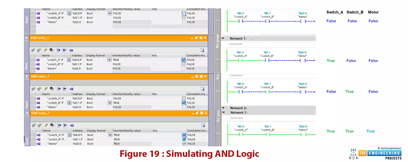
Hello friends, I hope you all are doing great. In today's tutorial, we are going to design logic gates in PLC Simulator. It's our 4th tutorial in Ladder Logic Programming Series. We come today to elaborate the logic gates with comprehensive details for their importance in PLC programming. you can consider logic gates as the building blocks of ladder logic programming. Like every time we start with telling what you guys are going to have after completing this session? For those who like to buy their time and calculate for feasibility, I’d like to say by completing this article, you are going to know everything about what types of logic gates, how they are designed and how they work, how you can translate the logic in your head into the logic gate and some about logic calculation which is so-called logic algebra, and for sure the connection with examples between logic gates and the Ladder logic programming. In our previous tutorial, we have Created First Project using Ladder Logic, where we designed a simple logic by using contact and coil. Today, we are going to extend that code and will design different logic gates in ladder logic.

We are discussing these logic gates because they are the main building block of complicated logic. Normally, complex logic is designed using multiple logic gates. So, today, we will simulate the basic logic gates i.e. AND, OR, and NOT, while in the next lecture, we will simulate NAND, NOR, XOR and XNOR in PLC Simulator. So, let's get started:

Logic gates

In very simple language, it is a Boolean decision that has one of only two values either “TRUE” or “FALSE”, not both. For instance, the decision to run or shut down a motor, open or close a valve etc. Well! For deciding such Boolean nature thing, there are two things, inputs and logic to apply on those inputs. On the other way, logic gates apply some sort of logic to the inputs to determine the state of the output.

Truth table

It’s a table that lists all possible combinations of the inputs and the state of the output for each record. For example, a gate with two inputs has four possible combinations of the inputs and four states of the output. inputs.

Basics of logic gate

There are seven basic logic gates. Some of them have only one input while others have two inputs. There are seven basic logic gates which are “AND”, “OR”, “NOT”, “NOR”, “XOR”, “XNOR”, and “NAND”. So let us enjoy a short journey with them having a fast stop at each one’s station. Our trip will include, how they work, design, timing diagram, and connection with ladder logic programming.

Simulating ANR, OR, and NOT logic

  • The AND, OR, and NOT logic are considered the basic building block logic for designing the complicated logic to decide the output status.
  • By using two switches A and B and one output representing lamp or MOTOR, we can design and program these logics and simulate them on the PLCSIM simulator.
  • Table 1 lists the truth table of the three logic AND, OR, and NOT.

Table 1: Truth table of the AND, OR, NOT logic

Switch A Switch B Motor
AND LOGIC
0 0 0
1 0 0
0 1 0
1 1 1
OR LOGIC
0 0 0
0 1 1
1 0 1
1 1 1
NOT LOGIC
Switch Output
0 1
1 0

The “AND” Logic Gate

The “AND” logic gate has two inputs and one output. Like its name, the only condition for having the output become true, is by having both inputs, input A and input B are true. Table 1 lists the truth table of the “AND” gate and Fig. 1 images the symbol of the “AND” gate. In addition, Fig. 2 shows a sample of ladder logic rung that uses “AND” gate logic. It decides the status of the motor based on two switches. The two switches must be in true status for running the motor. ‘to sum up, the logic of the “AND” gate, is that, the output comes to true when and only when both inputs A and B are true.

Table 1: the truth table of “AND” logic gate

Input A Input B Output
False False False
True False False
False True False
True True True

Fig. 1: symbol of “AND” logic gate [1]

In the ladder logic rung shown in Fig. 2, there are two contacts I1 and I2, they are of normally open (NO) type, these two contacts are connected in series, so the only way to set the output to true is that both contacts I1 and I2 must set to true. For full imagination, please notice the timing diagram of the inputs and output signals shown in Fig. 3. It shows the output is only high when both inputs are high.

Fig. 2: sample ladder logic rung for “AND” logic [2]

Fig. 3: The timing diagram of the “AND” logic gate

AND logic in PLC simulator

  • Let us once more enjoy learning further by validating and practicing on the simulator, here you can see in figure 19, on the right the AND logic has been programmed by connecting two switches A and B in series.
  • The motor status is the result of the AND logic between the two switches.
  • On the left, you can see the results of the simulation by setting the status of switches to simulate all truth table conditions and see the motor status changed accordingly.
  • In addition, you can see the truth table of the AND logic on the most right of the figure. So you can review and validate what is going on in the simulator.

Figure 19: Simulating AND logic

The “OR” Logic Gate

This logic gate has two inputs and one output like the “AND” gate. Like its name, the output comes true when either input A or input B comes true as shown in Fig. 4.

Fig. 4: The symbol of “OR” logic gate [1]

Table 2 lists the truth table of the “OR” gate. It lists all possible combinations of inputs and the output status as well. It shows that the output comes to true when input A or input B comes to true.

Table 2: The truth table of the “OR” gate

Input A Input B Output
False False False
True False True
False True True
True True True
 

Figure 5 shows an example of a ladder logic rung that implements the “OR” logic. We can implement this by connecting two inputs I1 and I2 in parallel branches and to the output. like this way of connection, the output can be set to true by simply setting I1 or I2 or both true. Once more, let us see the timing diagram in fig. 6, it is clearly shown that the output goes high as long as either one or both of the inputs are true.

Fig. 5: sample ladder logic rung for “OR” logic [2]

Fig. 6: the timing diagram of the “OR” logic gate

OR logic in PLC Simulator

  • You can see in figure 20, on the right the OR logic has been established and programmed by connecting two switches A and B in parallel.
  • The motor status is the result of the OR logic between the two switches.
  • On the left, you can see the results of the simulation by setting the status of switches to simulate all truth table conditions of the OR logic and see the motor status charged accordingly.
  • In addition, you can see the truth table on the most right of the figure. So you can review and validate what is going on in the simulator.

Figure 20: Simulating OR logic

The “NOT” logic gate

This logic gate has only one input and one output. In a very simple language, the output is the invert logic of the input. So when the input is true, the output would come to false and vise versa as shown in Fig. 7.

Fig. 7: The symbol of the “NOT” logic gate [1]

Table 3 lists the truth table rows of all possible combination of input and output.

Table 3: the truth table of the “NOT” logic gate

Input Output
True False
False True
 

Figure 8 depicts a very simple example of a ladder logic rung that shows the output Q1 is the reverse logic of the input I1. In addition, Fig. 9 shows the timing diagram of input and output of the “NOT” logic gate. It shows clearly that, the output is the reverse of the input.

Fig. 8: Sample of the ladder logic rung representing “NOT” logic [2]

Fig. 9: The timing diagram of the NOT logic gate

Before going further with the logic gates, I want to let you know the good news that, you can implement any logic by using the aforementioned three logic gates “AND”, “OR”, and “NOT”. However, for simplification, the other logic gates are designed based on using these three logic gates in different topologies to perform a specific logic functions.

Not logic in PLC Simulator

  • Also, the NOT logic is one of the primary logic functions, you can see in figure 21, on the right the NOT logic has been designed and programmed by connecting switches A in negative logic in series with the motor.
  • The motor status is the result of the NOT logic of switch A. On the left, you can see the results of the simulation by setting the status of the switch to simulate the two-state of the NOT logic truth table and see the motor status charged accordingly.
  • In addition, you can see the truth table on the most right of the figure. So you can review and validate what is going on in the simulator.

Figure 21: simulating Not logic

Now! I appreciate your follow-up to our PLC tutorial. I am very happy to feel that, by moving further in our plc tutorial our experience is getting increasing bit by bit. However, some questions may come to our mind like does the operator needs to keep pressing input like the push button to keep the motor running? What happens if he released it, does the motor stop? Well! By asking such questions, I can affirm you start your way to master PLC programming and its logic. And let me say the answer to your questions is yes the operator needs to keep pressing the input push-button until the motor has done its task. But that is not the best practice in the real life. There are other techniques to keep the motor running by one touch of the push button, thanks to latching, setting, and resetting techniques as we will show you in the next sections.

Latching output

  • Figure 22 depicts the latching technique that we simply use to keep the motor running by pressing the input push button and having it keep running even after releasing the button.
  • As you can see, I have used the Output as a Virtual Input and placed it in parallel with actual input.
Figure 22: Latching output
  • Table 2 lists the First three scan cycles to show the sequence of operations and how the latching process works when someone will press the Input.
  • In the first scan cycle, when the input gets HIGH, the plc will scan the input "Run (I0.0)" and will find it pressed/ON and thus will make the output "Motor (Q0.0)" HIGH.
  • In the second scan cycle, the input "Run (I0.0)" turned off after being released, but the motor contact is still ON from the previous scan cycle.
  • So, the compiler won't change the status of the OUTPUT and we can say it's latching the output.

Table 2: The first three scan cycles of latching operation

Scan cycle Run (I0.0) Motor status (Q0.0) Motor coil (Q0.0)
1 1 0 1
2 0 1 1
3 0 1 1
  • Now let’s add a way to terminate the latching and stop the motor as per request.
  • Well! Simply figure 23 shows a stop button is added for terminating the latching condition.
  • So in table 2, the RLO for letting the motor running will be unfulfilled by hitting the stop push button in the third scan cycle.
Figure 23: latching with stop button

Simulation of the latching in ladder logic

We may be sure of the logic we wrote for coding the ladder logic of the latching technique. However, at this point how about going to the simulation lab to work out our latch ladder logic program to enjoy validating our ladder code by putting it in the simulator and see how far it match what it is designed for.

Latching Ladder code simulation

  • Now let’s try our latching ladder program in the PLCSIM simulator, by entering our ladder logic and starting the simulator.
  • Figure 24 shows the first four scan cycles. Notice on the left we can set the inputs on and off and see the effects on the right part.
  • In the first scan, every single input and output is at its initial state, so the output is not energized.
  • In the next scan cycle, you can notice we switch on input at I0.0 which is the start push button.
  • Therefore, the motor has been started and running. In the third scan cycle, the start button is switched back off.
  • However, the motor still runs thanks to the latching technique. WOW, we can see our logic is working as we designed for.
  • In the last scan cycle, we tried to test stop latching by hitting the stop pushbutton and indeed it stopped latching and the motor stop running.

Figure 24: simulation result of the first ladder program

We will concentrate on moving forward with ladder coding which is our target. However, we just tried to show you at any time you can validate your ladder at any point to enjoy and confirm you are on the right track as long as you are working on your project.

Latching using set and reset

Let’s use another approach for latching which is based on using set and reset coil. Figure 25 shows the set and reset methods.

  • By hitting set_valve at address I0.2, the valve at Q0.0 will be set ON until a reset command is present by hitting the reset_valve pushbutton at I0.3.
  • It is very easy but you need to take extra care while using set and reset as the last set/reset command will overwrite the previous commands.
  • But wait, what’s if an operator keeps pressing the rest or set button for a long time or if the pushbuttons are the stuck and same thing for the stop button.

Well! The rational expectation is that the motor won’t be able to start. However, the good thing is there is a magic solution to differentiate between the situation of this is a normal stop request by the operator or the button is hold pressed unintentionally or due to an issue with the switches. The one-shot technique can magically recognize the event of pressing or releasing the pushbuttons. Therefore, when it is held for a long time or forever that is only one button press event and for triggering it needs to release and pressed once again. That’s amazing but how does it work? Well! Let’s go demonstrate the concept of how it works, implementation using ladder logic, and give an example to understand it consistently and enjoy the magic of one-shot action.

Figure 25: set and reset for easy latching output

The signal edges

Two edges happened when a pushbutton pressed and released which are falling edge and rising edge as shown in figure 26. It depicts the rising edge when the button is pressed and the falling edge when it has been released. Now, let's move to ladder logic, there are two equivalent rising and falling edge contacts that can be used to tell the PLC this is a one-shot signal. Figure 27 shows how the use of the rising edge of the reset pushbutton |P| at address I0.3. it shows that despite the reset being pressed, its effect in the moment of pressing and then it needs to be released and pressed again to reset the valve at Q0.1. in the next section, let’s get to business and work out one practical example which represents a real problem in the industry just to harvest the fruit of what we have learned so far.

Figure 26: The rising and falling edge [2]

Figure 27: The effects of one-shot technique in ladder logic

So, that was all for today. I hope you have enjoyed today's lecture. In the next tutorial, we will simulate Advance Logic Gates using Ladder Logic Programming. We will design NAND, NOR, XOR and XNOR gates in the next lecture. Thanks for reading.

Creating the First Ladder Logic Program in PLC Simulator

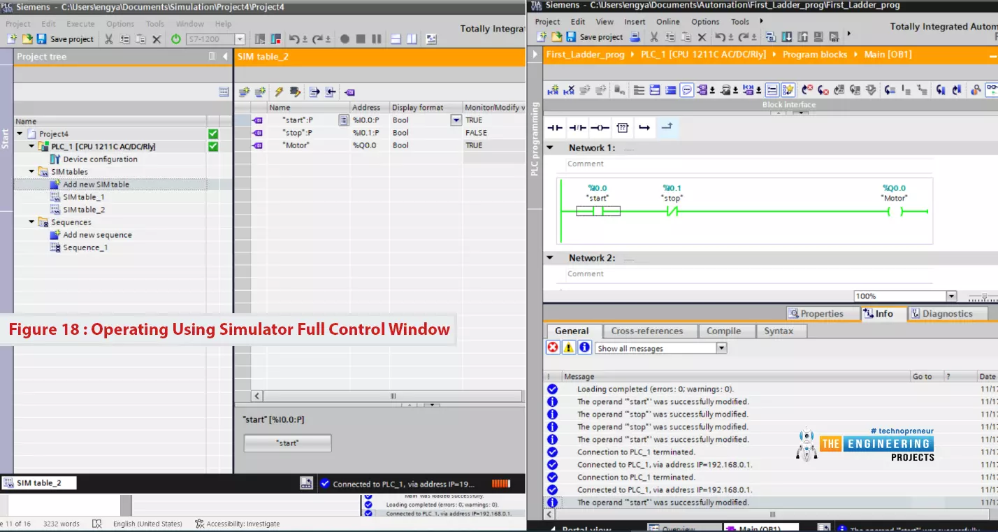
Hello friends, I hope you all are doing great. In today's tutorial, I am going to create the first Ladder Logic Program in PLC Simulator. It's 3rd tutorial in our Ladder Logic Programming Series. In our previous tutorial, we have installed PLC Simulator and now we can say our lab is ready to learn and practice. So let us get to work and get familiar with the ladder logic components.

After this article, you will have a complete understanding of PLC contact and coil including their types and possible causes. Because they are the building block of any rung of a ladder logic program. So let us start with ladder logic rung components.

Ladder Logic Contact/Input

  • In ladder logic programming, a contact represents the input of the system and it could be a button press by the operator or a signal from the sensor.
  • Examples of contacts are toggle switches, pushbuttons, limit switches, sensors like level, pressure, proximity switches et cetera.
  • There are two types of contacts normally used, which are:
    1. Normally Open Contact.
    2. Normally Closed Contact.

1. Normally Open Contact

  • A normally open contact is Open/LOW by default and it gets Closed/HIGH by pressing or getting signal from any external source i.e. sensors.
  • As shown in the first row of figure 1, the contact is open or disconnected by default and then the operator turns it to closed or connected status, shown in the second row.

Figure 1: Normally Open (NO) contact [1]

  • Let's understand it with its equivalent electrical circuit, imagine you wire a switch in series to a lamp as in figure 2.
  • After you complete wiring and connect L1 to the hotline and L2 to the neutral.
  • See that at the start the lamp is off until you come and press the pushbutton then it is turned on.
  • So, here the switch is acting as a normally open switch.

Figure 2: Normally open contact or switch in a circuit [2]


2. Normally Closed Contact

  • A normally closed contact is at HIGH/Closed state by default and gets Low/Open if pressed by the operator.
  • Figure 3 shows the symbol of normally close contact.
  • So it flows current at the very beginning and disconnects the current flow by being pressed by the operator to become like an open circuit or contact.

Figure 3: Normally Closed (NC) contact

  • For elaborating the behavior, let us wire a circuit that is depicted in figure 4.
  • The contact is connected in series with a lamp to convey the current and let it turn on.
  • So initially, the lamp started in ON status when the contact is not activated by the user.
  • And, when the operator activates the contact it turns off.
  • So, the switch is acting as a normally closed switch.

Figure 4: Normally close contact or switch in a circuit [2]


Ladder Logic Coil/Output

  • The coil in ladder logic represents the actuator or the equipment we aim to turn on or off.
  • A good example of a coil is a lamp and motor.
  • Typically it is located at the most right side of the ladder logic rung.
  • Same as contact has two types based on the initial state and the next state after user activation, also the coil comes in two forms which are:
    1. Normally Active Coil
    2. Normally Inactive Coil as shown in figure 5.
  • An inactive coil is normally not energized until it gets connected by connecting the left side to the hot wire thanks to a contact.
  • In contrast, active or negated coil type comes initially On status or energized and turned off when the left side is connected to the hot wire.

Figure 6: active and inactive coil


Create First Ladder Logic program

To our fortune we no longer need wires and devices to practice what we have been learning together, thanks to the simulator, which we have installed in the previous lecture. Let's create a new project on TIA portal software and test it with the PLCSIM simulator.

Creating a new project on TIA Portal

As this is the first time to use our software to write and simulate a ladder logic code, let us go step by step creating our very first project on the TIA portal software.

  • You now get in the Lab by opening the TIA portal and hitting create a new project as shown in Figure 7.
  • On the right, you just need to name your project like “new project” and you may leave the default location of projects or alter the data to the project file location as you prefer.

Figure 7: Creating a new project on TIA portal software

  • You will have to select a PLC controller whom we are going to use. So you simply select one PLC controller as shown in figure 8 and click okay.

Figure 8: adding PLC controller

  • The wizard now goes on asking you to add a program block.
  • You can see in Figure 9, the default program block is the Main block which has the main program and other blocks are additional blocks.
  • So for now let us go with the essential requirements for our program which is the main block and you just double click on the Main block to go to the next step.

Figure 9: adding program block

I just want to say well done! And congratulate you that you are now all set to start writing your first ladder logic rung as shown in Figure 10. It shows on the left the project components including hardware i.e. devices and controllers, networking devices, configurations, program blocks etc. The most important thing you need to know for now is the program blocks which contain the only main block and other blocks as the project needs. Now! please stare your eye toward the right to see the icon bar that contains every ladder symbol. You can see the contact of normally open and normally closed. Furthermore, you should see the coil and more which we are going to go into detail later in our upcoming articles of PLC tutorial.

Figure 10: starting writing ladder code

Writing First program on the TIA Portal

  • WOW! You are a superb learner as I can see you can follow figure 11 and by dragging a contact and dropping it on the blue line, you added a start button of normally open (NO) contact type.
  • For identifying contacts and coils, the compiler assigns a unique name & address to each component and can recognize it anywhere in the program.
  • Therefore, you just set the address and name for every component you add to your rung.
  • The address of components has a specific format that is very logical and easy to understand.
  • For example, the contact address “I0.0”, the first character is “I” which denotes input and it is followed by the number of the input module in the rack that holds all inputs and outputs modules.
  • Then a number of the input channel as each input module has many channels.
  • For instance, an eight channels input module can have numbers from 0 to 7 while 16 channels input module can have numbers from 0 to 15.
  • A period is used to separate between the number of input modules and the channel number.
  • So by set address I0.0, this refers to the very first channel in the first input module in a PLC rack.
  • In addition, a name is used as a tag to easily identify the input i.e. “start” to refer to a start switch.
  • Similarly, you add a stop button of the type normally closed (NC) with address I0.1 which means the second input channel in the first input module.
  • Furthermore, you double-clicked the coil for the motor and set address Q0.0 which means the first output channel in the first module.
  • I know you wonder what is “Q”? Yes! “Q for denoting output like “I” is denoting an input. Well done!. Now let us enjoy simulating the very first code you just have done yourself.

Figure 11: writing the first ladder logic program


Compiling Ladder Logic Program

  • Like any programming language, the first thing to do after writing a program is to compile, to make sure it is free of error and ready to be downloaded into the PLC controller to run.
  • Figure 12 shows the very simple steps to compile your program by clicking the compile icon in the toolbar which is highlighted in yellow.
  • And you can notice in the lowest window below the results of compilation in blue showing that the code is free of error and warnings.

Figure 12: compiling ladder logic program

  • To let you imagine how the compiler can help you to find the error location and type, we have done one mistake in the code and compiled as shown in figure 13.
  • You can notice that compiler is telling the rung that has the issue which is network 1.
  • In addition, the message clarifies the error by telling, you missed the required data for operand which is the address of input is missing.

Figure 13: Example of an error in compilation

Simulating First ladder logic program

  • After compiling our program successfully, now the next step is to download it to the PLC controller.
  • Yes for sure our simulator will act as the plc controller.
  • So, by clicking the simulator button on the toolbar, the simulator window comes out and also another window to download the program to the controller as shown in figure 14.

Figure 14: calling simulator and downloading program

  • You simply hit the “start search” button to search for the connected PLC controller.
  • In our case, the simulator will appear in the search results.
  • So, you just select it and click load to proceed with the wizard of downloading your program as shown in figure 15.

Figure 15: the wizard of downloading the ladder program to plc controller

  • By reaching the last screen and clicking finished you have downloaded your first program to the simulator.
  • Well done! And let's move forward with simulating our first program to validate our code and enjoy tracing the logic behavior same as a real-time plc controller.

But wait! Will you continue pressing the push button for our motor to keep running? For sure No, there should be a way to let it keep running by just hitting the button thanks to the latching technique.

Simulating our first PLC Program

  • After downloading the program and pressing the run button on the very small window of the PLCSIM simulator, we can notice the run/stop indicator turned on in green showing the running status of the PLC as shown in figure 16.
  • Now, click on the monitor icon on the toolbar highlighted in yellow on the most right of figure 16, you can notice the rung shows every status of each contact and coil in our program.
  • I am very happy to reach this point at which you can see the normally closed contact is showing a green connection as we described above and the normally open contact showing disconnect status and can not wait until the operator press it down to connect and energize the output.
  • But how do we press the buttons or switches when we are simulating? There is no physical switches or button to press!!! No friends that are not the case. Let us see how that can happen thanks to the great simulator that we have between our hands.

Figure 16: Simulating the first PLC code

Simulating the operator behavior

  • This section is more than exciting, it shows you how the simulator not only does imitate the PLC controller but also it has the facility to imitate devices, switches, push buttons besides showing outputs’ status and values.
  • In addition, we will go further in plc programming to show the series and parallel connections of contacts in branches and utilize simple logic AND, OR, NOT to form simple and complicated logics.
  • The first way to set inputs on and off is by right-clicking on any contact and modifying the status to 0 or 1 as shown in figure 17.

Figure 17: forcing the inputs on and off

  • The other way is to go to the expert mode of the full functional simulator, by hitting the which icon on the very small simulator window.
  • A full version of the simulator control window will open up, where you can add inputs and outputs on the right as you can see in figure 18(left side).
  • You can notice the inputs have an option in form of a check button to set it on or off.
  • As a result, the contact will be turned into the selected status and the program perform according to the new status and the designed logic of your program as shown in figure 18 on the right side.
  • It shows the output coil is turned to true status and highlighted in green.
  • At this point, I would like to thank you my friends to follow up on our PLC tutorial series and let us move forward to learn further and do more practice with our simulating lab.

Figure 18: operating using simulator full control window


What’s next

Now, how do you see your progress so far? I can see you have just completed the most basics of ladder logic programming. You are now very familiar with the ladder basic components, using the editor to write a ladder logic program, simulate your work for verifying your logic correctness. So you are doing progressively and that’s great to hear that. However, we still have a lot to learn to master ladder logic programming. For example, using blocks like timers, counters, mathematical blocks, data comparison etc. So we hope you have enjoyed what we have reached so far in our PLC tutorial and please get yourself ready for the next part. In the next part, you will learn about types of Timers and how you set their configuration and how you utilize them to achieve the timing-based tasks accurately.

Installing PLC Simulator for Ladder Logic Programming

Hello friends, I hope you are doing very well! In today's tutorial, we will set up a simulation environment for Ladder Logic Programming. It's our second tutorial in Ladder Logic Programming Series. In our previous tutorial, we have seen a detailed Introduction to Ladder Logic Programming and we have seen that this programming language is used for PLC controllers.

As PLC is an Industrial Controller, it comes with built-in relays/transistors(with protection circuitry) and thus is quite expensive as compared to microcontrollers/microprocessors i.e. Arduino, Raspberry Pi etc. Moreover, if you are working on a real PLC, you need to do some wiring in order to operate it. So, in order to avoid these PLC issues at the beginning, instead of buying a PLC one should work on a PLC Simulator. Using PLC Simulator, we can program our PLC controller and imitate its real behavior without having the hardware, saving both time and money as now we don't need to buy a new PLC and can start right away.

To sum up, by completing this article you will have a complete lab that includes the software you are going to use, the simulator that plays as the hardware, and certainly, you will be familiar with installing a PLC programming environment by which you can program, configure, moving the program to the PLC hardware, retrieving the program from the PLC to the software environment, and testing your program on the simulator. In addition, we are going to test our environment setup with a very basic program and take the chance to show you how to program, configure, upload, and test your program on the simulator.

Setup PLC Simulator

As I mentioned in the last tutorial, we are going to work on Siemens PLC throughout this tutorial, as it's one of the most common PLC controllers. So, we are going to install PLC Environment designed by Siemens and is called Total integrated automation (TIA). Along with this software, we will also need to install a PLC Simulator called S7 PLCSIM, again designed by Siemens. At the time of this writing, their most stable versions are 15.1, so download these two applications from below links:

Installing TIA Software

After downloading the TIA and the simulator, we extract the package by double click on the file we downloaded, and then it will be self-extracted and initiate the setup wizard as shown in the below figure. The image shows many steps. Moving our eyes from left to right, on the first part, the downloaded package has been extracted. In the next part of the picture in the middle, the setup wizard gets started by general settings in which you can set the preferred language and select the preferred installation location. The third part shows the setup goes on progressively and takes you to the end of the installation of the software IDE. Congratulation! You know have the programming software IDE installed on your computer and the good news is, all packages of Siemens go with the same scenario, you download the software package files. Click them to be extracted. And then, the installation wizard is launched by the end of file extraction which is a very systematic and easy way.

Figure 2: TIA portal version 15.1 setup wizard


Installing the PLC simulator

Well done so far! After having the programming software IDE completed, the next step is to install the simulator package which is PLCSIM version 15.1. Download PLCSim from the above link and then double-click the downloaded file of the simulator package as shown in Figure 3 to start extracting the packed file. You will be asked for the language and the location you prefer to have the installation folder. So you can leave it as the default or go with your preferences.

Figure 3: PLC simulator PLCSIM version 15.1 package extraction

After file extraction has been completed, the setup wizard will start automatically as shown in Figure 4 with the general setting screen by which you can set the preferred language and the location to install the simulator software. So you can use the default setting or update with your preferred choices.

Figure 4: the simulator setup general settings

Figure 5 shows the simulator setup configurations screen which helps you to configure and customize your installation. In this configuration screen, you can go with the typical options of installation in which all software components are selected to be installed or you can customize your installation to select or deselect components of the package. And by hitting the next button of this window, the installation will go on as shown in figure 6 until the end of the installation. During the installation progress, Siemens show off the features you may find in the software and the facilities you will enjoy by using this software. At the end of the installation, the wizard will request you to restart your computer now or later for completing the setup wizard by saving settings and registry values related to the installed software as shown in figure 7. That’s great! As for now, you have everything is ready and you are all set to get started and enjoy practice and learning the ladder logic programming and simulating your work.

Figure 5: the simulator setup configurations

Figure 6: the simulator installation screen

Figure 7: Simulator setup completion screen

Checking the setup environment

Before going any further let us check the successfulness of the installation process of the software and PLC simulator. Simply go to start and open TIA portal 15 and S7-PLCSIM you will see the software opening with no problem as shown in Figures 8 and 9. In figure 8, you can see options to create a new project or open an existing project. Also, there is an option to migrate projects from one version to another version by upgrading or downgrading the version of the projects. In addition, you can enjoy the welcome tour to know about the software programming tools and be familiar with its components. In addition, there is an option to check the installed software to validate the packages you select to include within your installation. for any further information you can click help to search and inquiry about any doubts.

Figure 8: Opening the TIA 15 software for testing installation successfulness

Moving to the S7 PLCSIM simulator software, as you can see in Figure 9, it is a very smart and simple interface. It shows a power button by clicking it you can shutdown the PLC controller or turn it on. Also, all indicators like the real PLC controller are included. You can see the RUN/STOP indicator. In addition, the ERROR indicator blinks red for any faults with the CPU of the PLC. In addition, you can see the run and stop buttons to start and stop the controller. Also, the MRES button to reset the PLC to the default values at any time. In addition, there is a detailed interface of the S7 PLCSIM simulator as shown in Figure 10. You can launch the detailed or maximized interface of the simulator by hitting the top-right icon on the shortcut window version of the simulator.

Figure 9: Opening the PLC simulator PLCSIM 15 for testing installation successfulness

The shortcut or the small version of the simulator shows the basic functions of the simulator like starting and stopping the controller or resetting the PLC and showing the status of the controller i.e. Run, stop, in fault status. But, the maximized or the detailed window simulator interface shows more options and facilities of the simulator. For example, you can create a simulation project to link it with a PLC project. Showing status of all input and output channels on the Input and output modules. In addition, it enables you to set and reset any of the inputs as we will elaborate in detail later in the next articles.

Figure 10: Opening the PLC simulator PLCSIM 15 in detail mode

Validating the PLC Simulator

After completing the installation successfully of the programming tools software TIA version 15.1 and the simulator PLCSIM version 15.1, it should be validated to make sure all components are installed and working properly. Let us validate by going through the functions and wizard. You now get in the Lab by opening the TIA portal and hitting create a new project as shown in Figure 11. On the right, you just need to name your project like for example let it be “first_ladder_prog” and you may leave the default location of projects or alter the data to the project file location as you prefer.

Figure 11: Creating a new project on the TIA portal

By hitting create, the creating project wizard comes out as shown in figure 12. As you can see you have many options to do on this screen like configuring the hardware, designing visualizations by designing and programming a human-machine interface (HMI) screen, motion control, or writing a ladder logic program. As for now do not worry about all these options as they are all not our scope in this series except those are relating to ladder logic programming like writing program option and configuring PLC device and network which we will come to them later in the next articles. For testing the installed software, you can simply select write a plc program for now.

Figure 12: creating project wizard

By choosing to write a PLC program, the wizard takes us to add the controller on which we are going to run the designed program as shown in Figure 13. If you are not familiar with the type of PLC controller models and hardware for now. That is not an issue because we are here to learn Ladder logic programming which is general for most PLC controllers of all brands i.e. Siemens, Schneider, Rockwell Automation, Allen Bradley, Beckhoff, WAGO, et cetera. So, for now, let us for testing purposes select S7-1200 which is one of Siemens PLC controllers to use in our project. By hitting the yellow small cross icon to add a device. You will see the list of the Siemens controllers that have appeared. For each controller, you can see many versions. Each version represents firmware for example, by selecting S7-1200 CPU 1211C AC/DC/RLY, you will see three versions. Each version represents a specific controller CPU in the market i.e. the selected one if of firmware ver 4.2 as shown in figure 14. By seeing this long list of CPUs and models, that means the software has been installed successfully and is ready to be used in our projects. So congratulation for successfully setting up the working environment for our Lab of ladder logic programming and being ready for utilizing this environment including programming software TIA 15.1 and simulator S7 PLCSIM version 15.1 in our learning and practice.

Figure 13: adding PLC controller wizard

Figure 14: selecting S7-1200 CPU v4.2

What’s next?

We are now all set to write our first ladder program on the TIA software and enjoy simulating our work on the S7 PLCSIM. In our next tutorial, we will write our first ladder logic program on the PLC simulator. Thanks for reading.
Syed Zain Nasir

I am Syed Zain Nasir, the founder of <a href=https://www.TheEngineeringProjects.com/>The Engineering Projects</a> (TEP). I am a programmer since 2009 before that I just search things, make small projects and now I am sharing my knowledge through this platform.I also work as a freelancer and did many projects related to programming and electrical circuitry. <a href=https://plus.google.com/+SyedZainNasir/>My Google Profile+</a>

Share
Published by
Syed Zain Nasir