Real View
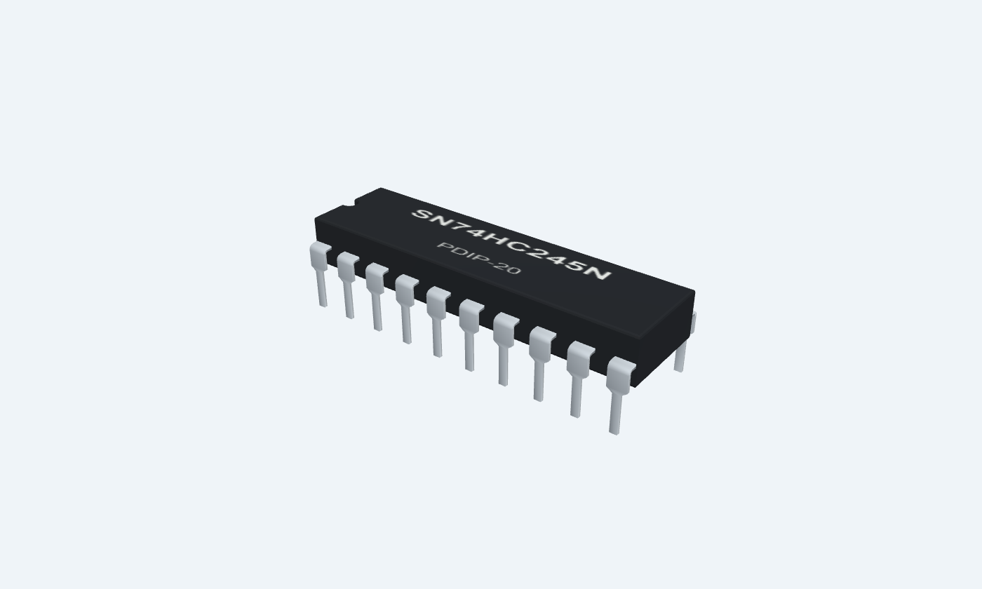
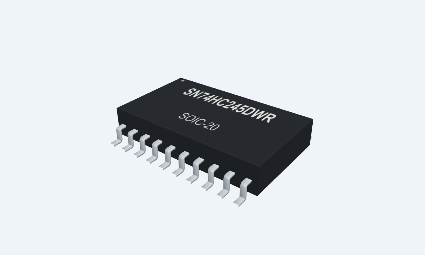
Eight logic channels. One direction. A controlled handoff.
74HC245 moves eight logic signals between two buses. A direction input selects which side receives data, and one active-LOW enable controls all eight channels together. There is no clock, latch or stored byte. With DIR HIGH, each B output follows its matching A input. With DIR LOW, data travels from B to A. A HIGH enable releases both output banks, so external circuitry can take ownership without two active drivers fighting. Both sides operate from the same supply. This page covers TI SN74HC245N PDIP and SN74HC245DWR wide SOIC packages, with the SN74 temperature range of −40 to +85°C. The 5 V example fixes direction from eight switches to eight LED branches and shows the byte A5 hexadecimal. Every input and disabled output has a defined external bias.
Click a lead or use the arrow keys. Top view
HIGH selects A-to-B; LOW selects B-to-A while /OE is LOW.
Tie to +5 V in this one-way demonstration.
Disable the bus before changing direction. Release the old source before enabling the new one.
Channel 1 A-side port. Input with DIR HIGH; output with DIR LOW.
Connect a switch to +5 V and a separate 10 kΩ pull-down to GND. A1 corresponds to B1.
Never drive this node externally while the transceiver is driving it.
Channel 2 A-side port. Input with DIR HIGH; output with DIR LOW.
Connect a switch to +5 V and a separate 10 kΩ pull-down to GND. A2 corresponds to B2.
Never drive this node externally while the transceiver is driving it.
Channel 3 A-side port. Input with DIR HIGH; output with DIR LOW.
Connect a switch to +5 V and a separate 10 kΩ pull-down to GND. A3 corresponds to B3.
Never drive this node externally while the transceiver is driving it.
Channel 4 A-side port. Input with DIR HIGH; output with DIR LOW.
Connect a switch to +5 V and a separate 10 kΩ pull-down to GND. A4 corresponds to B4.
Never drive this node externally while the transceiver is driving it.
Channel 5 A-side port. Input with DIR HIGH; output with DIR LOW.
Connect a switch to +5 V and a separate 10 kΩ pull-down to GND. A5 corresponds to B5.
Never drive this node externally while the transceiver is driving it.
Channel 6 A-side port. Input with DIR HIGH; output with DIR LOW.
Connect a switch to +5 V and a separate 10 kΩ pull-down to GND. A6 corresponds to B6.
Never drive this node externally while the transceiver is driving it.
Channel 7 A-side port. Input with DIR HIGH; output with DIR LOW.
Connect a switch to +5 V and a separate 10 kΩ pull-down to GND. A7 corresponds to B7.
Never drive this node externally while the transceiver is driving it.
Channel 8 A-side port. Input with DIR HIGH; output with DIR LOW.
Connect a switch to +5 V and a separate 10 kΩ pull-down to GND. A8 corresponds to B8.
Never drive this node externally while the transceiver is driving it.
Common return for both buses and controls.
Connect to supply return and the bypass capacitor.
Channel 8 B-side port. Output with DIR HIGH; input with DIR LOW.
Connect through 1 kΩ to an LED anode; cathode to GND. A 100 kΩ pull-down defines the disabled node.
The two ports share one supply domain. This is not a dual-supply level translator.
Channel 7 B-side port. Output with DIR HIGH; input with DIR LOW.
Connect through 1 kΩ to an LED anode; cathode to GND. A 100 kΩ pull-down defines the disabled node.
The two ports share one supply domain. This is not a dual-supply level translator.
Channel 6 B-side port. Output with DIR HIGH; input with DIR LOW.
Connect through 1 kΩ to an LED anode; cathode to GND. A 100 kΩ pull-down defines the disabled node.
The two ports share one supply domain. This is not a dual-supply level translator.
Channel 5 B-side port. Output with DIR HIGH; input with DIR LOW.
Connect through 1 kΩ to an LED anode; cathode to GND. A 100 kΩ pull-down defines the disabled node.
The two ports share one supply domain. This is not a dual-supply level translator.
Channel 4 B-side port. Output with DIR HIGH; input with DIR LOW.
Connect through 1 kΩ to an LED anode; cathode to GND. A 100 kΩ pull-down defines the disabled node.
The two ports share one supply domain. This is not a dual-supply level translator.
Channel 3 B-side port. Output with DIR HIGH; input with DIR LOW.
Connect through 1 kΩ to an LED anode; cathode to GND. A 100 kΩ pull-down defines the disabled node.
The two ports share one supply domain. This is not a dual-supply level translator.
Channel 2 B-side port. Output with DIR HIGH; input with DIR LOW.
Connect through 1 kΩ to an LED anode; cathode to GND. A 100 kΩ pull-down defines the disabled node.
The two ports share one supply domain. This is not a dual-supply level translator.
Channel 1 B-side port. Output with DIR HIGH; input with DIR LOW.
Connect through 1 kΩ to an LED anode; cathode to GND. A 100 kΩ pull-down defines the disabled node.
The two ports share one supply domain. This is not a dual-supply level translator.
LOW enables the direction-selected paths; HIGH releases both sets of drivers.
Use 10 kΩ to +5 V and a switch to GND. Close it to enable.
HIGH means high impedance, not a driven LOW.
Powers the logic and output drivers.
Use +5 V with 100 nF directly between pins 20 and 10.
Recommended operating supply: 2–6 V.
Octal bidirectional bus transceiver
Eight noninverting paths share DIR and /OE. The selected output bank drives only while /OE is LOW; the other bank receives. /OE HIGH releases both banks.
SN74HC245N
Key parameters and their test conditions
Follows the selected physical package
Select a pin to open its function, electrical notes and wiring guidance.
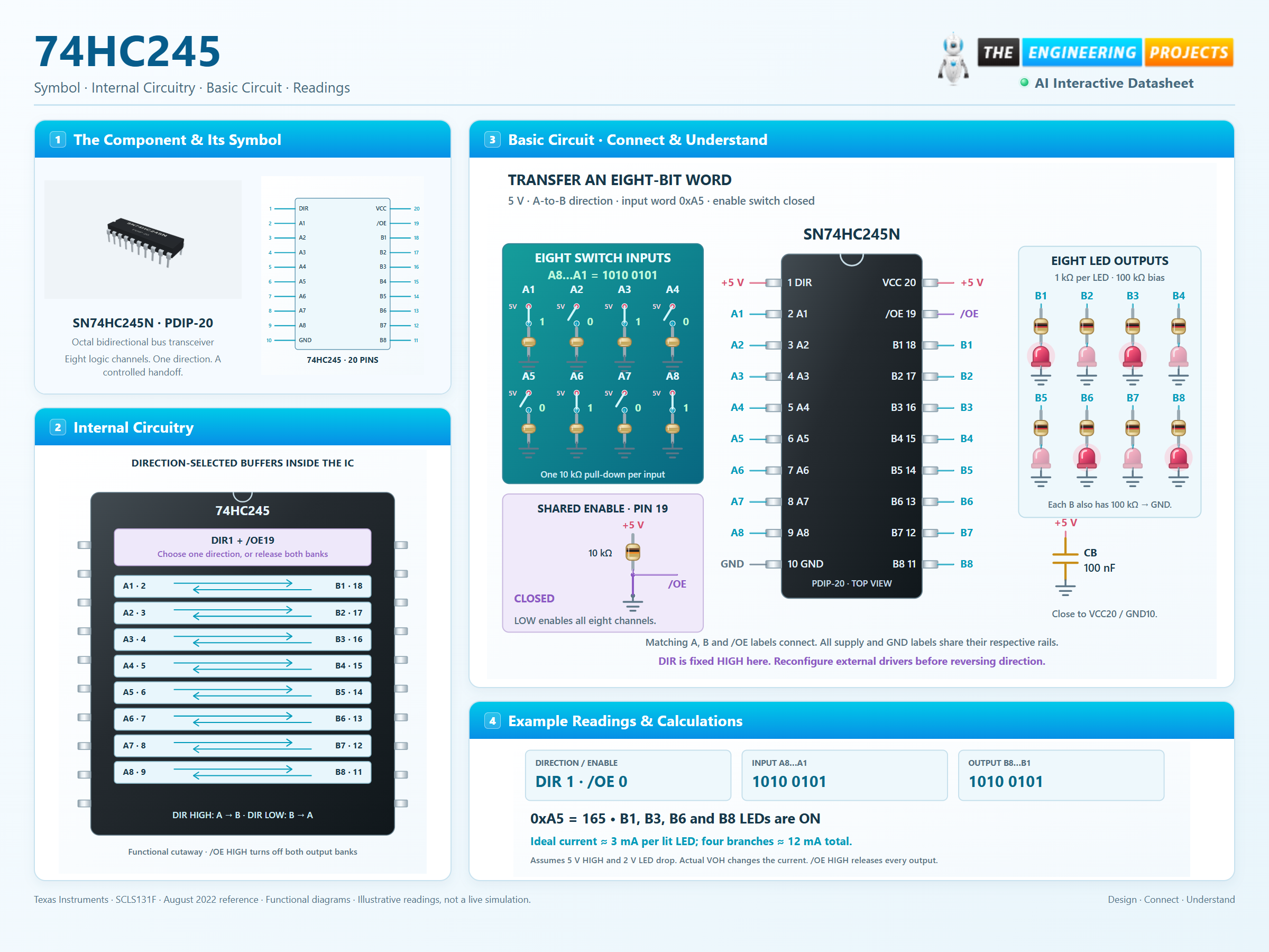
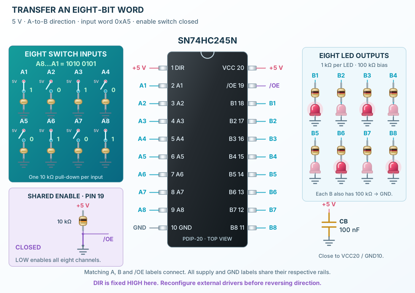
Eight switches establish A1 through A8. A1 is the least significant bit in this example. A8…A1 = 1010 0101 gives hexadecimal A5.
DIR pin 1 is held HIGH. Closing the /OE switch pulls pin 19 LOW and enables A-to-B transfer.
B1, B3, B6 and B8 light their LEDs. Opening /OE releases all eight drivers; external pull-downs define the disabled nodes.
Disable, release the old source, select direction and enable the new transfer. High impedance is not a logic LOW, and a shared supply does not make HC a universal voltage translator.
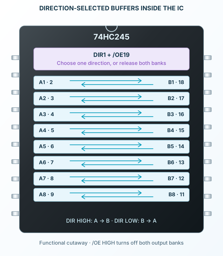
Select a pin to explore its function and connection.
| Pin | Signal | Type | Function |
|---|---|---|---|
| DIR | Direction input | HIGH selects A-to-B; LOW selects B-to-A while /OE is LOW. | |
| A1 | Bidirectional logic port | Channel 1 A-side port. Input with DIR HIGH; output with DIR LOW. | |
| A2 | Bidirectional logic port | Channel 2 A-side port. Input with DIR HIGH; output with DIR LOW. | |
| A3 | Bidirectional logic port | Channel 3 A-side port. Input with DIR HIGH; output with DIR LOW. | |
| A4 | Bidirectional logic port | Channel 4 A-side port. Input with DIR HIGH; output with DIR LOW. | |
| A5 | Bidirectional logic port | Channel 5 A-side port. Input with DIR HIGH; output with DIR LOW. | |
| A6 | Bidirectional logic port | Channel 6 A-side port. Input with DIR HIGH; output with DIR LOW. | |
| A7 | Bidirectional logic port | Channel 7 A-side port. Input with DIR HIGH; output with DIR LOW. | |
| A8 | Bidirectional logic port | Channel 8 A-side port. Input with DIR HIGH; output with DIR LOW. | |
| GND | Ground return | Common return for both buses and controls. | |
| B8 | Bidirectional logic port | Channel 8 B-side port. Output with DIR HIGH; input with DIR LOW. | |
| B7 | Bidirectional logic port | Channel 7 B-side port. Output with DIR HIGH; input with DIR LOW. | |
| B6 | Bidirectional logic port | Channel 6 B-side port. Output with DIR HIGH; input with DIR LOW. | |
| B5 | Bidirectional logic port | Channel 5 B-side port. Output with DIR HIGH; input with DIR LOW. | |
| B4 | Bidirectional logic port | Channel 4 B-side port. Output with DIR HIGH; input with DIR LOW. | |
| B3 | Bidirectional logic port | Channel 3 B-side port. Output with DIR HIGH; input with DIR LOW. | |
| B2 | Bidirectional logic port | Channel 2 B-side port. Output with DIR HIGH; input with DIR LOW. | |
| B1 | Bidirectional logic port | Channel 1 B-side port. Output with DIR HIGH; input with DIR LOW. | |
| /OE | Active-LOW output enable | LOW enables the direction-selected paths; HIGH releases both sets of drivers. | |
| VCC | Positive supply | Powers the logic and output drivers. |
No pins match. Try a signal name or choose All pins.
Shared by all eight channels
| Parameter | Value | Conditions / notes |
|---|---|---|
| /OE LOW; DIR HIGH | A inputs → B outputs | Noninverting, asynchronous transfer |
| /OE LOW; DIR LOW | B inputs → A outputs | Reverse direction |
| /OE HIGH; DIR either level | Both output banks high impedance | External bias determines node voltages |
| Output state | LOW, HIGH or Z drive condition | Z is not a third voltage |
| Data storage | None | Output follows after propagation delay; no clock |
| Direction changes | Disable first; release old source | Prevent bus contention during handoff |
No specifications match. Try a parameter name or a unit.
The illustrated switch/LED circuit is wired for A-to-B only. Reconfigure external sources before reversing direction.
SN74HC245N · PDIP-20
| Parameter | Value | Conditions / notes |
|---|---|---|
| Channel 1 | A1 pin 2 ↔ B1 pin 18 | Same logic polarity in either direction |
| Channel 2 | A2 pin 3 ↔ B2 pin 17 | Same logic polarity in either direction |
| Channel 3 | A3 pin 4 ↔ B3 pin 16 | Same logic polarity in either direction |
| Channel 4 | A4 pin 5 ↔ B4 pin 15 | Same logic polarity in either direction |
| Channel 5 | A5 pin 6 ↔ B5 pin 14 | Same logic polarity in either direction |
| Channel 6 | A6 pin 7 ↔ B6 pin 13 | Same logic polarity in either direction |
| Channel 7 | A7 pin 8 ↔ B7 pin 12 | Same logic polarity in either direction |
| Channel 8 | A8 pin 9 ↔ B8 pin 11 | Same logic polarity in either direction |
| Control pins | DIR 1; /OE 19 | One direction and one enable for the entire byte |
| Power pins | VCC20; GND10 | 100 nF bypass placed close to the package |
No specifications match. Try a parameter name or a unit.
The physical arrangement differs from latch/register ICs: this device does not capture or retain data.
SN74 operating conditions
| Parameter | Value | Conditions / notes |
|---|---|---|
| Recommended supply | 2–6 V | 5 V demonstration |
| Operating temperature | −40 to +85°C | SN74 grade; do not substitute SN54 limits |
| HIGH input at 4.5 V | At least 3.15 V | HC CMOS threshold |
| LOW input at 4.5 V | At most 1.35 V | Intermediate region is unspecified |
| Thresholds at 2 V | HIGH ≥1.5 V; LOW ≤0.5 V | Manufacturer test point |
| Thresholds at 6 V | HIGH ≥4.2 V; LOW ≤1.8 V | A 3.3 V source does not guarantee HIGH here |
| Input rise/fall time maximum | 1000 / 500 / 400 ns | At 2 / 4.5 / 6 V |
| Normal port voltage | Between GND and VCC | Respect power sequencing and clamp-current limits |
No specifications match. Try a parameter name or a unit.
A single VCC powers both buses. Use a suitable level translator where independent voltage domains are required.
Defined test conditions
| Parameter | Value | Conditions / notes |
|---|---|---|
| HIGH output at 4.5 V, −6 mA | 4.3 V typical; 3.98 V minimum at 25°C | 3.84 V minimum across SN74 temperature range |
| LOW output at 4.5 V, 6 mA | 0.17 V typical; 0.26 V maximum at 25°C | 0.33 V maximum across SN74 temperature range |
| Light-load output at 4.5 V | HIGH ≥4.4 V; LOW ≤0.1 V | 20 µA load |
| Disabled-port leakage at 6 V | ±0.01 µA typical; ±0.5 µA maximum at 25°C | ±5 µA maximum across SN74 range |
| DIR / OE input leakage at 6 V | ±0.1 µA maximum at 25°C | ±1 µA maximum across temperature |
| Static supply current at 6 V | 8 µA max at 25°C; 80 µA max over range | Inputs at supply rails, no output load |
| Control input capacitance | 3 pF typical; 10 pF maximum | DIR / OE, 2–6 V |
No specifications match. Try a parameter name or a unit.
Output drive and supply current are separate quantities. Add the loads of all active channels when checking package current.
4.5 V · CL = 50 pF
| Parameter | Value | Conditions / notes |
|---|---|---|
| Data propagation A↔B | 15 ns typical; 21 ns maximum at 25°C | 26 ns maximum across −40…85°C |
| Enable /OE to output | 23 ns typical; 46 ns maximum at 25°C | 58 ns maximum across temperature |
| Disable /OE to Z | 25 ns typical; 40 ns maximum at 25°C | 50 ns maximum across temperature |
| Output transition | 8 ns typical; 12 ns maximum at 25°C | 15 ns maximum across temperature |
| Data delay with 150 pF load | 18 ns typical; 27 ns max at 25°C | 34 ns maximum across SN74 temperature range |
| Break-before-make timing | Account for worst-case delay and control skew | A released node may settle slowly through external bias |
No specifications match. Try a parameter name or a unit.
Typical values are descriptive, not guaranteed design limits. The headline 12 ns value is the 6 V, 50 pF typical data delay.
5 V · DIR HIGH · /OE LOW
| Parameter | Value | Conditions / notes |
|---|---|---|
| Input word | A8…A1 = 1010 0101 | 0xA5 = decimal 165 |
| Input switches | Each A pin → switch → +5 V | Separate 10 kΩ from each A pin to GND |
| Output LEDs | Each B pin → 1 kΩ → LED anode → cathode to GND | One resistor per LED |
| Disabled-output bias | 100 kΩ from every B pin to GND | Defines nodes when the IC releases its drivers |
| Enable control | 10 kΩ pull-up on pin 19; switch to GND | Open = disabled, closed = enabled |
| Illustrated LEDs on | B1, B3, B6 and B8 | Four HIGH outputs |
| Ideal current | About 3 mA per lit red LED, about 12 mA total | Assumes 5 V output and 2 V LED drop; actual VOH changes it |
| Local bypass | 100 nF from VCC20 to GND10 | Short connection loop |
No specifications match. Try a parameter name or a unit.
The drawn switch positions are illustrative steady states. No clock is driven by the switches.
Stress ratings are not operating targets
| Parameter | Value | Conditions / notes |
|---|---|---|
| Absolute VCC maximum | 7 V | Normal operating maximum is 6 V |
| Absolute per-output current | ±35 mA | Use the specified loaded output levels for real designs |
| Absolute VCC / GND current | ±70 mA | Total package current, not per channel |
| Absolute clamp current | ±20 mA | Avoid normal use of protection diodes as voltage conversion |
| Bus contention | Never enable opposing driven levels | Disable before changing source ownership |
| Unused channel bias | Hold inputs at a valid rail | Use resistive bias if a port may become an output |
| Routing | Short returns and close bypass | Reduce capacitive load and ringing |
No specifications match. Try a parameter name or a unit.
Do not power LEDs, relays or other loads without checking their load currents and required external drivers.
Transfer a byte between compatible same-supply logic domains with controlled ownership.
Manufacturer application guideSelect which side supplies data and release both banks when idle.
Manufacturer application guideObserve an eight-bit pattern with separate current-limiting resistors and modest loads.
Manufacturer application guideFind 74HC245 in the Components Library to place its schematic symbol and connect its pins.
Reference page · circuit simulation model not yet availableOpen ProTech