Real View
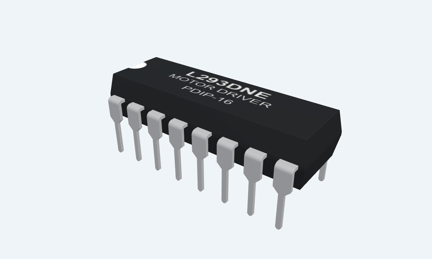
Choose direction, brake or coast with a pair of logic signals.
L293D combines four half-H drivers in a 16-pin package. Pair two outputs around a DC motor to reverse the voltage across it, or use the four channels for other inductive loads. A separate logic supply drives the control circuitry, while the motor supply feeds the output stages. Enable pins control the outputs in pairs; disabling a pair puts both outputs into high impedance. This page covers the TI L293DNE PDIP-16 device, including its internal clamp diodes and 600 mA per-channel rating. Motor stall current, driver voltage drop and package heating still determine whether a load is suitable.
Select a pin to explore its connection
Click a lead or use the arrow keys. Top view
Enables outputs 1Y and 2Y together. LOW makes both high impedance.
Connect to a defined logic control or PWM signal.
Add a pull-down so the motor stays disabled during controller reset.
Controls the first half-bridge when enabled.
First direction-control signal.
First motor terminal for bridge A.
Connect to one motor lead; the other goes to 2Y.
Output has a voltage drop under load.
Supply return and package thermal connection.
Connect with pins 5, 12 and 13 to a ground plane.
Supply return and package thermal connection.
Connect all four ground pins.
Second motor terminal for bridge A.
Connect to the other motor lead.
Controls the second half-bridge when enabled.
Second direction-control signal.
Supplies the four power output stages.
Use +12 V in this example; decouple locally and add bulk capacitance.
The reviewed TI operating table requires VCC2 ≥ VCC1 and ≤36 V.
Enables outputs 3Y and 4Y together.
Tie LOW when the second bridge is unused.
Controls the third half-bridge.
Tie LOW if unused.
First output of bridge B.
Leave open if bridge B is unused.
Supply return and thermal connection.
Connect to the same ground plane as pins 4, 5 and 13.
Supply return and thermal connection.
Connect all four ground pins.
Second output of bridge B.
Leave open if bridge B is unused.
Controls the fourth half-bridge.
Tie LOW if unused.
Supplies internal logic translation.
Use +5 V and a 100 nF bypass to GND.
Keep the logic and motor supply returns connected.
Four half-bridges provide two reversible output pairs. The L293D includes clamp diodes, but current, supply energy and heat still need a suitable design.
L293DNE · PDIP-16
| Property | Details |
|---|---|
| Manufacturer | Texas Instruments |
| Part number | L293DNE |
| Package | PDIP-16 |
| Connections | 16 pins |
| Mounting | Through-hole |
| Lead pitch | 2.54 mm |
| Package code | dip |
| Thermal reference | Board and package dependent; see manufacturer data |
TI L293DNE
Scroll sideways to see all columns.
| Parameter | Value | Conditions / notes |
|---|---|---|
| Logic supply VCC1 | 4.5–7 V | Use 5 V in this example |
| Motor supply VCC2 | VCC1 to 36 V | Separate motor power rail |
| Ambient temperature | 0 to 70°C | Operating range |
| Input HIGH | ≥2.3 V | At VCC1 = 5 V |
| Input LOW | ≤1.5 V | Use normal 0 V logic LOW |
| Ground connections | 4, 5, 12, 13 | All required; also conduct heat |
No specifications match. Try a parameter name or a unit.
Do not confuse L293D current ratings with the higher-current L293.
Motor between 1Y3 and 2Y6
Scroll sideways to see all columns.
| Parameter | Value | Conditions / notes |
|---|---|---|
| EN LOW; A1/A2 any | Coast · outputs Z / Z | No commanded drive; clamp paths remain |
| EN HIGH; A1 HIGH, A2 LOW | Direction A | 1Y HIGH; 2Y LOW |
| EN HIGH; A1 LOW, A2 HIGH | Direction B | 1Y LOW; 2Y HIGH |
| EN HIGH; A1 LOW, A2 LOW | Brake to GND | Both outputs LOW |
| EN HIGH; A1 HIGH, A2 HIGH | Brake to motor rail | Both outputs HIGH |
No specifications match. Try a parameter name or a unit.
Physical clockwise direction depends on motor wiring. Braking does not stop motion instantaneously.
L293D
Scroll sideways to see all columns.
| Parameter | Value | Conditions / notes |
|---|---|---|
| Continuous output current | ±600 mA per channel | Respect package thermal constraints |
| HIGH output at −0.6 A | VCC2 − 1.4 V typical | VCC2 − 1.8 V minimum |
| LOW output at +0.6 A | 1.2 V typical | 1.8 V maximum |
| Typical bridge loss at 0.6 A | 1.56 W | 0.6 A × (1.4 + 1.2 V), excluding logic losses |
| Typical motor voltage at 12 V | 9.4 V at 0.6 A | 12 − 1.4 − 1.2; not a regulated output |
| Clamp diodes | Built in | Inductive transient current returns to the rails |
No specifications match. Try a parameter name or a unit.
Voltage drops depend on current and temperature. The 9.4 V example is not valid for every load.
5 V logic · 12 V motor rail
Scroll sideways to see all columns.
| Parameter | Value | Conditions / notes |
|---|---|---|
| Enable1 | Controller output with 10 kΩ pull-down | Motor disabled while controller output floats |
| Direction inputs2 and7 | Defined controller outputs | Change direction with a suitable stop/dead-time strategy |
| Motor leads | Outputs3 and6 | Choose a motor with acceptable stall current |
| Logic bypass | 100 nF | VCC1 pin16 to GND |
| Motor bypass | 100 nF + suitable bulk capacitor | VCC2 pin8 to GND; example bulk 100 µF |
| Unused bridge | Pins9,10,15 LOW | Outputs11 and14 open |
| Return | Controller, both supplies and all GND pins | Common reference |
No specifications match. Try a parameter name or a unit.
Bulk capacitance is an example; account for wiring, motor energy and the supply’s ability to absorb current.
L293DNE
Scroll sideways to see all columns.
| Parameter | Value | Conditions / notes |
|---|---|---|
| Reviewed package | PDIP-16 | TI L293DNE; 2.54 mm lead pitch |
| Peak output current | ±1.2 A | Nonrepetitive; duration ≤100 µs; stress rating |
| Maximum junction temperature | 150°C | Absolute maximum; design for lower operating temperature |
| Storage temperature | −65 to +150°C | Unpowered |
| Board thermal resistance | 36.4°C/W reference | TI JEDEC test-board condition; real layout differs |
No specifications match. Try a parameter name or a unit.
This page does not substitute a different manufacturer’s SMD package or pin map.
Select a pin for its function, connection guidance and electrical notes.
Follow the labeled connections and functional stages
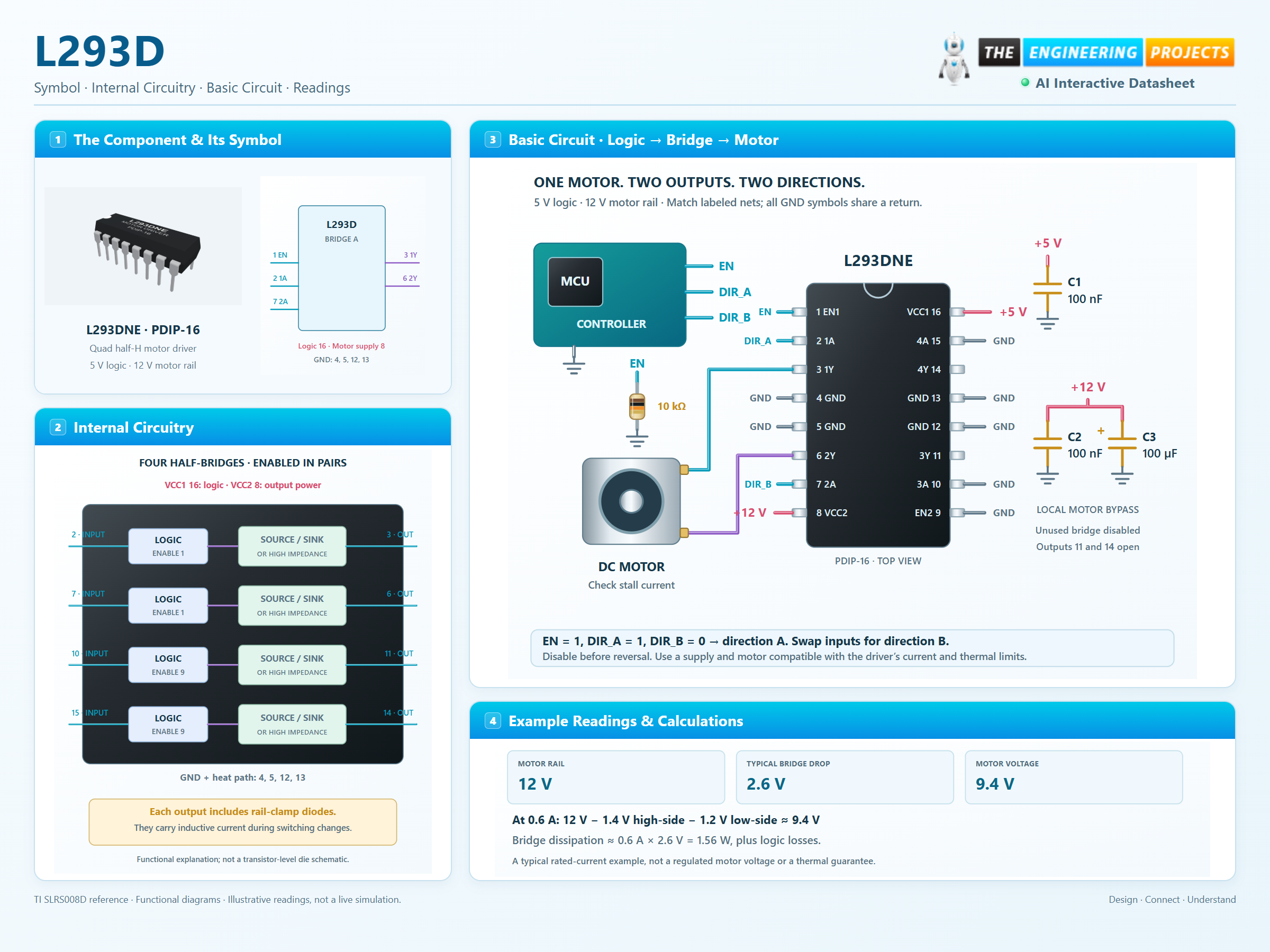
3 stages · Explore one step at a time
Set 1,2EN HIGH to make 1Y and 2Y follow their corresponding inputs. Disable the pair to release both motor leads into high impedance.
Opposite input states apply opposite polarities across the motor. Swapping the inputs reverses the commanded direction.
Equal enabled outputs short the motor terminals to the same rail for dynamic braking. Disabled outputs let the motor coast; stored inductive current still uses the clamp paths.
Switch the inputs to explore one complete motor bridge.
Enable JavaScript to explore bridge control.
Logic-state explorer only. The colored motor indicates commanded direction, not simulated speed. Current, inertia, switching time, voltage drop, clamp transients and heating are not calculated.
A controller, one real IC and an unmistakable motor connection.
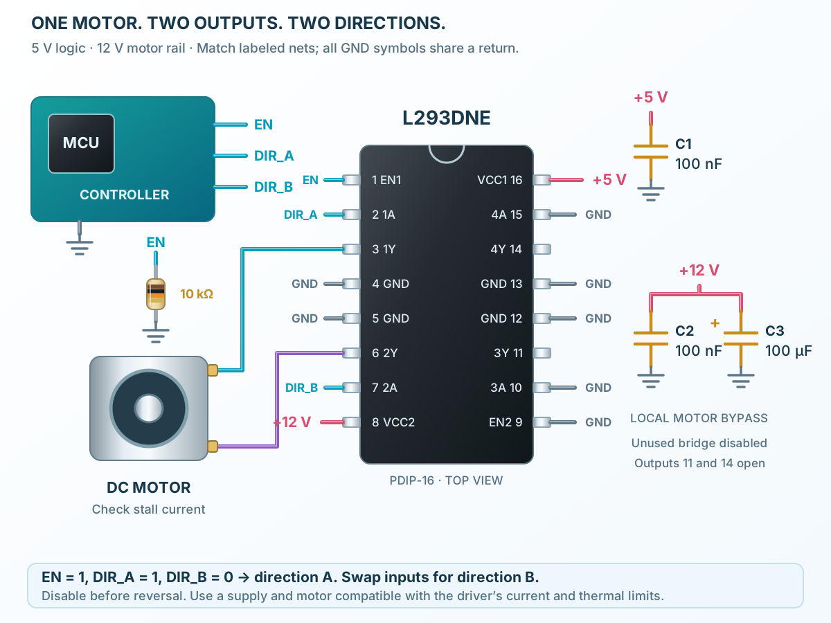
Follow the component values and pin connections
Connect controller GND to the driver and both supply returns.
The motor rail feeds pin 8. Logic power goes to pin 16.
The motor is between 1Y and 2Y, not between one output and ground.
Four half-bridges, paired enables and internal clamp paths.
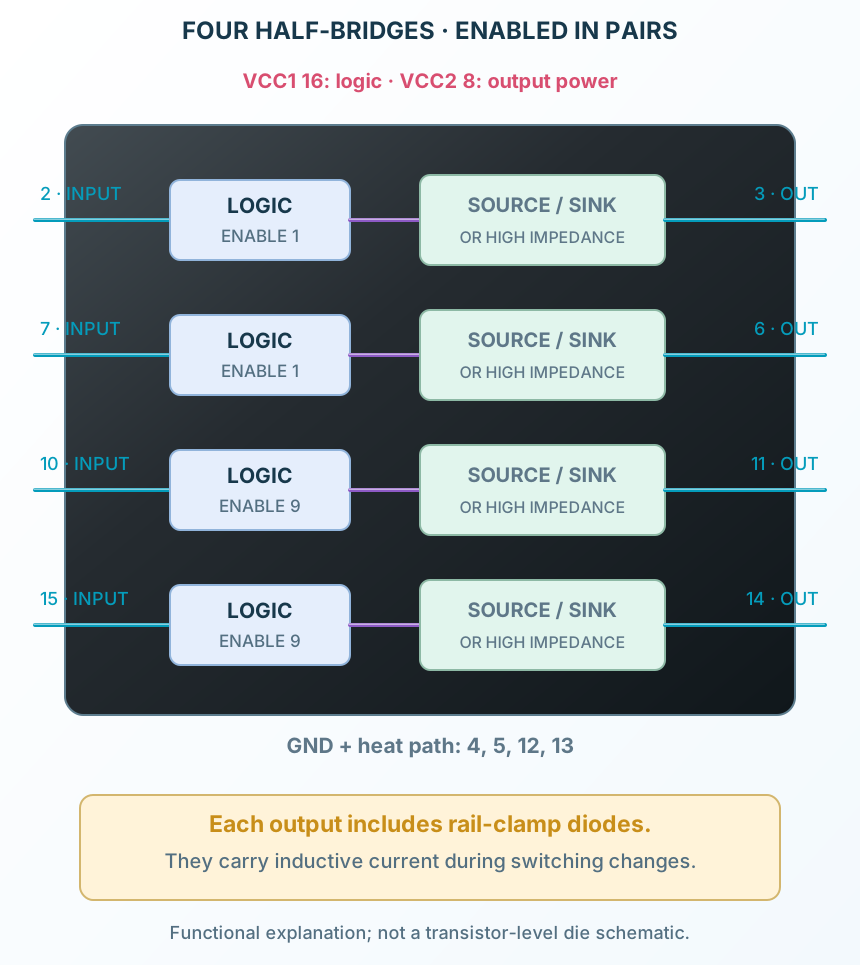
Select a stage to see its role and connections
The input and enable logic runs from VCC1.
Each output can source from VCC2, sink to GND, or become high impedance.
Internal clamp diodes provide paths for inductive current when switching changes. The supply network must absorb or store that energy.
Signal names, electrical functions and connection guidance
Scroll within the table to see all columns and rows.
| Pin | Signal | Type | Function & connection |
|---|---|---|---|
| 1,2EN | Active-HIGH enable | Enables outputs 1Y and 2Y together. LOW makes both high impedance.Connection guidanceConnect to a defined logic control or PWM signal. Add a pull-down so the motor stays disabled during controller reset. | |
| 1A | Driver 1 input | Controls the first half-bridge when enabled.Connection guidanceFirst direction-control signal. | |
| 1Y | Driver 1 output | First motor terminal for bridge A.Connection guidanceConnect to one motor lead; the other goes to 2Y. Output has a voltage drop under load. | |
| GND | Ground and heat path | Supply return and package thermal connection.Connection guidanceConnect with pins 5, 12 and 13 to a ground plane. | |
| GND | Ground and heat path | Supply return and package thermal connection.Connection guidanceConnect all four ground pins. | |
| 2Y | Driver 2 output | Second motor terminal for bridge A.Connection guidanceConnect to the other motor lead. | |
| 2A | Driver 2 input | Controls the second half-bridge when enabled.Connection guidanceSecond direction-control signal. | |
| VCC2 | Motor supply | Supplies the four power output stages.Connection guidanceUse +12 V in this example; decouple locally and add bulk capacitance. The reviewed TI operating table requires VCC2 ≥ VCC1 and ≤36 V. | |
| 3,4EN | Active-HIGH enable | Enables outputs 3Y and 4Y together.Connection guidanceTie LOW when the second bridge is unused. | |
| 3A | Driver 3 input | Controls the third half-bridge.Connection guidanceTie LOW if unused. | |
| 3Y | Driver 3 output | First output of bridge B.Connection guidanceLeave open if bridge B is unused. | |
| GND | Ground and heat path | Supply return and thermal connection.Connection guidanceConnect to the same ground plane as pins 4, 5 and 13. | |
| GND | Ground and heat path | Supply return and thermal connection.Connection guidanceConnect all four ground pins. | |
| 4Y | Driver 4 output | Second output of bridge B.Connection guidanceLeave open if bridge B is unused. | |
| 4A | Driver 4 input | Controls the fourth half-bridge.Connection guidanceTie LOW if unused. | |
| VCC1 | Logic supply | Supplies internal logic translation.Connection guidanceUse +5 V and a 100 nF bypass to GND. Keep the logic and motor supply returns connected. |
No pins match these filters. Try another signal name or reset the filters.
TI L293DNE
Scroll within the table to see all columns and rows.
| Parameter | Value | Conditions / notes |
|---|---|---|
| Logic supply VCC1 | 4.5–7 V | Use 5 V in this example |
| Motor supply VCC2 | VCC1 to 36 V | Separate motor power rail |
| Ambient temperature | 0 to 70°C | Operating range |
| Input HIGH | ≥2.3 V | At VCC1 = 5 V |
| Input LOW | ≤1.5 V | Use normal 0 V logic LOW |
| Ground connections | 4, 5, 12, 13 | All required; also conduct heat |
No specifications match. Try a parameter name or a unit.
Do not confuse L293D current ratings with the higher-current L293.
Motor between 1Y3 and 2Y6
Scroll within the table to see all columns and rows.
| Parameter | Value | Conditions / notes |
|---|---|---|
| EN LOW; A1/A2 any | Coast · outputs Z / Z | No commanded drive; clamp paths remain |
| EN HIGH; A1 HIGH, A2 LOW | Direction A | 1Y HIGH; 2Y LOW |
| EN HIGH; A1 LOW, A2 HIGH | Direction B | 1Y LOW; 2Y HIGH |
| EN HIGH; A1 LOW, A2 LOW | Brake to GND | Both outputs LOW |
| EN HIGH; A1 HIGH, A2 HIGH | Brake to motor rail | Both outputs HIGH |
No specifications match. Try a parameter name or a unit.
Physical clockwise direction depends on motor wiring. Braking does not stop motion instantaneously.
L293D
Scroll within the table to see all columns and rows.
| Parameter | Value | Conditions / notes |
|---|---|---|
| Continuous output current | ±600 mA per channel | Respect package thermal constraints |
| HIGH output at −0.6 A | VCC2 − 1.4 V typical | VCC2 − 1.8 V minimum |
| LOW output at +0.6 A | 1.2 V typical | 1.8 V maximum |
| Typical bridge loss at 0.6 A | 1.56 W | 0.6 A × (1.4 + 1.2 V), excluding logic losses |
| Typical motor voltage at 12 V | 9.4 V at 0.6 A | 12 − 1.4 − 1.2; not a regulated output |
| Clamp diodes | Built in | Inductive transient current returns to the rails |
No specifications match. Try a parameter name or a unit.
Voltage drops depend on current and temperature. The 9.4 V example is not valid for every load.
5 V logic · 12 V motor rail
Scroll within the table to see all columns and rows.
| Parameter | Value | Conditions / notes |
|---|---|---|
| Enable1 | Controller output with 10 kΩ pull-down | Motor disabled while controller output floats |
| Direction inputs2 and7 | Defined controller outputs | Change direction with a suitable stop/dead-time strategy |
| Motor leads | Outputs3 and6 | Choose a motor with acceptable stall current |
| Logic bypass | 100 nF | VCC1 pin16 to GND |
| Motor bypass | 100 nF + suitable bulk capacitor | VCC2 pin8 to GND; example bulk 100 µF |
| Unused bridge | Pins9,10,15 LOW | Outputs11 and14 open |
| Return | Controller, both supplies and all GND pins | Common reference |
No specifications match. Try a parameter name or a unit.
Bulk capacitance is an example; account for wiring, motor energy and the supply’s ability to absorb current.
L293DNE
Scroll within the table to see all columns and rows.
| Parameter | Value | Conditions / notes |
|---|---|---|
| Reviewed package | PDIP-16 | TI L293DNE; 2.54 mm lead pitch |
| Peak output current | ±1.2 A | Nonrepetitive; duration ≤100 µs; stress rating |
| Maximum junction temperature | 150°C | Absolute maximum; design for lower operating temperature |
| Storage temperature | −65 to +150°C | Unpowered |
| Board thermal resistance | 36.4°C/W reference | TI JEDEC test-board condition; real layout differs |
No specifications match. Try a parameter name or a unit.
This page does not substitute a different manufacturer’s SMD package or pin map.
No matching rowsTry a pin name, parameter, unit or test condition, or reset the filters.
Two half-bridges form a reversible motor output with separate enable control.
Manufacturer application guideUse both bridge pairs to drive two windings with an appropriate current and stepping strategy.
Manufacturer application guideDrive inductive loads while accounting for clamp paths, current and package dissipation.
Manufacturer application guideFind L293D in the Components Library to place its schematic symbol and connect its pins.
Reference page · circuit simulation model not yet availableOpen ProTech