LM1458Dual general-purpose operational amplifier
Two analog amplifiers, with independent feedback and shared rails.
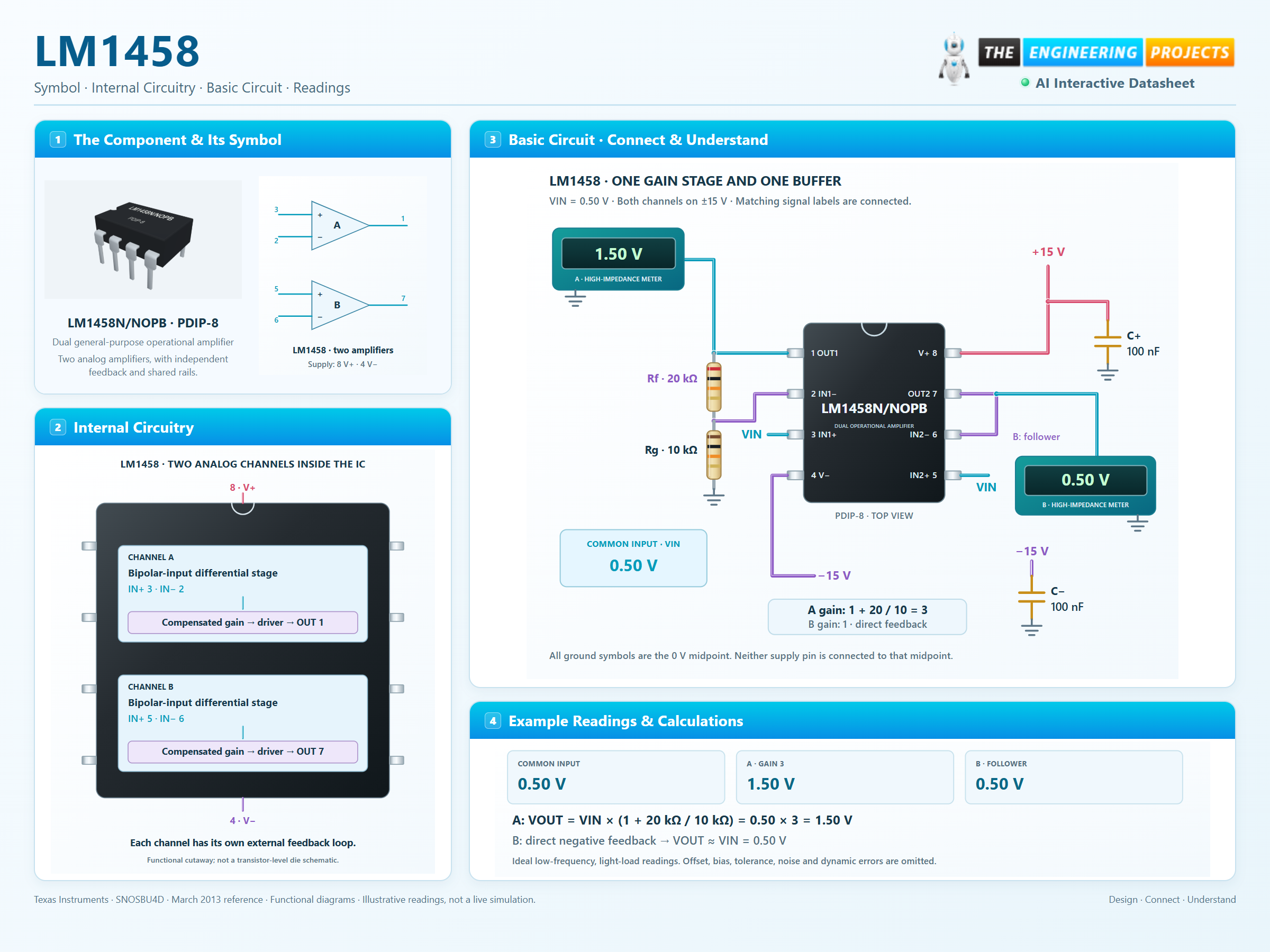
LM1458 contains two internally compensated, general-purpose operational amplifiers in one eight-pin package. Each amplifier has its own input pair and output, while both share the positive and negative supply rails. External feedback determines the useful closed-loop gain. This page uses the commercial LM1458N/NOPB PDIP-8 and LM1458M/NOPB SOIC-8 parts, specified over 0 to 70°C. The pinout and downloadable PCB footprint follow the selected package; LM1558 military-temperature limits are not used. The example applies 0.50 V to both channels on ±15 V rails. A 20 kΩ / 10 kΩ feedback network gives channel A an ideal output of 1.50 V, while channel B follows at 0.50 V. Real errors depend on offset, input bias current, resistor tolerance, load and signal frequency.
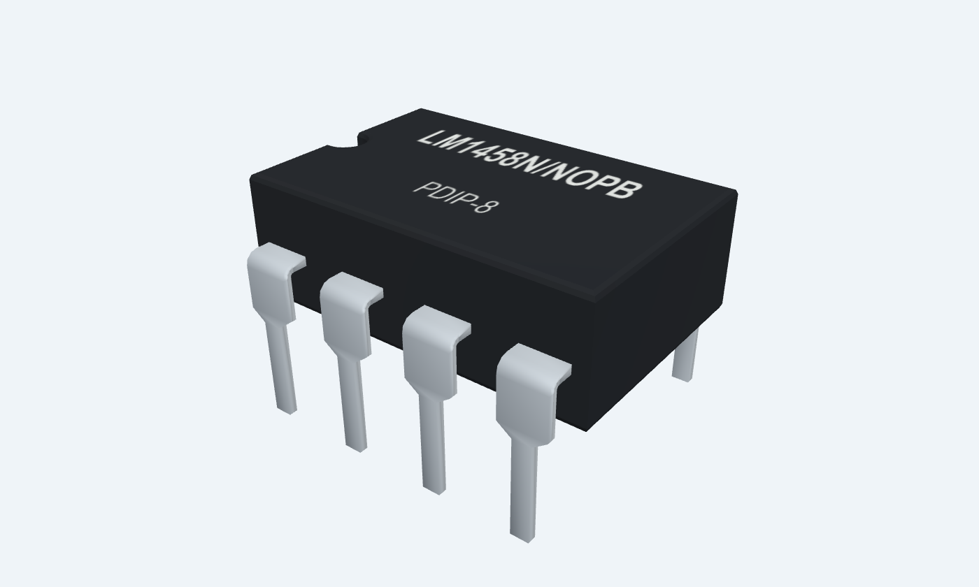
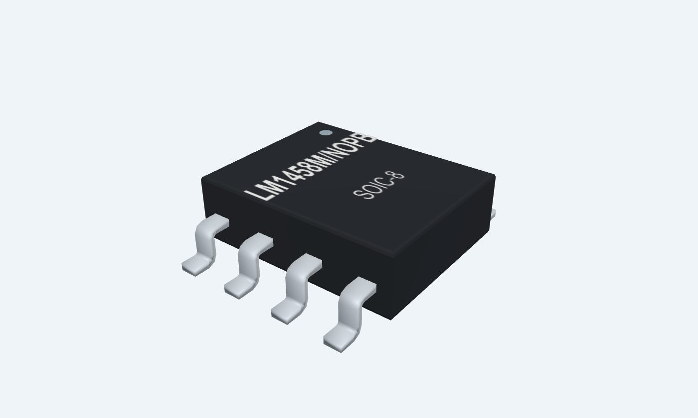

8Physical pins
LM1458N/NOPBPDIP-8
Manufacturer-referencedTexas Instruments
Pin diagram
Select a pin to explore its connection
Highlight
LM1458PDIP-8Top view
LM1458SOIC-8Top view
Click a lead or use the arrow keys. Top view
PIN 1 · Analog outputs
Analog outputOUT1
Function
Channel A output.
How to connect
Return to IN1− through 20 kΩ; connect a high-impedance meter.
PIN 2 · Analog inputs
Inverting inputIN1−
Function
Channel A negative-feedback node.
How to connect
Join 20 kΩ from OUT1 and 10 kΩ to signal ground.
PIN 3 · Analog inputs
Non-inverting inputIN1+
Function
Channel A signal input.
How to connect
Apply VIN = 0.50 V relative to the 0 V midpoint.
PIN 4 · Supply
Negative supplyV−
Function
Negative rail shared by both amplifiers.
How to connect
Connect −15 V; bypass locally to 0 V with 100 nF.
PIN 5 · Analog inputs
Non-inverting inputIN2+
Function
Channel B signal input.
How to connect
Connect to the same VIN in the illustrated follower.
PIN 6 · Analog inputs
Inverting inputIN2−
Function
Channel B feedback input.
How to connect
Connect directly to OUT2 pin 7.
PIN 7 · Analog outputs
Analog outputOUT2
Function
Channel B output.
How to connect
Connect to IN2−; leave unloaded or use a high-impedance instrument.
PIN 8 · Supply
Positive supplyV+
Function
Positive rail shared by both amplifiers.
How to connect
Connect +15 V; bypass locally to 0 V with 100 nF.
Key specifications
Both channels share their power supply but have independent feedback. This is a conventional bipolar op amp: allow input and output headroom, and account for bias-current error.
Electrical test rails±15 V · split supply
Independent amplifiers2 Internally compensated
LM1458 ambient0–70 °C
Typical input offset1 mV · 25°C
Package details
LM1458N/NOPB · PDIP-8
| Property | Details |
|---|---|
| Manufacturer | Texas Instruments |
| Part number | LM1458N/NOPB |
| Package | PDIP-8 |
| Connections | 8 pins |
| Mounting | Through-hole |
| Lead pitch | 2.54 mm |
| Package code | dip |
| Thermal reference | Board and package dependent; see manufacturer data |
Operating conditions and stress limits
LM1458 commercial grade
Manufacturer specifications 7 parameters
Scroll sideways to see all columns.
| Parameter | Value | Conditions / notes |
|---|---|---|
| Specified ambient range | 0 to +70°C | LM1458, not LM1558 |
| Electrical-characterization supply | ±15 V | The example follows this test condition |
| Absolute maximum supply | ±18 V | Stress limit, not an operating recommendation |
| Absolute differential input | ±30 V | Respect input and supply conditions |
| Absolute input voltage | ±15 V | At lower supply voltages, do not exceed either supply rail |
| Maximum junction temperature | 100°C | LM1458 rating |
| PDIP power dissipation limit | 400 mW | Derate using the manufacturer guidance and actual mounting |
No specifications match. Try a parameter name or a unit.
This legacy document does not provide a separate recommended minimum supply. No unverified low-voltage range is inferred.
Input accuracy and bias current
±15 V · 25°C unless stated
Manufacturer specifications 5 parameters
Scroll sideways to see all columns.
| Parameter | Value | Conditions / notes |
|---|---|---|
| Input offset voltage | 1 mV typical; 6 mV maximum | RS ≤10 kΩ; 7.5 mV maximum over temperature |
| Input offset current | 80 nA typical; 200 nA maximum | 300 nA maximum over temperature |
| Input bias current | 200 nA typical; 500 nA maximum | 0.8 µA maximum over temperature |
| Input resistance | 0.3 MΩ minimum; 1 MΩ typical | 25°C characterization |
| Total supply current | 3 mA typical; 5.6 mA maximum | Both amplifiers; ±15 V; 25°C |
No specifications match. Try a parameter name or a unit.
Choose source and feedback resistances with input-current error in mind.
Gain, common mode and output swing
±15 V rails; respect load conditions
Manufacturer specifications 6 parameters
Scroll sideways to see all columns.
| Parameter | Value | Conditions / notes |
|---|---|---|
| Large-signal open-loop gain at 25°C | 20 V/mV minimum; 160 V/mV typical | VO=±10 V; RL≥2 kΩ |
| Open-loop gain over temperature | 15 V/mV minimum | Same output and load condition |
| Input common-mode range | ±12 V minimum | Within ±15 V rails |
| Output swing at RL≥10 kΩ | ±12 V minimum; ±14 V typical | Light-load swing |
| Output swing at RL≥2 kΩ | ±10 V minimum; ±13 V typical | Heavier loading reduces headroom |
| Example output range | 1.50 V and 0.50 V nominal | Light DC loads; well inside the specified swing |
No specifications match. Try a parameter name or a unit.
Typical output headroom is not a guaranteed limit.
Rejection, stability and practical limits
Use the source document’s actual guarantees
Manufacturer specifications 7 parameters
Scroll sideways to see all columns.
| Parameter | Value | Conditions / notes |
|---|---|---|
| Common-mode rejection | 70 dB minimum; 90 dB typical | RS≤10 kΩ |
| Supply-voltage rejection | 77 dB minimum; 96 dB typical | RS≤10 kΩ |
| Frequency compensation | Internal | No external compensation required |
| Supply bypass | 100 nF from each rail to 0 V | Local bypass; add bulk decoupling as needed |
| PDIP junction-to-ambient estimate | 187°C/W | Manufacturer package estimate; mounting dependent |
| Short-circuit protection | Included | Check dissipation; do not use a short as a normal load |
| Bandwidth, slew rate and noise | No numeric claim on this page | Not specified in the selected manufacturer electrical table |
No specifications match. Try a parameter name or a unit.
The 0 V signal midpoint is distinct from the negative supply pin.
Two-channel amplifier example
±15 V rails · 0 V signal reference
Manufacturer specifications 7 parameters
Scroll sideways to see all columns.
| Parameter | Value | Conditions / notes |
|---|---|---|
| Input VIN | 0.50 V | Pins 3 and 5; common signal ground |
| Channel A feedback | 20 kΩ | OUT1 pin 1 to IN1− pin 2 |
| Channel A ground resistor | 10 kΩ | IN1− pin 2 to 0 V |
| Channel A ideal output | 1.50 V | 0.50 × (1 + 20 / 10) |
| Channel B feedback | Direct connection | OUT2 pin 7 to IN2− pin 6 |
| Channel B ideal output | 0.50 V | Unity-gain follower |
| Bypass capacitors | 100 nF per rail | Each supply rail to the 0 V midpoint |
No specifications match. Try a parameter name or a unit.
The 0 V reference is not the negative supply pin. Keep both rail-bypass loops short.
Physical pin reference
LM1458N/NOPB · PDIP-8
Manufacturer specifications 5 parameters
Scroll sideways to see all columns.
| Parameter | Value | Conditions / notes |
|---|---|---|
| Lead pitch | 2.54 mm | Through-hole |
| Channel A | OUT1 1; IN1− 2; IN1+ 3 | Independent feedback loop |
| Channel B | IN2+ 5; IN2− 6; OUT2 7 | Independent feedback loop |
| Supply | V− 4; V+ 8 | Shared by both channels |
| Package orientation | Top view; pin 1 at the marker | Counterclockwise numbering |
No specifications match. Try a parameter name or a unit.
This dual-amplifier pinout differs from single amplifiers such as TL081 or LM741.
Connections by function
Select a pin for its function, connection guidance and electrical notes.
Analog outputs2 pins
Analog inputs4 pins
Supply2 pins
Analog outputs2 pins
Analog inputs4 pins
Supply2 pins
LM1458 at a glance
Follow the labeled connections and functional stages
How it works
3 stages · Explore one step at a time
Compare each input pair
Each bipolar differential input pair compares the applied signal against its feedback voltage. Input bias currents flowing in source and feedback resistances introduce additional voltage error.
Set two different gains
Channel A uses 20 kΩ feedback and 10 kΩ to the 0 V midpoint, giving a gain of three. Channel B directly feeds its output back to its negative input, giving unity gain.
Check headroom and speed
With a 0.50 V input, the ideal outputs are 1.50 V and 0.50 V. Real output also depends on input offset, resistor accuracy, loading, noise and signal frequency.
Step 1 of 3
LM1458 in a circuit
A gain-of-three channel beside a unity-gain follower.
Connect it, step by step
Follow the component values and pin connections
Connect power
Use +15 V at pin 8 and −15 V at pin 4, with a 100 nF bypass from each rail to signal ground.
Wire the feedback
Add the 20 kΩ / 10 kΩ network to channel A and join pins 7 and 6 for channel B.
Read both outputs
At a nominal input of 0.50 V, expect about 1.50 V from A and 0.50 V from B under light DC loading.
Inside LM1458
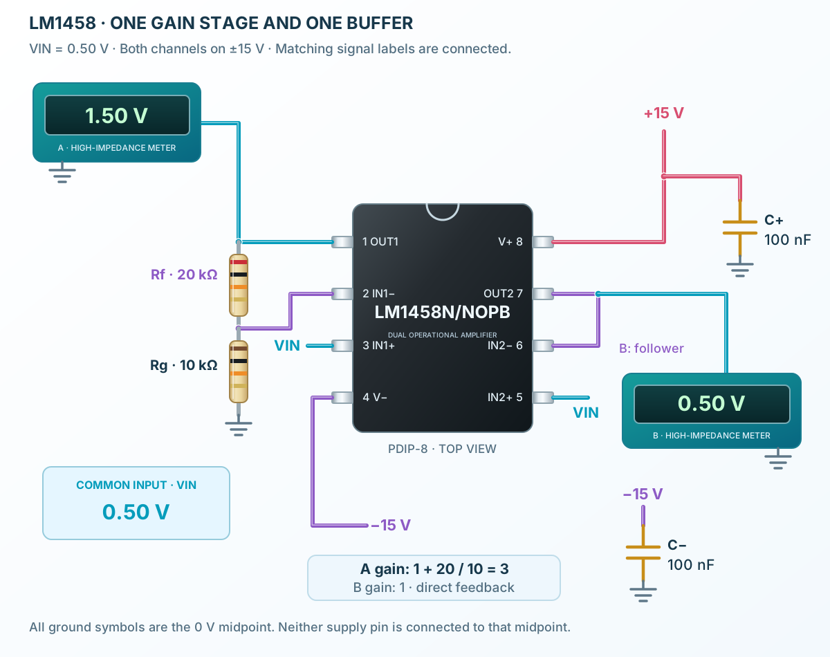
Two compensated input-to-output paths inside one eight-pin IC.
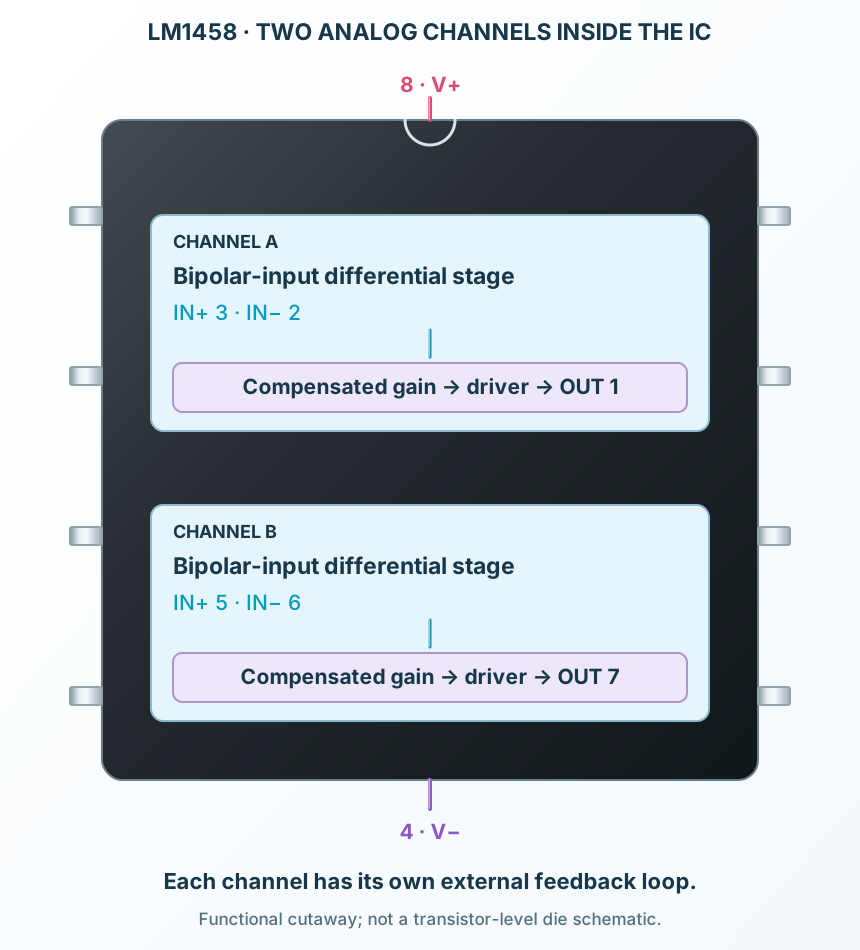
Explore the circuit
Select a stage to see its role and connections
Input stages
Each bipolar differential input pair compares the applied signal against its feedback voltage. Input bias currents flowing in source and feedback resistances introduce additional voltage error.
Gain and compensation
Each channel has an internal voltage-gain path and frequency compensation.
Output drivers
The output stage drives the feedback network and load. Neither input common-mode range nor output swing reaches the rails. Short-circuit protection is a fault feature, not a useful load-current specification.
Selected packagePDIP-8LM1458N/NOPB
Physical connections8 pinsPackage-specific numbering
Reference collection7 tables37 parameters & pin functions
Pin reference
Signal names, electrical functions and connection guidance
Physical pin numbers8 pins
Scroll within the table to see all columns and rows.
| Pin | Signal | Type | Function & connection |
|---|---|---|---|
| OUT1 | Analog output | Channel A output.Connection guidanceReturn to IN1− through 20 kΩ; connect a high-impedance meter. | |
| IN1− | Inverting input | Channel A negative-feedback node.Connection guidanceJoin 20 kΩ from OUT1 and 10 kΩ to signal ground. | |
| IN1+ | Non-inverting input | Channel A signal input.Connection guidanceApply VIN = 0.50 V relative to the 0 V midpoint. | |
| V− | Negative supply | Negative rail shared by both amplifiers.Connection guidanceConnect −15 V; bypass locally to 0 V with 100 nF. | |
| IN2+ | Non-inverting input | Channel B signal input.Connection guidanceConnect to the same VIN in the illustrated follower. | |
| IN2− | Inverting input | Channel B feedback input.Connection guidanceConnect directly to OUT2 pin 7. | |
| OUT2 | Analog output | Channel B output.Connection guidanceConnect to IN2−; leave unloaded or use a high-impedance instrument. | |
| V+ | Positive supply | Positive rail shared by both amplifiers.Connection guidanceConnect +15 V; bypass locally to 0 V with 100 nF. |
No pins match these filters. Try another signal name or reset the filters.
Operating conditions and stress limits
LM1458 commercial grade
Manufacturer-referenced values7 parameters
Scroll within the table to see all columns and rows.
| Parameter | Value | Conditions / notes |
|---|---|---|
| Specified ambient range | 0 to +70°C | LM1458, not LM1558 |
| Electrical-characterization supply | ±15 V | The example follows this test condition |
| Absolute maximum supply | ±18 V | Stress limit, not an operating recommendation |
| Absolute differential input | ±30 V | Respect input and supply conditions |
| Absolute input voltage | ±15 V | At lower supply voltages, do not exceed either supply rail |
| Maximum junction temperature | 100°C | LM1458 rating |
| PDIP power dissipation limit | 400 mW | Derate using the manufacturer guidance and actual mounting |
No specifications match. Try a parameter name or a unit.
This legacy document does not provide a separate recommended minimum supply. No unverified low-voltage range is inferred.
Input accuracy and bias current
±15 V · 25°C unless stated
Manufacturer-referenced values5 parameters
Scroll within the table to see all columns and rows.
| Parameter | Value | Conditions / notes |
|---|---|---|
| Input offset voltage | 1 mV typical; 6 mV maximum | RS ≤10 kΩ; 7.5 mV maximum over temperature |
| Input offset current | 80 nA typical; 200 nA maximum | 300 nA maximum over temperature |
| Input bias current | 200 nA typical; 500 nA maximum | 0.8 µA maximum over temperature |
| Input resistance | 0.3 MΩ minimum; 1 MΩ typical | 25°C characterization |
| Total supply current | 3 mA typical; 5.6 mA maximum | Both amplifiers; ±15 V; 25°C |
No specifications match. Try a parameter name or a unit.
Choose source and feedback resistances with input-current error in mind.
Gain, common mode and output swing
±15 V rails; respect load conditions
Manufacturer-referenced values6 parameters
Scroll within the table to see all columns and rows.
| Parameter | Value | Conditions / notes |
|---|---|---|
| Large-signal open-loop gain at 25°C | 20 V/mV minimum; 160 V/mV typical | VO=±10 V; RL≥2 kΩ |
| Open-loop gain over temperature | 15 V/mV minimum | Same output and load condition |
| Input common-mode range | ±12 V minimum | Within ±15 V rails |
| Output swing at RL≥10 kΩ | ±12 V minimum; ±14 V typical | Light-load swing |
| Output swing at RL≥2 kΩ | ±10 V minimum; ±13 V typical | Heavier loading reduces headroom |
| Example output range | 1.50 V and 0.50 V nominal | Light DC loads; well inside the specified swing |
No specifications match. Try a parameter name or a unit.
Typical output headroom is not a guaranteed limit.
Rejection, stability and practical limits
Use the source document’s actual guarantees
Manufacturer-referenced values7 parameters
Scroll within the table to see all columns and rows.
| Parameter | Value | Conditions / notes |
|---|---|---|
| Common-mode rejection | 70 dB minimum; 90 dB typical | RS≤10 kΩ |
| Supply-voltage rejection | 77 dB minimum; 96 dB typical | RS≤10 kΩ |
| Frequency compensation | Internal | No external compensation required |
| Supply bypass | 100 nF from each rail to 0 V | Local bypass; add bulk decoupling as needed |
| PDIP junction-to-ambient estimate | 187°C/W | Manufacturer package estimate; mounting dependent |
| Short-circuit protection | Included | Check dissipation; do not use a short as a normal load |
| Bandwidth, slew rate and noise | No numeric claim on this page | Not specified in the selected manufacturer electrical table |
No specifications match. Try a parameter name or a unit.
The 0 V signal midpoint is distinct from the negative supply pin.
Two-channel amplifier example
±15 V rails · 0 V signal reference
Manufacturer-referenced values7 parameters
Scroll within the table to see all columns and rows.
| Parameter | Value | Conditions / notes |
|---|---|---|
| Input VIN | 0.50 V | Pins 3 and 5; common signal ground |
| Channel A feedback | 20 kΩ | OUT1 pin 1 to IN1− pin 2 |
| Channel A ground resistor | 10 kΩ | IN1− pin 2 to 0 V |
| Channel A ideal output | 1.50 V | 0.50 × (1 + 20 / 10) |
| Channel B feedback | Direct connection | OUT2 pin 7 to IN2− pin 6 |
| Channel B ideal output | 0.50 V | Unity-gain follower |
| Bypass capacitors | 100 nF per rail | Each supply rail to the 0 V midpoint |
No specifications match. Try a parameter name or a unit.
The 0 V reference is not the negative supply pin. Keep both rail-bypass loops short.
Physical pin reference
LM1458N/NOPB · PDIP-8
Manufacturer-referenced values5 parameters
Scroll within the table to see all columns and rows.
| Parameter | Value | Conditions / notes |
|---|---|---|
| Lead pitch | 2.54 mm | Through-hole |
| Channel A | OUT1 1; IN1− 2; IN1+ 3 | Independent feedback loop |
| Channel B | IN2+ 5; IN2− 6; OUT2 7 | Independent feedback loop |
| Supply | V− 4; V+ 8 | Shared by both channels |
| Package orientation | Top view; pin 1 at the marker | Counterclockwise numbering |
No specifications match. Try a parameter name or a unit.
This dual-amplifier pinout differs from single amplifiers such as TL081 or LM741.
No matching rowsTry a pin name, parameter, unit or test condition, or reset the filters.
Low-frequency analog gain
Use controlled negative feedback for signals whose headroom and accuracy requirements fit the device.
Manufacturer application guideAnalog buffers
Buffer moderate-impedance signals into compatible light loads; include input bias-current error.
Manufacturer application guideEducational dual-amplifier circuits
Compare an amplified channel with a follower while observing independent feedback on shared supplies.
Manufacturer application guideTake it into ProTech
Find LM1458 in the Components Library to place its schematic symbol and connect its pins.
Reference page · circuit simulation model not yet availableOpen ProTech