Real View
Two fast threshold decisions, with independently returned output stages.
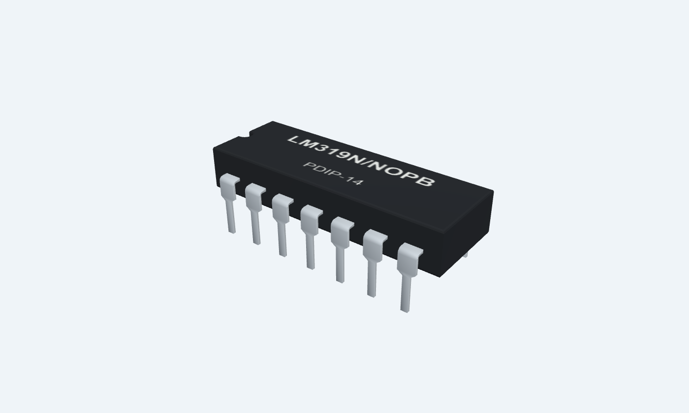
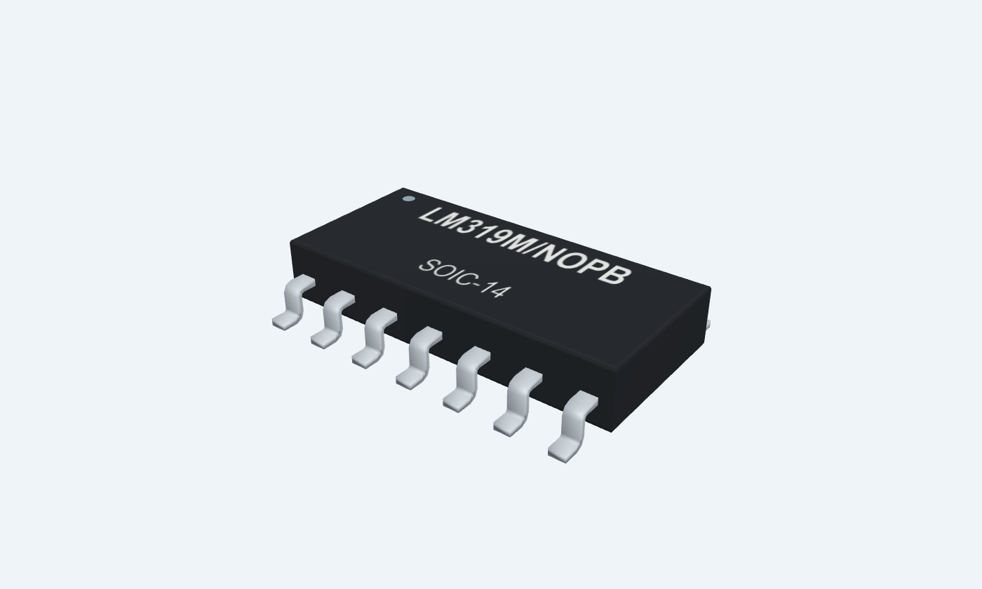
LM319 contains two high-speed voltage comparators. Each compares an input pair and controls an open-collector output, allowing the pull-up supply and output-stage return to be chosen within the device limits. It makes threshold decisions rather than providing linear op-amp gain. This page selects TI LM319N/NOPB in PDIP-14 and LM319M/NOPB in SOIC-14, both commercial 0–70°C parts. Four physical pins are unconnected. The fourteen-pin drawing defines the mapping; it must not be confused with the family’s ten-pin metal-can arrangement. The example uses a 5 V supply, a 2 V divider reference and a 1.5 V input. A 10 kΩ pull-up lets the first output indicate LOW or HIGH. Both inputs stay in the 1–3 V common-mode range; the second comparator is also given defined inputs. The quoted 80 ns response is typical under ±15 V test conditions, not a speed guarantee for this 5 V example.
Select a pin to explore its connection
Click a lead or use the arrow keys. Top view
No internal connection for the selected fourteen-pin package.
Leave open; do not connect to ground.
No internal connection for the selected fourteen-pin package.
Leave open; do not connect to ground.
Emitter return for comparator 1 output transistor.
Connect to the common 0 V return in this example.
Separate from the analog negative supply pin; observe every rail-to-ground rating.
Positive input for comparator 1.
Apply VIN = 1.50 V.
At a 5 V supply both inputs must remain between 1 V and 3 V.
Threshold input for comparator 1.
Connect the 2.00 V reference.
Input polarity controls the open-collector state.
Negative supply for both comparator input/gain paths.
Connect to 0 V in the shown single-supply circuit.
In split-supply use this can differ from the output-stage returns.
Sinks current when IN+ is lower than IN−; releases when IN+ is higher.
Leave unused output open in the illustrated circuit.
No internal high-level driver; external pull-up is required to observe HIGH.
Emitter return for comparator 2 output transistor.
Connect to the common 0 V return in this example.
Separate from the analog negative supply pin; observe every rail-to-ground rating.
Positive input for comparator 2.
Tie to the same 1.50 V VIN node.
At a 5 V supply both inputs must remain between 1 V and 3 V.
Threshold input for comparator 2.
Connect the 2.00 V reference.
Input polarity controls the open-collector state.
Positive supply shared by both comparators.
Connect regulated +5 V and bypass locally with 100 nF to pin 6.
Sinks current when IN+ is lower than IN−; releases when IN+ is higher.
Add a 10 kΩ pull-up to +5 V and a high-impedance meter.
No internal high-level driver; external pull-up is required to observe HIGH.
No internal connection for the selected fourteen-pin package.
Leave open; do not connect to ground.
No internal connection for the selected fourteen-pin package.
Leave open; do not connect to ground.
The output transistor pulls LOW or releases the line. A separate external resistor creates HIGH; the IC does not actively source that state.
LM319N/NOPB · PDIP-14
| Property | Details |
|---|---|
| Manufacturer | Texas Instruments |
| Part number | LM319N/NOPB |
| Package | PDIP-14 |
| Connections | 14 pins |
| Mounting | Through-hole |
| Lead pitch | 2.54 mm |
| Package code | dip |
| Thermal reference | Board and package dependent; see manufacturer data |
Selected TI LM319, not the A-grade column
Scroll sideways to see all columns.
| Parameter | Value | Conditions / notes |
|---|---|---|
| Supply capability | Single 5 V through ±15 V | Electrical-section applicability; observe all ground-relative limits |
| Illustrated rails | V+ = 5 V; V− = 0 V | Pin 11 positive; pin 6 negative |
| Input range at 5 V | 1–3 V | Ground is outside the specified input range |
| Input range at ±15 V | ±13 V typical | Manufacturer electrical table |
| Ambient operating range | 0–70°C | LM319N/M commercial orders |
| Ground-to-supply operating note | Do not exceed 16 V | Manufacturer electrical-section instruction |
No specifications match. Try a parameter name or a unit.
Recommended operating conditions and absolute stress limits are distinct.
±15 V; 25°C unless noted
Scroll sideways to see all columns.
| Parameter | Value | Conditions / notes |
|---|---|---|
| Input offset | 2 mV typical; 8 mV maximum | RS ≤ 5 kΩ |
| Offset over temperature | 10 mV maximum | 0–70°C; RS ≤ 5 kΩ |
| Input bias current | 250 nA typical; 1000 nA maximum | 1200 nA maximum over temperature |
| Input offset current | 80 nA typical; 200 nA maximum | 300 nA maximum over temperature |
| Voltage gain | 8 V/mV minimum; 40 V/mV typical | Output pulled to 15 V through 1.4 kΩ |
No specifications match. Try a parameter name or a unit.
Offset specifications use the manufacturer output/load definition; do not treat typical values as guarantees.
Retain the test conditions
Scroll sideways to see all columns.
| Parameter | Value | Conditions / notes |
|---|---|---|
| Response time | 80 ns typical | ±15 V; 100 mV step with 5 mV overdrive |
| Saturation at 25 mA | 0.75 V typical; 1.5 V maximum | VIN differential ≤ −10 mV; 25°C |
| Saturation at ≤3.2 mA | 0.3 V typical; 0.4 V maximum | V+ ≥ 4.5 V, V− = 0 V; differential ≤ −10 mV |
| Output leakage | 0.2 µA typical; 10 µA maximum | 35 V output, 25°C; V− and GND = 0 V; differential ≥ 10 mV |
| Pull-up rise time | Depends on resistance and capacitance | Do not equate the 80 ns figure with every circuit edge |
No specifications match. Try a parameter name or a unit.
A 10 kΩ pull-up is suitable for this low-current DC illustration, not a promise of maximum switching speed.
Check every voltage reference
Scroll sideways to see all columns.
| Parameter | Value | Conditions / notes |
|---|---|---|
| Positive supply current at 5 V | 4.3 mA typical | 25°C; V− = 0 V |
| Positive supply current at ±15 V | 8 mA typical; 12.5 mA maximum | 25°C |
| Negative supply current at ±15 V | 3 mA typical; 5 mA maximum | 25°C |
| Absolute total supply | 36 V | Stress limit |
| Absolute differential input | ±5 V | Do not apply supply-span differential signals |
| Absolute output to V− | 36 V | Collector stress limit |
| Absolute GND to V− / V+ | 25 V / 18 V | Separate output-stage return constraints |
| Absolute power dissipation | 500 mW | Thermal conditions and derating still apply |
No specifications match. Try a parameter name or a unit.
Absolute limits do not authorize continuous operation at those conditions.
Calculated DC example, not a timing simulation
Scroll sideways to see all columns.
| Parameter | Value | Conditions / notes |
|---|---|---|
| Reference divider | 30 kΩ upper; 20 kΩ lower | 5 × 20/(30+20) = 2.00 V, before input-current error |
| VIN = 1.50 V | OUT1 LOW | Input 4 below reference input 5 |
| VIN = 2.50 V | OUT1 released / HIGH | External pull-up creates high level |
| Pull-up | 10 kΩ to +5 V | Connected to output pin 12 |
| Illustrative LOW current | About 0.47 mA | (5−0.3)/10 kΩ; 0.3 V is a typical estimate |
| Second comparator | IN+9 = VIN; IN−10 = VREF | Output 7 left unused |
| Local bypass | 100 nF between pins 11 and 6 | All GND symbols in this example share 0 V |
No specifications match. Try a parameter name or a unit.
Input bias loads the divider; use a lower source impedance or buffer when threshold accuracy matters.
LM319N/NOPB · PDIP-14
Scroll sideways to see all columns.
| Parameter | Value | Conditions / notes |
|---|---|---|
| Lead pitch | 2.54 mm | Through-hole |
| Channel 1 | 4 IN+; 5 IN−; 12 OUT | Output-stage return: pin 3 |
| Channel 2 | 9 IN+; 10 IN−; 7 OUT | Output-stage return: pin 8 |
| Analog supplies | 11 V+; 6 V− | Shared by both channels |
| No connection | 1, 2, 13, 14 | Leave open |
| Pin-map source | TI fourteen-pin drawing, page 3 | Cross-checked against ST fourteen-pin drawing |
| Layout | Short bypass and output-current loops | Keep output switching currents away from input/reference traces |
No specifications match. Try a parameter name or a unit.
Use the package drawing: the TI pin-function table has inconsistent ten/fourteen-pin column labels.
Select a pin for its function, connection guidance and electrical notes.
Follow the labeled connections and functional stages
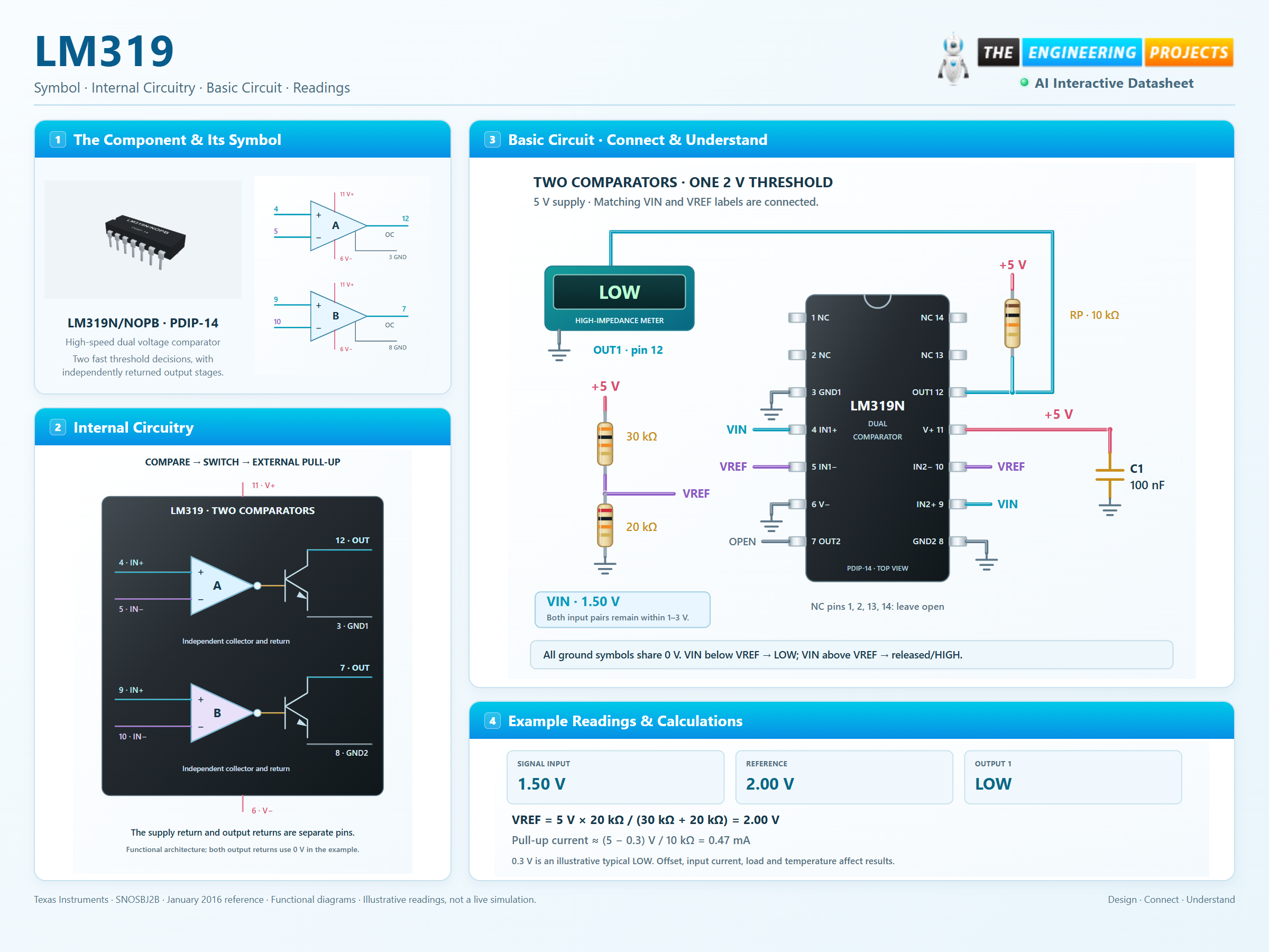
3 stages · Explore one step at a time
30 kΩ above 20 kΩ creates an ideal 2 V reference from 5 V. Both input voltages must remain between 1 V and 3 V.
Channel 1 compares VIN at pin 4 with VREF at pin 5. VIN below VREF turns its output transistor on.
The 10 kΩ pull-up on pin 12 creates HIGH when the transistor turns off. Pins 3 and 8 return output current to 0 V.
A physical fourteen-pin IC, divider and pulled-up collector.
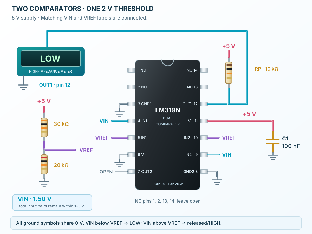
Follow the component values and pin connections
Connect 11 to +5 V; connect 6, 3 and 8 to 0 V; bypass the analog supply.
Connect VIN to 4 and 9, and VREF to 5 and 10.
Read output 12 through its 10 kΩ pull-up. Keep output 7 and all NC pins open.
Two comparators with separate output-transistor returns.
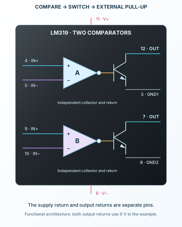
Select a stage to see its role and connections
Each differential input pair controls one independent comparison.
A gain path switches the collector transistor on or off.
Each output transistor has its own return pin; both are grounded in this example.
Signal names, electrical functions and connection guidance
Scroll within the table to see all columns and rows.
| Pin | Signal | Type | Function & connection |
|---|---|---|---|
| NC | No connection | No internal connection for the selected fourteen-pin package.Connection guidanceLeave open; do not connect to ground. | |
| NC | No connection | No internal connection for the selected fourteen-pin package.Connection guidanceLeave open; do not connect to ground. | |
| GND1 | Output-stage return | Emitter return for comparator 1 output transistor.Connection guidanceConnect to the common 0 V return in this example. Separate from the analog negative supply pin; observe every rail-to-ground rating. | |
| IN1+ | Non-inverting input | Positive input for comparator 1.Connection guidanceApply VIN = 1.50 V. At a 5 V supply both inputs must remain between 1 V and 3 V. | |
| IN1− | Inverting input | Threshold input for comparator 1.Connection guidanceConnect the 2.00 V reference. Input polarity controls the open-collector state. | |
| V− | Negative analog supply | Negative supply for both comparator input/gain paths.Connection guidanceConnect to 0 V in the shown single-supply circuit. In split-supply use this can differ from the output-stage returns. | |
| OUT2 | Open-collector output | Sinks current when IN+ is lower than IN−; releases when IN+ is higher.Connection guidanceLeave unused output open in the illustrated circuit. No internal high-level driver; external pull-up is required to observe HIGH. | |
| GND2 | Output-stage return | Emitter return for comparator 2 output transistor.Connection guidanceConnect to the common 0 V return in this example. Separate from the analog negative supply pin; observe every rail-to-ground rating. | |
| IN2+ | Non-inverting input | Positive input for comparator 2.Connection guidanceTie to the same 1.50 V VIN node. At a 5 V supply both inputs must remain between 1 V and 3 V. | |
| IN2− | Inverting input | Threshold input for comparator 2.Connection guidanceConnect the 2.00 V reference. Input polarity controls the open-collector state. | |
| V+ | Positive analog supply | Positive supply shared by both comparators.Connection guidanceConnect regulated +5 V and bypass locally with 100 nF to pin 6. | |
| OUT1 | Open-collector output | Sinks current when IN+ is lower than IN−; releases when IN+ is higher.Connection guidanceAdd a 10 kΩ pull-up to +5 V and a high-impedance meter. No internal high-level driver; external pull-up is required to observe HIGH. | |
| NC | No connection | No internal connection for the selected fourteen-pin package.Connection guidanceLeave open; do not connect to ground. | |
| NC | No connection | No internal connection for the selected fourteen-pin package.Connection guidanceLeave open; do not connect to ground. |
No pins match these filters. Try another signal name or reset the filters.
Selected TI LM319, not the A-grade column
Scroll within the table to see all columns and rows.
| Parameter | Value | Conditions / notes |
|---|---|---|
| Supply capability | Single 5 V through ±15 V | Electrical-section applicability; observe all ground-relative limits |
| Illustrated rails | V+ = 5 V; V− = 0 V | Pin 11 positive; pin 6 negative |
| Input range at 5 V | 1–3 V | Ground is outside the specified input range |
| Input range at ±15 V | ±13 V typical | Manufacturer electrical table |
| Ambient operating range | 0–70°C | LM319N/M commercial orders |
| Ground-to-supply operating note | Do not exceed 16 V | Manufacturer electrical-section instruction |
No specifications match. Try a parameter name or a unit.
Recommended operating conditions and absolute stress limits are distinct.
±15 V; 25°C unless noted
Scroll within the table to see all columns and rows.
| Parameter | Value | Conditions / notes |
|---|---|---|
| Input offset | 2 mV typical; 8 mV maximum | RS ≤ 5 kΩ |
| Offset over temperature | 10 mV maximum | 0–70°C; RS ≤ 5 kΩ |
| Input bias current | 250 nA typical; 1000 nA maximum | 1200 nA maximum over temperature |
| Input offset current | 80 nA typical; 200 nA maximum | 300 nA maximum over temperature |
| Voltage gain | 8 V/mV minimum; 40 V/mV typical | Output pulled to 15 V through 1.4 kΩ |
No specifications match. Try a parameter name or a unit.
Offset specifications use the manufacturer output/load definition; do not treat typical values as guarantees.
Retain the test conditions
Scroll within the table to see all columns and rows.
| Parameter | Value | Conditions / notes |
|---|---|---|
| Response time | 80 ns typical | ±15 V; 100 mV step with 5 mV overdrive |
| Saturation at 25 mA | 0.75 V typical; 1.5 V maximum | VIN differential ≤ −10 mV; 25°C |
| Saturation at ≤3.2 mA | 0.3 V typical; 0.4 V maximum | V+ ≥ 4.5 V, V− = 0 V; differential ≤ −10 mV |
| Output leakage | 0.2 µA typical; 10 µA maximum | 35 V output, 25°C; V− and GND = 0 V; differential ≥ 10 mV |
| Pull-up rise time | Depends on resistance and capacitance | Do not equate the 80 ns figure with every circuit edge |
No specifications match. Try a parameter name or a unit.
A 10 kΩ pull-up is suitable for this low-current DC illustration, not a promise of maximum switching speed.
Check every voltage reference
Scroll within the table to see all columns and rows.
| Parameter | Value | Conditions / notes |
|---|---|---|
| Positive supply current at 5 V | 4.3 mA typical | 25°C; V− = 0 V |
| Positive supply current at ±15 V | 8 mA typical; 12.5 mA maximum | 25°C |
| Negative supply current at ±15 V | 3 mA typical; 5 mA maximum | 25°C |
| Absolute total supply | 36 V | Stress limit |
| Absolute differential input | ±5 V | Do not apply supply-span differential signals |
| Absolute output to V− | 36 V | Collector stress limit |
| Absolute GND to V− / V+ | 25 V / 18 V | Separate output-stage return constraints |
| Absolute power dissipation | 500 mW | Thermal conditions and derating still apply |
No specifications match. Try a parameter name or a unit.
Absolute limits do not authorize continuous operation at those conditions.
Calculated DC example, not a timing simulation
Scroll within the table to see all columns and rows.
| Parameter | Value | Conditions / notes |
|---|---|---|
| Reference divider | 30 kΩ upper; 20 kΩ lower | 5 × 20/(30+20) = 2.00 V, before input-current error |
| VIN = 1.50 V | OUT1 LOW | Input 4 below reference input 5 |
| VIN = 2.50 V | OUT1 released / HIGH | External pull-up creates high level |
| Pull-up | 10 kΩ to +5 V | Connected to output pin 12 |
| Illustrative LOW current | About 0.47 mA | (5−0.3)/10 kΩ; 0.3 V is a typical estimate |
| Second comparator | IN+9 = VIN; IN−10 = VREF | Output 7 left unused |
| Local bypass | 100 nF between pins 11 and 6 | All GND symbols in this example share 0 V |
No specifications match. Try a parameter name or a unit.
Input bias loads the divider; use a lower source impedance or buffer when threshold accuracy matters.
LM319N/NOPB · PDIP-14
Scroll within the table to see all columns and rows.
| Parameter | Value | Conditions / notes |
|---|---|---|
| Lead pitch | 2.54 mm | Through-hole |
| Channel 1 | 4 IN+; 5 IN−; 12 OUT | Output-stage return: pin 3 |
| Channel 2 | 9 IN+; 10 IN−; 7 OUT | Output-stage return: pin 8 |
| Analog supplies | 11 V+; 6 V− | Shared by both channels |
| No connection | 1, 2, 13, 14 | Leave open |
| Pin-map source | TI fourteen-pin drawing, page 3 | Cross-checked against ST fourteen-pin drawing |
| Layout | Short bypass and output-current loops | Keep output switching currents away from input/reference traces |
No specifications match. Try a parameter name or a unit.
Use the package drawing: the TI pin-function table has inconsistent ten/fourteen-pin column labels.
No matching rowsTry a pin name, parameter, unit or test condition, or reset the filters.
Compare a compatible input against a reference, allowing for offset and noise.
Manufacturer application guideUse the two channels for upper and lower limits with appropriate output logic.
Manufacturer application guideUse external collector pull-ups and output returns within the specified ratings.
Manufacturer application guideFind LM319 in the Components Library to place its schematic symbol and connect its pins.
Reference page · circuit simulation model not yet availableOpen ProTech