LM319High-speed dual voltage comparator
Two fast threshold decisions, with independently returned output stages.
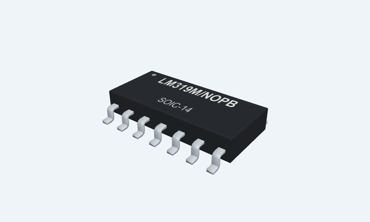
LM319 contains two high-speed voltage comparators. Each compares an input pair and controls an open-collector output, allowing the pull-up supply and output-stage return to be chosen within the device limits. It makes threshold decisions rather than providing linear op-amp gain. This page selects TI LM319N/NOPB in PDIP-14 and LM319M/NOPB in SOIC-14, both commercial 0–70°C parts. Four physical pins are unconnected. The fourteen-pin drawing defines the mapping; it must not be confused with the family’s ten-pin metal-can arrangement. The example uses a 5 V supply, a 2 V divider reference and a 1.5 V input. A 10 kΩ pull-up lets the first output indicate LOW or HIGH. Both inputs stay in the 1–3 V common-mode range; the second comparator is also given defined inputs. The quoted 80 ns response is typical under ±15 V test conditions, not a speed guarantee for this 5 V example.

14Physical pins
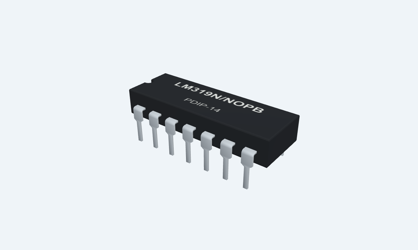
LM319N/NOPBPDIP-14
Manufacturer-referencedTexas Instruments
Pin diagram
Select a pin to explore its connection
Highlight
LM319PDIP-14Top view
LM319SOIC-14Top view
Click a lead or use the arrow keys. Top view
PIN 1 · Not connected
No connectionNC
Function
No internal connection for the selected fourteen-pin package.
How to connect
Leave open; do not connect to ground.
PIN 2 · Not connected
No connectionNC
Function
No internal connection for the selected fourteen-pin package.
How to connect
Leave open; do not connect to ground.
PIN 3 · Supply
Output-stage returnGND1
Function
Emitter return for comparator 1 output transistor.
How to connect
Connect to the common 0 V return in this example.
Electrical note
Separate from the analog negative supply pin; observe every rail-to-ground rating.
PIN 4 · Comparator inputs
Non-inverting inputIN1+
Function
Positive input for comparator 1.
How to connect
Apply VIN = 1.50 V.
Electrical note
At a 5 V supply both inputs must remain between 1 V and 3 V.
PIN 5 · Comparator inputs
Inverting inputIN1−
Function
Threshold input for comparator 1.
How to connect
Connect the 2.00 V reference.
Electrical note
Input polarity controls the open-collector state.
PIN 6 · Supply
Negative analog supplyV−
Function
Negative supply for both comparator input/gain paths.
How to connect
Connect to 0 V in the shown single-supply circuit.
Electrical note
In split-supply use this can differ from the output-stage returns.
PIN 7 · Open collectors
Open-collector outputOUT2
Function
Sinks current when IN+ is lower than IN−; releases when IN+ is higher.
How to connect
Leave unused output open in the illustrated circuit.
Electrical note
No internal high-level driver; external pull-up is required to observe HIGH.
PIN 8 · Supply
Output-stage returnGND2
Function
Emitter return for comparator 2 output transistor.
How to connect
Connect to the common 0 V return in this example.
Electrical note
Separate from the analog negative supply pin; observe every rail-to-ground rating.
PIN 9 · Comparator inputs
Non-inverting inputIN2+
Function
Positive input for comparator 2.
How to connect
Tie to the same 1.50 V VIN node.
Electrical note
At a 5 V supply both inputs must remain between 1 V and 3 V.
PIN 10 · Comparator inputs
Inverting inputIN2−
Function
Threshold input for comparator 2.
How to connect
Connect the 2.00 V reference.
Electrical note
Input polarity controls the open-collector state.
PIN 11 · Supply
Positive analog supplyV+
Function
Positive supply shared by both comparators.
How to connect
Connect regulated +5 V and bypass locally with 100 nF to pin 6.
PIN 12 · Open collectors
Open-collector outputOUT1
Function
Sinks current when IN+ is lower than IN−; releases when IN+ is higher.
How to connect
Add a 10 kΩ pull-up to +5 V and a high-impedance meter.
Electrical note
No internal high-level driver; external pull-up is required to observe HIGH.
PIN 13 · Not connected
No connectionNC
Function
No internal connection for the selected fourteen-pin package.
How to connect
Leave open; do not connect to ground.
PIN 14 · Not connected
No connectionNC
Function
No internal connection for the selected fourteen-pin package.
How to connect
Leave open; do not connect to ground.
Key specifications
The output transistor pulls LOW or releases the line. A separate external resistor creates HIGH; the IC does not actively source that state.
Independent comparators2 Separate output-stage returns
Typical response80 ns · ±15 V test
Illustrated supply5 V · inputs kept at 1–3 V
Selected ambient range0–70 °C
Package details
LM319N/NOPB · PDIP-14
| Property | Details |
|---|---|
| Manufacturer | Texas Instruments |
| Part number | LM319N/NOPB |
| Package | PDIP-14 |
| Connections | 14 pins |
| Mounting | Through-hole |
| Lead pitch | 2.54 mm |
| Package code | dip |
| Thermal reference | Board and package dependent; see manufacturer data |
Supply and input conditions
Selected TI LM319, not the A-grade column
Manufacturer specifications 6 parameters
Scroll sideways to see all columns.
| Parameter | Value | Conditions / notes |
|---|---|---|
| Supply capability | Single 5 V through ±15 V | Electrical-section applicability; observe all ground-relative limits |
| Illustrated rails | V+ = 5 V; V− = 0 V | Pin 11 positive; pin 6 negative |
| Input range at 5 V | 1–3 V | Ground is outside the specified input range |
| Input range at ±15 V | ±13 V typical | Manufacturer electrical table |
| Ambient operating range | 0–70°C | LM319N/M commercial orders |
| Ground-to-supply operating note | Do not exceed 16 V | Manufacturer electrical-section instruction |
No specifications match. Try a parameter name or a unit.
Recommended operating conditions and absolute stress limits are distinct.
Input accuracy and current
±15 V; 25°C unless noted
Manufacturer specifications 5 parameters
Scroll sideways to see all columns.
| Parameter | Value | Conditions / notes |
|---|---|---|
| Input offset | 2 mV typical; 8 mV maximum | RS ≤ 5 kΩ |
| Offset over temperature | 10 mV maximum | 0–70°C; RS ≤ 5 kΩ |
| Input bias current | 250 nA typical; 1000 nA maximum | 1200 nA maximum over temperature |
| Input offset current | 80 nA typical; 200 nA maximum | 300 nA maximum over temperature |
| Voltage gain | 8 V/mV minimum; 40 V/mV typical | Output pulled to 15 V through 1.4 kΩ |
No specifications match. Try a parameter name or a unit.
Offset specifications use the manufacturer output/load definition; do not treat typical values as guarantees.
Response and open-collector output
Retain the test conditions
Manufacturer specifications 5 parameters
Scroll sideways to see all columns.
| Parameter | Value | Conditions / notes |
|---|---|---|
| Response time | 80 ns typical | ±15 V; 100 mV step with 5 mV overdrive |
| Saturation at 25 mA | 0.75 V typical; 1.5 V maximum | VIN differential ≤ −10 mV; 25°C |
| Saturation at ≤3.2 mA | 0.3 V typical; 0.4 V maximum | V+ ≥ 4.5 V, V− = 0 V; differential ≤ −10 mV |
| Output leakage | 0.2 µA typical; 10 µA maximum | 35 V output, 25°C; V− and GND = 0 V; differential ≥ 10 mV |
| Pull-up rise time | Depends on resistance and capacitance | Do not equate the 80 ns figure with every circuit edge |
No specifications match. Try a parameter name or a unit.
A 10 kΩ pull-up is suitable for this low-current DC illustration, not a promise of maximum switching speed.
Power and stress limits
Check every voltage reference
Manufacturer specifications 8 parameters
Scroll sideways to see all columns.
| Parameter | Value | Conditions / notes |
|---|---|---|
| Positive supply current at 5 V | 4.3 mA typical | 25°C; V− = 0 V |
| Positive supply current at ±15 V | 8 mA typical; 12.5 mA maximum | 25°C |
| Negative supply current at ±15 V | 3 mA typical; 5 mA maximum | 25°C |
| Absolute total supply | 36 V | Stress limit |
| Absolute differential input | ±5 V | Do not apply supply-span differential signals |
| Absolute output to V− | 36 V | Collector stress limit |
| Absolute GND to V− / V+ | 25 V / 18 V | Separate output-stage return constraints |
| Absolute power dissipation | 500 mW | Thermal conditions and derating still apply |
No specifications match. Try a parameter name or a unit.
Absolute limits do not authorize continuous operation at those conditions.
A 2 V threshold detector
Calculated DC example, not a timing simulation
Manufacturer specifications 7 parameters
Scroll sideways to see all columns.
| Parameter | Value | Conditions / notes |
|---|---|---|
| Reference divider | 30 kΩ upper; 20 kΩ lower | 5 × 20/(30+20) = 2.00 V, before input-current error |
| VIN = 1.50 V | OUT1 LOW | Input 4 below reference input 5 |
| VIN = 2.50 V | OUT1 released / HIGH | External pull-up creates high level |
| Pull-up | 10 kΩ to +5 V | Connected to output pin 12 |
| Illustrative LOW current | About 0.47 mA | (5−0.3)/10 kΩ; 0.3 V is a typical estimate |
| Second comparator | IN+9 = VIN; IN−10 = VREF | Output 7 left unused |
| Local bypass | 100 nF between pins 11 and 6 | All GND symbols in this example share 0 V |
No specifications match. Try a parameter name or a unit.
Input bias loads the divider; use a lower source impedance or buffer when threshold accuracy matters.
Fourteen-pin package map
LM319N/NOPB · PDIP-14
Manufacturer specifications 7 parameters
Scroll sideways to see all columns.
| Parameter | Value | Conditions / notes |
|---|---|---|
| Lead pitch | 2.54 mm | Through-hole |
| Channel 1 | 4 IN+; 5 IN−; 12 OUT | Output-stage return: pin 3 |
| Channel 2 | 9 IN+; 10 IN−; 7 OUT | Output-stage return: pin 8 |
| Analog supplies | 11 V+; 6 V− | Shared by both channels |
| No connection | 1, 2, 13, 14 | Leave open |
| Pin-map source | TI fourteen-pin drawing, page 3 | Cross-checked against ST fourteen-pin drawing |
| Layout | Short bypass and output-current loops | Keep output switching currents away from input/reference traces |
No specifications match. Try a parameter name or a unit.
Use the package drawing: the TI pin-function table has inconsistent ten/fourteen-pin column labels.
Connections by function
Select a pin for its function, connection guidance and electrical notes.
Not connected4 pins
Supply4 pins
Comparator inputs4 pins
Open collectors2 pins
Not connected4 pins
Supply4 pins
Comparator inputs4 pins
Open collectors2 pins
LM319 at a glance
Follow the labeled connections and functional stages
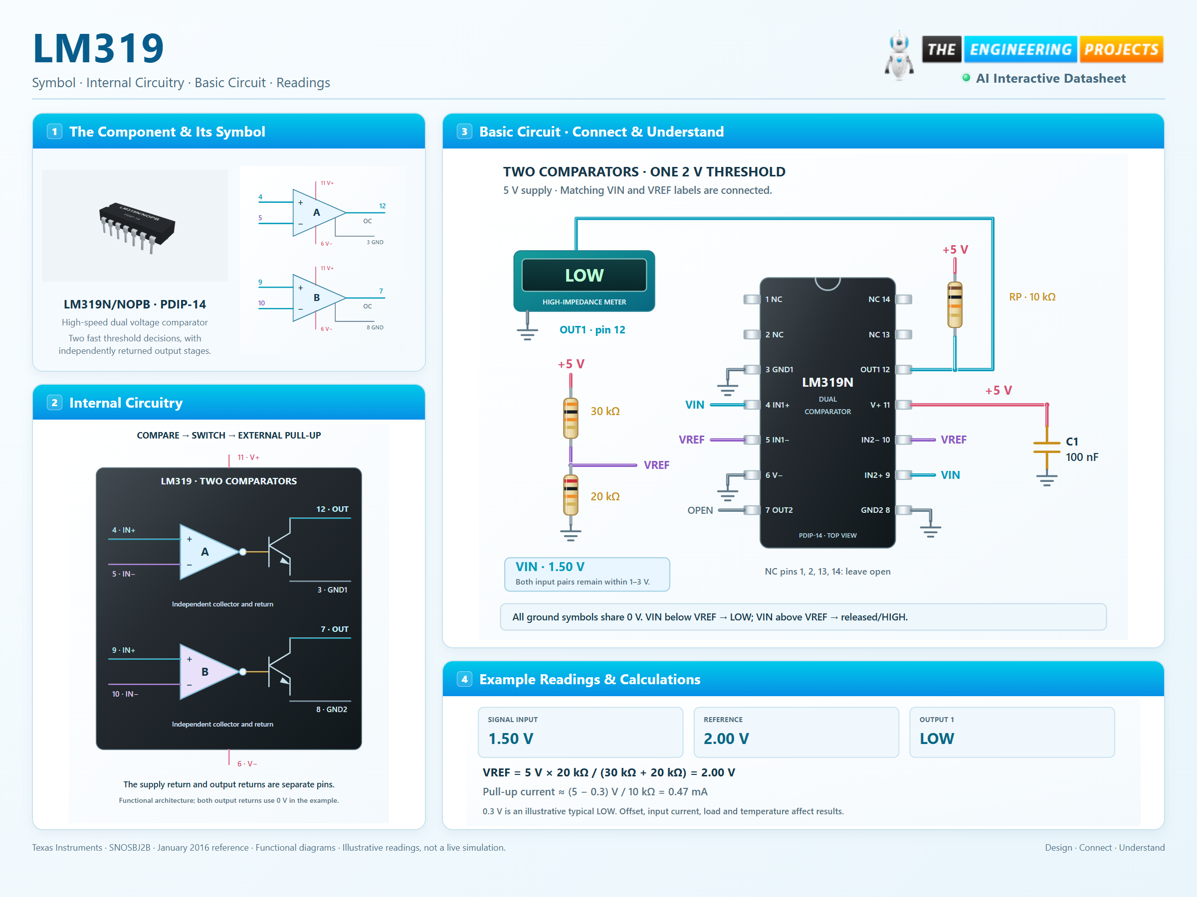
How it works
3 stages · Explore one step at a time
Set a valid threshold
30 kΩ above 20 kΩ creates an ideal 2 V reference from 5 V. Both input voltages must remain between 1 V and 3 V.
Compare the input
Channel 1 compares VIN at pin 4 with VREF at pin 5. VIN below VREF turns its output transistor on.
Read the collector
The 10 kΩ pull-up on pin 12 creates HIGH when the transistor turns off. Pins 3 and 8 return output current to 0 V.
Step 1 of 3
LM319 in a circuit
A physical fourteen-pin IC, divider and pulled-up collector.
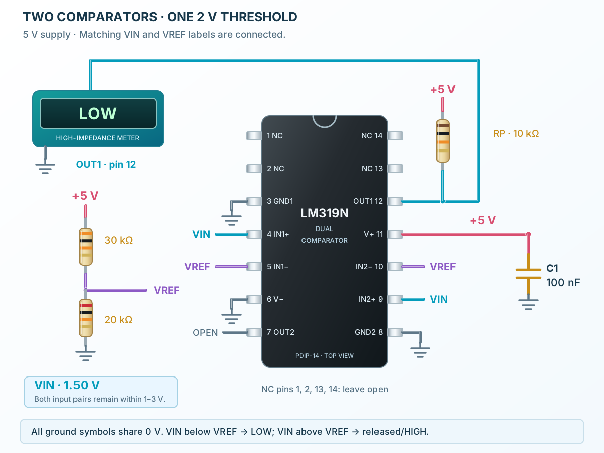
Connect it, step by step
Follow the component values and pin connections
Power
Connect 11 to +5 V; connect 6, 3 and 8 to 0 V; bypass the analog supply.
Compare
Connect VIN to 4 and 9, and VREF to 5 and 10.
Read
Read output 12 through its 10 kΩ pull-up. Keep output 7 and all NC pins open.
Inside LM319
Two comparators with separate output-transistor returns.
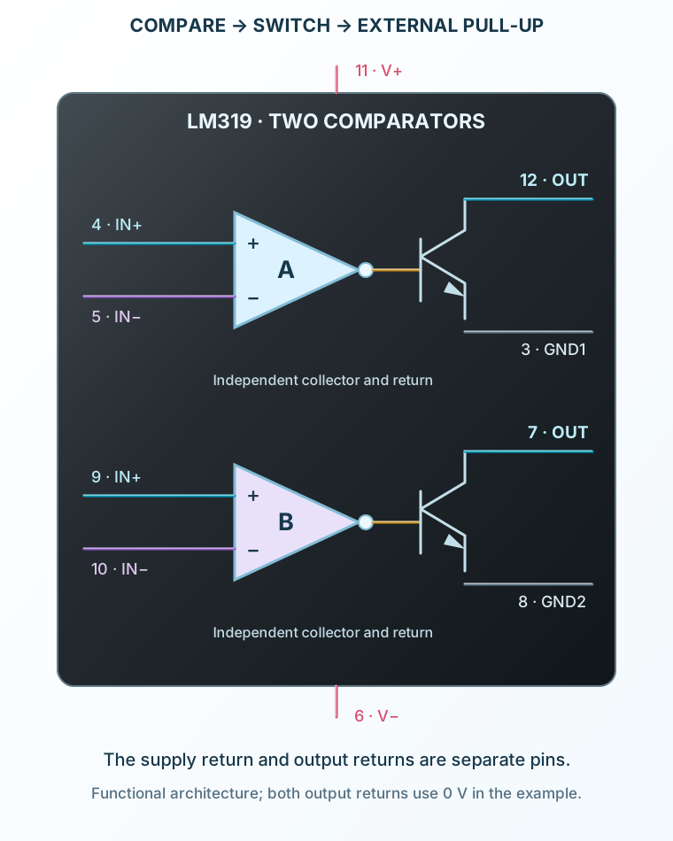
Explore the circuit
Select a stage to see its role and connections
Sense
Each differential input pair controls one independent comparison.
Switch
A gain path switches the collector transistor on or off.
Return current
Each output transistor has its own return pin; both are grounded in this example.
Selected packagePDIP-14LM319N/NOPB
Physical connections14 pinsPackage-specific numbering
Reference collection7 tables38 parameters & pin functions
Pin reference
Signal names, electrical functions and connection guidance
Physical pin numbers14 pins
Scroll within the table to see all columns and rows.
| Pin | Signal | Type | Function & connection |
|---|---|---|---|
| NC | No connection | No internal connection for the selected fourteen-pin package.Connection guidanceLeave open; do not connect to ground. | |
| NC | No connection | No internal connection for the selected fourteen-pin package.Connection guidanceLeave open; do not connect to ground. | |
| GND1 | Output-stage return | Emitter return for comparator 1 output transistor.Connection guidanceConnect to the common 0 V return in this example. Separate from the analog negative supply pin; observe every rail-to-ground rating. | |
| IN1+ | Non-inverting input | Positive input for comparator 1.Connection guidanceApply VIN = 1.50 V. At a 5 V supply both inputs must remain between 1 V and 3 V. | |
| IN1− | Inverting input | Threshold input for comparator 1.Connection guidanceConnect the 2.00 V reference. Input polarity controls the open-collector state. | |
| V− | Negative analog supply | Negative supply for both comparator input/gain paths.Connection guidanceConnect to 0 V in the shown single-supply circuit. In split-supply use this can differ from the output-stage returns. | |
| OUT2 | Open-collector output | Sinks current when IN+ is lower than IN−; releases when IN+ is higher.Connection guidanceLeave unused output open in the illustrated circuit. No internal high-level driver; external pull-up is required to observe HIGH. | |
| GND2 | Output-stage return | Emitter return for comparator 2 output transistor.Connection guidanceConnect to the common 0 V return in this example. Separate from the analog negative supply pin; observe every rail-to-ground rating. | |
| IN2+ | Non-inverting input | Positive input for comparator 2.Connection guidanceTie to the same 1.50 V VIN node. At a 5 V supply both inputs must remain between 1 V and 3 V. | |
| IN2− | Inverting input | Threshold input for comparator 2.Connection guidanceConnect the 2.00 V reference. Input polarity controls the open-collector state. | |
| V+ | Positive analog supply | Positive supply shared by both comparators.Connection guidanceConnect regulated +5 V and bypass locally with 100 nF to pin 6. | |
| OUT1 | Open-collector output | Sinks current when IN+ is lower than IN−; releases when IN+ is higher.Connection guidanceAdd a 10 kΩ pull-up to +5 V and a high-impedance meter. No internal high-level driver; external pull-up is required to observe HIGH. | |
| NC | No connection | No internal connection for the selected fourteen-pin package.Connection guidanceLeave open; do not connect to ground. | |
| NC | No connection | No internal connection for the selected fourteen-pin package.Connection guidanceLeave open; do not connect to ground. |
No pins match these filters. Try another signal name or reset the filters.
Supply and input conditions
Selected TI LM319, not the A-grade column
Manufacturer-referenced values6 parameters
Scroll within the table to see all columns and rows.
| Parameter | Value | Conditions / notes |
|---|---|---|
| Supply capability | Single 5 V through ±15 V | Electrical-section applicability; observe all ground-relative limits |
| Illustrated rails | V+ = 5 V; V− = 0 V | Pin 11 positive; pin 6 negative |
| Input range at 5 V | 1–3 V | Ground is outside the specified input range |
| Input range at ±15 V | ±13 V typical | Manufacturer electrical table |
| Ambient operating range | 0–70°C | LM319N/M commercial orders |
| Ground-to-supply operating note | Do not exceed 16 V | Manufacturer electrical-section instruction |
No specifications match. Try a parameter name or a unit.
Recommended operating conditions and absolute stress limits are distinct.
Input accuracy and current
±15 V; 25°C unless noted
Manufacturer-referenced values5 parameters
Scroll within the table to see all columns and rows.
| Parameter | Value | Conditions / notes |
|---|---|---|
| Input offset | 2 mV typical; 8 mV maximum | RS ≤ 5 kΩ |
| Offset over temperature | 10 mV maximum | 0–70°C; RS ≤ 5 kΩ |
| Input bias current | 250 nA typical; 1000 nA maximum | 1200 nA maximum over temperature |
| Input offset current | 80 nA typical; 200 nA maximum | 300 nA maximum over temperature |
| Voltage gain | 8 V/mV minimum; 40 V/mV typical | Output pulled to 15 V through 1.4 kΩ |
No specifications match. Try a parameter name or a unit.
Offset specifications use the manufacturer output/load definition; do not treat typical values as guarantees.
Response and open-collector output
Retain the test conditions
Manufacturer-referenced values5 parameters
Scroll within the table to see all columns and rows.
| Parameter | Value | Conditions / notes |
|---|---|---|
| Response time | 80 ns typical | ±15 V; 100 mV step with 5 mV overdrive |
| Saturation at 25 mA | 0.75 V typical; 1.5 V maximum | VIN differential ≤ −10 mV; 25°C |
| Saturation at ≤3.2 mA | 0.3 V typical; 0.4 V maximum | V+ ≥ 4.5 V, V− = 0 V; differential ≤ −10 mV |
| Output leakage | 0.2 µA typical; 10 µA maximum | 35 V output, 25°C; V− and GND = 0 V; differential ≥ 10 mV |
| Pull-up rise time | Depends on resistance and capacitance | Do not equate the 80 ns figure with every circuit edge |
No specifications match. Try a parameter name or a unit.
A 10 kΩ pull-up is suitable for this low-current DC illustration, not a promise of maximum switching speed.
Power and stress limits
Check every voltage reference
Manufacturer-referenced values8 parameters
Scroll within the table to see all columns and rows.
| Parameter | Value | Conditions / notes |
|---|---|---|
| Positive supply current at 5 V | 4.3 mA typical | 25°C; V− = 0 V |
| Positive supply current at ±15 V | 8 mA typical; 12.5 mA maximum | 25°C |
| Negative supply current at ±15 V | 3 mA typical; 5 mA maximum | 25°C |
| Absolute total supply | 36 V | Stress limit |
| Absolute differential input | ±5 V | Do not apply supply-span differential signals |
| Absolute output to V− | 36 V | Collector stress limit |
| Absolute GND to V− / V+ | 25 V / 18 V | Separate output-stage return constraints |
| Absolute power dissipation | 500 mW | Thermal conditions and derating still apply |
No specifications match. Try a parameter name or a unit.
Absolute limits do not authorize continuous operation at those conditions.
A 2 V threshold detector
Calculated DC example, not a timing simulation
Manufacturer-referenced values7 parameters
Scroll within the table to see all columns and rows.
| Parameter | Value | Conditions / notes |
|---|---|---|
| Reference divider | 30 kΩ upper; 20 kΩ lower | 5 × 20/(30+20) = 2.00 V, before input-current error |
| VIN = 1.50 V | OUT1 LOW | Input 4 below reference input 5 |
| VIN = 2.50 V | OUT1 released / HIGH | External pull-up creates high level |
| Pull-up | 10 kΩ to +5 V | Connected to output pin 12 |
| Illustrative LOW current | About 0.47 mA | (5−0.3)/10 kΩ; 0.3 V is a typical estimate |
| Second comparator | IN+9 = VIN; IN−10 = VREF | Output 7 left unused |
| Local bypass | 100 nF between pins 11 and 6 | All GND symbols in this example share 0 V |
No specifications match. Try a parameter name or a unit.
Input bias loads the divider; use a lower source impedance or buffer when threshold accuracy matters.
Fourteen-pin package map
LM319N/NOPB · PDIP-14
Manufacturer-referenced values7 parameters
Scroll within the table to see all columns and rows.
| Parameter | Value | Conditions / notes |
|---|---|---|
| Lead pitch | 2.54 mm | Through-hole |
| Channel 1 | 4 IN+; 5 IN−; 12 OUT | Output-stage return: pin 3 |
| Channel 2 | 9 IN+; 10 IN−; 7 OUT | Output-stage return: pin 8 |
| Analog supplies | 11 V+; 6 V− | Shared by both channels |
| No connection | 1, 2, 13, 14 | Leave open |
| Pin-map source | TI fourteen-pin drawing, page 3 | Cross-checked against ST fourteen-pin drawing |
| Layout | Short bypass and output-current loops | Keep output switching currents away from input/reference traces |
No specifications match. Try a parameter name or a unit.
Use the package drawing: the TI pin-function table has inconsistent ten/fourteen-pin column labels.
No matching rowsTry a pin name, parameter, unit or test condition, or reset the filters.
Threshold detection
Compare a compatible input against a reference, allowing for offset and noise.
Manufacturer application guideWindow detection
Use the two channels for upper and lower limits with appropriate output logic.
Manufacturer application guideLevel interfacing
Use external collector pull-ups and output returns within the specified ratings.
Manufacturer application guideTake it into ProTech
Find LM319 in the Components Library to place its schematic symbol and connect its pins.
Reference page · circuit simulation model not yet availableOpen ProTech