LM324Quad operational amplifier
Four analog channels for sensing, buffering and filtering.
LM324 contains four independent operational amplifiers in one 14-pin package. The channels share two supply pins and can operate from a single positive supply. Negative feedback sets the useful gain. Its input range includes ground, while the output needs headroom below the positive rail; it is not a rail-to-rail amplifier. This page covers classic LM324N and LM324D. The 5 V example gives channel A a gain of four and connects the other three channels as defined, unloaded followers.
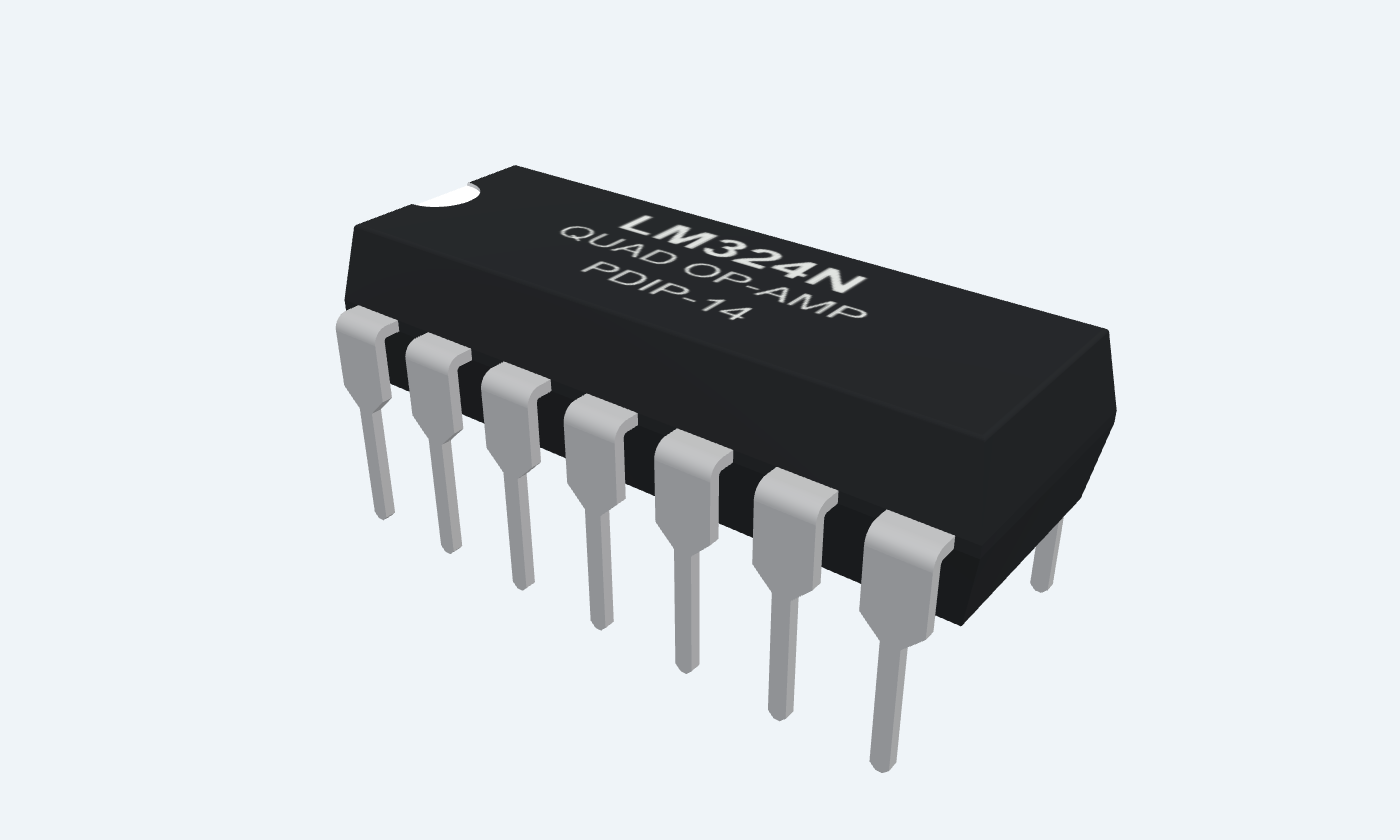
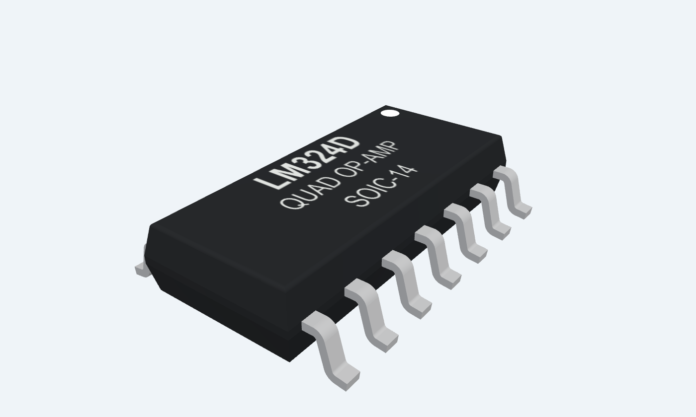

14Physical pins
LM324NPDIP-14
Manufacturer-referencedTexas Instruments
Pin diagram
Select a pin to explore its connection
Highlight
LM324NPDIP-14Top view
LM324DSOIC-14Top view
Click a lead or use the arrow keys. Top view
PIN 1 · Analog outputs
Analog outputOUTA
Function
Amplifier A output.
How to connect
Connect the 30 kΩ feedback resistor and high-impedance output meter.
Electrical note
Output is not rail-to-rail; load and temperature affect the swing.
PIN 2 · Amplifier inputs
Inverting inputINA−
Function
Negative feedback input of amplifier A.
How to connect
Connect the 30 kΩ / 10 kΩ feedback junction.
PIN 3 · Amplifier inputs
Non-inverting inputINA+
Function
Positive signal input of amplifier A.
How to connect
Connect to VIN in the example.
Electrical note
Keep the input within the recommended common-mode range.
PIN 4 · Supply
Positive supplyVCC+
Function
Positive supply shared by all four amplifiers.
How to connect
Apply +5 V; bypass locally to pin 11 with 100 nF.
PIN 5 · Amplifier inputs
Non-inverting inputINB+
Function
Positive signal input of amplifier B.
How to connect
Connect to VIN in the example.
Electrical note
Keep the input within the recommended common-mode range.
PIN 6 · Amplifier inputs
Inverting inputINB−
Function
Negative feedback input of amplifier B.
How to connect
Connect directly to OUTB for a unity-gain follower.
PIN 7 · Analog outputs
Analog outputOUTB
Function
Amplifier B output.
How to connect
Join to INB−; leave the follower output otherwise unloaded.
Electrical note
Output is not rail-to-rail; load and temperature affect the swing.
PIN 8 · Analog outputs
Analog outputOUTC
Function
Amplifier C output.
How to connect
Join to INC−; leave the follower output otherwise unloaded.
Electrical note
Output is not rail-to-rail; load and temperature affect the swing.
PIN 9 · Amplifier inputs
Inverting inputINC−
Function
Negative feedback input of amplifier C.
How to connect
Connect directly to OUTC for a unity-gain follower.
PIN 10 · Amplifier inputs
Non-inverting inputINC+
Function
Positive signal input of amplifier C.
How to connect
Connect to VIN in the example.
Electrical note
Keep the input within the recommended common-mode range.
PIN 11 · Supply
Negative supply / returnVCC−
Function
Negative supply shared by all four amplifiers.
How to connect
Connect to GND for the illustrated single-supply circuit.
Electrical note
With split supplies this is the negative rail, not the midpoint.
PIN 12 · Amplifier inputs
Non-inverting inputIND+
Function
Positive signal input of amplifier D.
How to connect
Connect to VIN in the example.
Electrical note
Keep the input within the recommended common-mode range.
PIN 13 · Amplifier inputs
Inverting inputIND−
Function
Negative feedback input of amplifier D.
How to connect
Connect directly to OUTD for a unity-gain follower.
PIN 14 · Analog outputs
Analog outputOUTD
Function
Amplifier D output.
How to connect
Join to IND−; leave the follower output otherwise unloaded.
Electrical note
Output is not rail-to-rail; load and temperature affect the swing.
Key specifications
Use the four amplifiers independently while keeping every input and feedback path defined.
Recommended supply3–30 V · classic LM324
Independent amplifiers4 Shared supply pins
Ambient range0–70 °C
Typical unity-gain bandwidth1.2 MHz · specified test conditions
Package details
LM324N · PDIP-14
| Property | Details |
|---|---|
| Manufacturer | Texas Instruments |
| Part number | LM324N |
| Package | PDIP-14 |
| Connections | 14 pins |
| Mounting | Through-hole |
| Lead pitch | 2.54 mm |
| Package code | dip |
| Thermal reference | Board and package dependent; see manufacturer data |
Operating conditions
Classic LM324N / LM324D
Manufacturer specifications 5 parameters
Scroll sideways to see all columns.
| Parameter | Value | Conditions / notes |
|---|---|---|
| Supply span | 3–30 V | VCC+ minus VCC− |
| Ambient temperature | 0 to +70°C | LM324 grade |
| Input common-mode range | 0 to VCC − 2 V | Full temperature; single-supply reference |
| Input range at 25°C | 0 to VCC − 1.5 V | Specified common-mode range |
| Unity-gain operation | Stable follower configuration | Use sensible load capacitance and layout |
No specifications match. Try a parameter name or a unit.
Specifications here refer to the classic LM324, not the newer B version.
Electrical characteristics
5 V unless stated
Manufacturer specifications 7 parameters
Scroll sideways to see all columns.
| Parameter | Value | Conditions / notes |
|---|---|---|
| Input offset voltage | 3 mV typical; 7 mV maximum | 25°C; VCC = 5–30 V |
| Offset over temperature | 9 mV maximum | 0–70°C |
| Input bias current | 20 nA typical; 250 nA maximum | Magnitude at 25°C |
| Open-loop voltage gain | 100 V/mV typical; 25 minimum | 15 V supply; VO = 1–11 V; RL ≥ 2 kΩ; 25°C |
| Total supply current | 0.7 mA typical; 1.2 mA maximum | Four amplifiers; 5 V; unloaded; VO = 2.5 V |
| Output LOW | 5 mV typical; 20 mV maximum | Specified RL ≤ 10 kΩ test |
| Output HIGH | Approximately VCC − 1.5 V | Typical at 25°C; RL = 2 kΩ |
No specifications match. Try a parameter name or a unit.
Output swing depends on the load and operating point; it is not a rail-to-rail specification.
Dynamic characteristics
Specified ±15 V tests · 25°C
Manufacturer specifications 5 parameters
Scroll sideways to see all columns.
| Parameter | Value | Conditions / notes |
|---|---|---|
| Unity-gain bandwidth | 1.2 MHz typical | RL = 1 MΩ; CL = 20 pF |
| Unity-gain slew rate | 0.5 V/µs typical | RL = 1 MΩ; CL = 30 pF; VI = ±10 V |
| Input noise voltage | 35 nV/√Hz typical | RS = 100 Ω; VI = 0 V; f = 1 kHz |
| Closed-loop bandwidth | Decreases as gain increases | First-order estimate: bandwidth ≈ GBW / gain |
| Large-signal sine wave | Slew rate can dominate | Required SR = 2π × frequency × peak amplitude |
No specifications match. Try a parameter name or a unit.
These typical tests do not guarantee the same bandwidth at every supply, gain or load.
Non-inverting amplifier
Gain four at a 5 V supply
Manufacturer specifications 7 parameters
Scroll sideways to see all columns.
| Parameter | Value | Conditions / notes |
|---|---|---|
| Input voltage | 0.40 V | To IN A+ pin 3 |
| Feedback resistor | 30 kΩ | OUT A pin 1 to IN A− pin 2 |
| Ground resistor | 10 kΩ | IN A− pin 2 to GND |
| Ideal gain | 4 V/V | 1 + 30 / 10 |
| Ideal output | 1.60 V | 0.40 × 4 |
| Other channels | Unity-gain followers at VIN | B: 7→6; C: 8→9; D: 14→13 |
| Bypass capacitor | 100 nF | Between pins 4 and 11 |
No specifications match. Try a parameter name or a unit.
Follower inputs: B pin 5, C pin 10 and D pin 12. Outputs otherwise unloaded.
Package and connection reference
LM324N · PDIP-14
Manufacturer specifications 6 parameters
Scroll sideways to see all columns.
| Parameter | Value | Conditions / notes |
|---|---|---|
| Lead pitch | 2.54 mm | Through-hole; top view |
| Channel A | IN+ 3; IN− 2; OUT 1 | First amplifier |
| Channel B | IN+ 5; IN− 6; OUT 7 | Second amplifier |
| Channel C | IN+ 10; IN− 9; OUT 8 | Third amplifier |
| Channel D | IN+ 12; IN− 13; OUT 14 | Fourth amplifier |
| Shared rails | VCC+ 4; VCC− 11 | Do not copy LM358 power-pin numbers |
No specifications match. Try a parameter name or a unit.
Verify the exact package and pin-one mark before board manufacture.
Connections by function
Select a pin for its function, connection guidance and electrical notes.
Analog outputs4 pins
Amplifier inputs8 pins
Supply2 pins
Analog outputs4 pins
Amplifier inputs8 pins
Supply2 pins
LM324 at a glance
Follow the labeled connections and functional stages
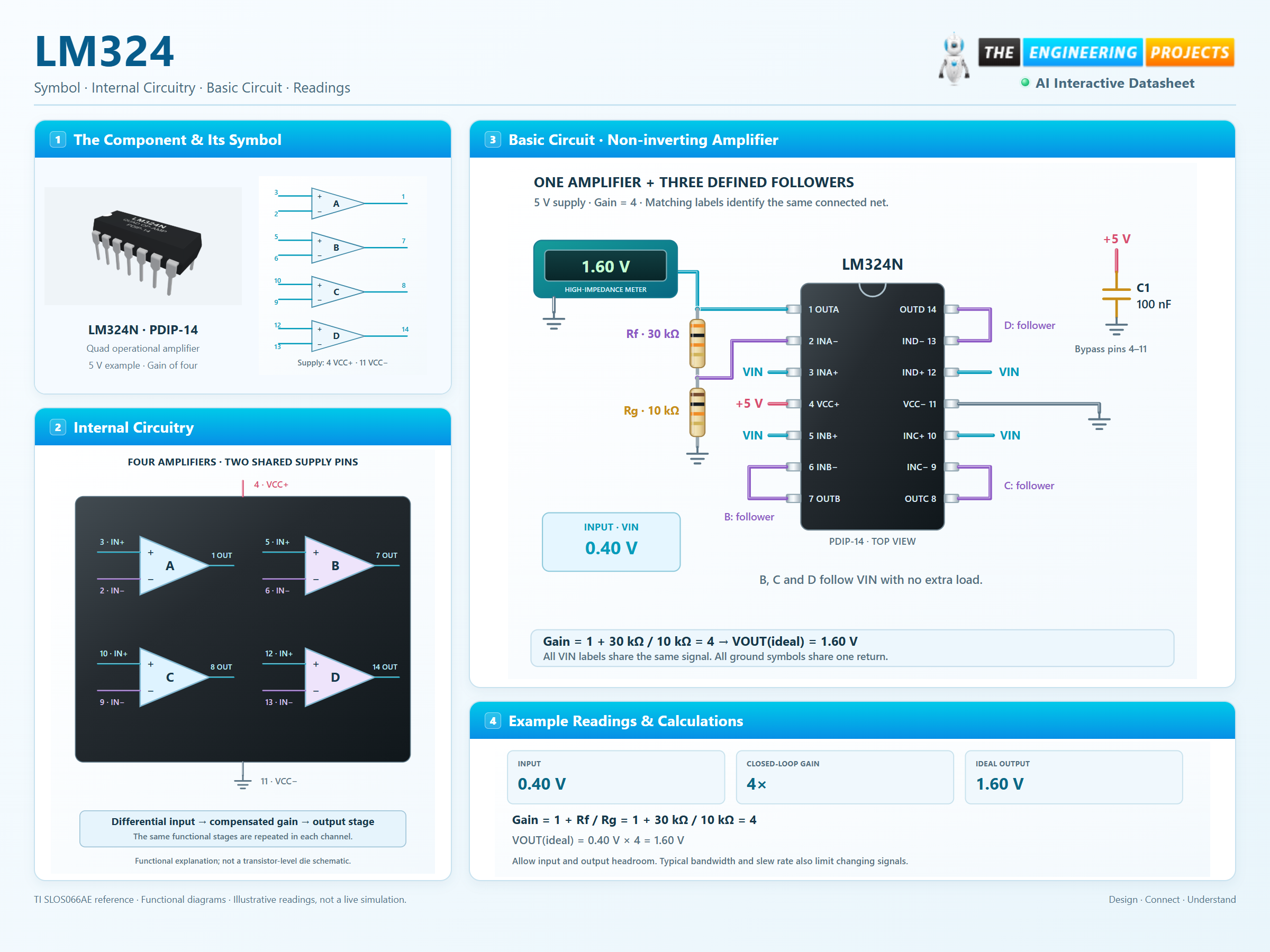
How it works
3 stages · Explore one step at a time
Sense the input difference
Each differential input stage responds to IN+ minus IN−. Open-loop gain is very high, so practical linear circuits use negative feedback.
Set gain with two resistors
For the non-inverting connection, gain is 1 + Rf/Rg. With 30 kΩ and 10 kΩ the nominal gain is four.
Respect the analog limits
The output cannot reach the positive supply rail. Input range, output load, slew rate and bandwidth all limit how closely the real output follows the ideal result.
Step 1 of 3
LM324 in a circuit
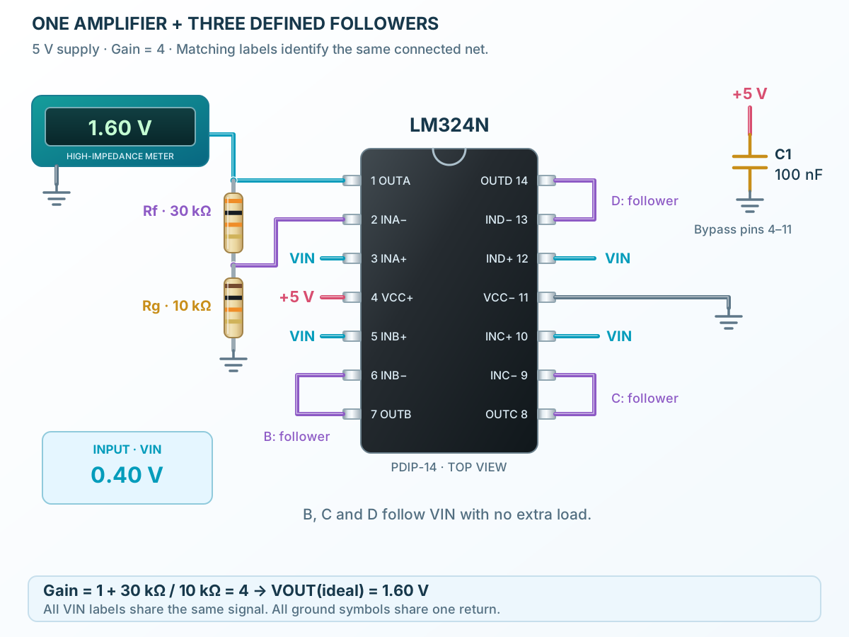
A physical 14-pin IC with one amplifier and three defined followers.
Connect it, step by step
Follow the component values and pin connections
Set the gain
Rf = 30 kΩ and Rg = 10 kΩ set a nominal gain of four.
Connect all four channels
Channel A amplifies VIN. B, C and D follow VIN, with their outputs connected to their own negative inputs.
Check headroom
0.40 V ideally becomes 1.60 V. Increase VIN in the explorer to see the output approach its estimated upper limit.
Try the amplifier
Change the input and feedback. See the gain and output respond.
Closed-loop gain—
Ideal output—
Estimated output—
Enable JavaScript to explore the amplifier.
Estimated outputIdeal gainInput outside recommended range
Gain = 1 + Rf / Rg · VOUT(ideal) = VIN × Gain
Illustrative DC model at 5 V and a light load: output limits are estimated at 0.02 V and 3.50 V. Real swing depends on load, temperature and part variation. Offset, bandwidth, slew rate and noise are omitted; this is a teaching explorer rather than a transistor-level simulation.
Inside LM324
Four independent amplifiers share the same two power rails.
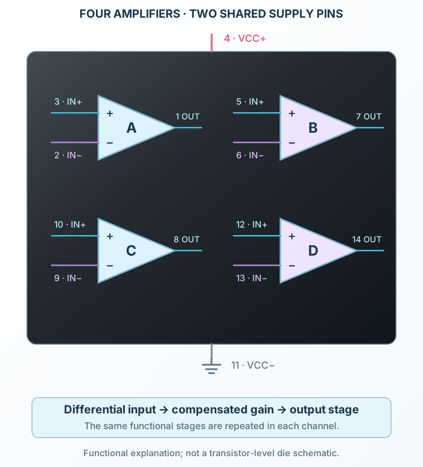
Explore the circuit
Select a stage to see its role and connections
Four differential inputs
Each channel has a separate input pair and output.
Compensated gain
Internal compensation supports unity-gain operation. Frequency response still limits fast signals.
Shared rails
Pin 4 supplies the positive rail and pin 11 the negative rail or ground.
Selected packagePDIP-14LM324N
Physical connections14 pinsPackage-specific numbering
Reference collection6 tables30 parameters & pin functions
Pin reference
Signal names, electrical functions and connection guidance
Physical pin numbers14 pins
Scroll within the table to see all columns and rows.
| Pin | Signal | Type | Function & connection |
|---|---|---|---|
| OUTA | Analog output | Amplifier A output.Connection guidanceConnect the 30 kΩ feedback resistor and high-impedance output meter. Output is not rail-to-rail; load and temperature affect the swing. | |
| INA− | Inverting input | Negative feedback input of amplifier A.Connection guidanceConnect the 30 kΩ / 10 kΩ feedback junction. | |
| INA+ | Non-inverting input | Positive signal input of amplifier A.Connection guidanceConnect to VIN in the example. Keep the input within the recommended common-mode range. | |
| VCC+ | Positive supply | Positive supply shared by all four amplifiers.Connection guidanceApply +5 V; bypass locally to pin 11 with 100 nF. | |
| INB+ | Non-inverting input | Positive signal input of amplifier B.Connection guidanceConnect to VIN in the example. Keep the input within the recommended common-mode range. | |
| INB− | Inverting input | Negative feedback input of amplifier B.Connection guidanceConnect directly to OUTB for a unity-gain follower. | |
| OUTB | Analog output | Amplifier B output.Connection guidanceJoin to INB−; leave the follower output otherwise unloaded. Output is not rail-to-rail; load and temperature affect the swing. | |
| OUTC | Analog output | Amplifier C output.Connection guidanceJoin to INC−; leave the follower output otherwise unloaded. Output is not rail-to-rail; load and temperature affect the swing. | |
| INC− | Inverting input | Negative feedback input of amplifier C.Connection guidanceConnect directly to OUTC for a unity-gain follower. | |
| INC+ | Non-inverting input | Positive signal input of amplifier C.Connection guidanceConnect to VIN in the example. Keep the input within the recommended common-mode range. | |
| VCC− | Negative supply / return | Negative supply shared by all four amplifiers.Connection guidanceConnect to GND for the illustrated single-supply circuit. With split supplies this is the negative rail, not the midpoint. | |
| IND+ | Non-inverting input | Positive signal input of amplifier D.Connection guidanceConnect to VIN in the example. Keep the input within the recommended common-mode range. | |
| IND− | Inverting input | Negative feedback input of amplifier D.Connection guidanceConnect directly to OUTD for a unity-gain follower. | |
| OUTD | Analog output | Amplifier D output.Connection guidanceJoin to IND−; leave the follower output otherwise unloaded. Output is not rail-to-rail; load and temperature affect the swing. |
No pins match these filters. Try another signal name or reset the filters.
Operating conditions
Classic LM324N / LM324D
Manufacturer-referenced values5 parameters
Scroll within the table to see all columns and rows.
| Parameter | Value | Conditions / notes |
|---|---|---|
| Supply span | 3–30 V | VCC+ minus VCC− |
| Ambient temperature | 0 to +70°C | LM324 grade |
| Input common-mode range | 0 to VCC − 2 V | Full temperature; single-supply reference |
| Input range at 25°C | 0 to VCC − 1.5 V | Specified common-mode range |
| Unity-gain operation | Stable follower configuration | Use sensible load capacitance and layout |
No specifications match. Try a parameter name or a unit.
Specifications here refer to the classic LM324, not the newer B version.
Electrical characteristics
5 V unless stated
Manufacturer-referenced values7 parameters
Scroll within the table to see all columns and rows.
| Parameter | Value | Conditions / notes |
|---|---|---|
| Input offset voltage | 3 mV typical; 7 mV maximum | 25°C; VCC = 5–30 V |
| Offset over temperature | 9 mV maximum | 0–70°C |
| Input bias current | 20 nA typical; 250 nA maximum | Magnitude at 25°C |
| Open-loop voltage gain | 100 V/mV typical; 25 minimum | 15 V supply; VO = 1–11 V; RL ≥ 2 kΩ; 25°C |
| Total supply current | 0.7 mA typical; 1.2 mA maximum | Four amplifiers; 5 V; unloaded; VO = 2.5 V |
| Output LOW | 5 mV typical; 20 mV maximum | Specified RL ≤ 10 kΩ test |
| Output HIGH | Approximately VCC − 1.5 V | Typical at 25°C; RL = 2 kΩ |
No specifications match. Try a parameter name or a unit.
Output swing depends on the load and operating point; it is not a rail-to-rail specification.
Dynamic characteristics
Specified ±15 V tests · 25°C
Manufacturer-referenced values5 parameters
Scroll within the table to see all columns and rows.
| Parameter | Value | Conditions / notes |
|---|---|---|
| Unity-gain bandwidth | 1.2 MHz typical | RL = 1 MΩ; CL = 20 pF |
| Unity-gain slew rate | 0.5 V/µs typical | RL = 1 MΩ; CL = 30 pF; VI = ±10 V |
| Input noise voltage | 35 nV/√Hz typical | RS = 100 Ω; VI = 0 V; f = 1 kHz |
| Closed-loop bandwidth | Decreases as gain increases | First-order estimate: bandwidth ≈ GBW / gain |
| Large-signal sine wave | Slew rate can dominate | Required SR = 2π × frequency × peak amplitude |
No specifications match. Try a parameter name or a unit.
These typical tests do not guarantee the same bandwidth at every supply, gain or load.
Non-inverting amplifier
Gain four at a 5 V supply
Manufacturer-referenced values7 parameters
Scroll within the table to see all columns and rows.
| Parameter | Value | Conditions / notes |
|---|---|---|
| Input voltage | 0.40 V | To IN A+ pin 3 |
| Feedback resistor | 30 kΩ | OUT A pin 1 to IN A− pin 2 |
| Ground resistor | 10 kΩ | IN A− pin 2 to GND |
| Ideal gain | 4 V/V | 1 + 30 / 10 |
| Ideal output | 1.60 V | 0.40 × 4 |
| Other channels | Unity-gain followers at VIN | B: 7→6; C: 8→9; D: 14→13 |
| Bypass capacitor | 100 nF | Between pins 4 and 11 |
No specifications match. Try a parameter name or a unit.
Follower inputs: B pin 5, C pin 10 and D pin 12. Outputs otherwise unloaded.
Package and connection reference
LM324N · PDIP-14
Manufacturer-referenced values6 parameters
Scroll within the table to see all columns and rows.
| Parameter | Value | Conditions / notes |
|---|---|---|
| Lead pitch | 2.54 mm | Through-hole; top view |
| Channel A | IN+ 3; IN− 2; OUT 1 | First amplifier |
| Channel B | IN+ 5; IN− 6; OUT 7 | Second amplifier |
| Channel C | IN+ 10; IN− 9; OUT 8 | Third amplifier |
| Channel D | IN+ 12; IN− 13; OUT 14 | Fourth amplifier |
| Shared rails | VCC+ 4; VCC− 11 | Do not copy LM358 power-pin numbers |
No specifications match. Try a parameter name or a unit.
Verify the exact package and pin-one mark before board manufacture.
No matching rowsTry a pin name, parameter, unit or test condition, or reset the filters.
Sensor signal conditioning
Amplify low-frequency sensor signals into an ADC range while respecting input and output limits.
Manufacturer application guideActive filters
Combine resistors, capacitors and feedback to build low-frequency filters. Check bandwidth and loading.
Manufacturer application guideMultiple buffers
Use independent followers to isolate several signal nodes from later stages. Keep unused channels in stable closed-loop configurations.
Manufacturer application guideTake it into ProTech
Find LM324 in the Components Library to place its schematic symbol and connect its pins.
Reference page · circuit simulation model not yet availableOpen ProTech