Real View
Turn a voltage threshold into a clear digital decision.
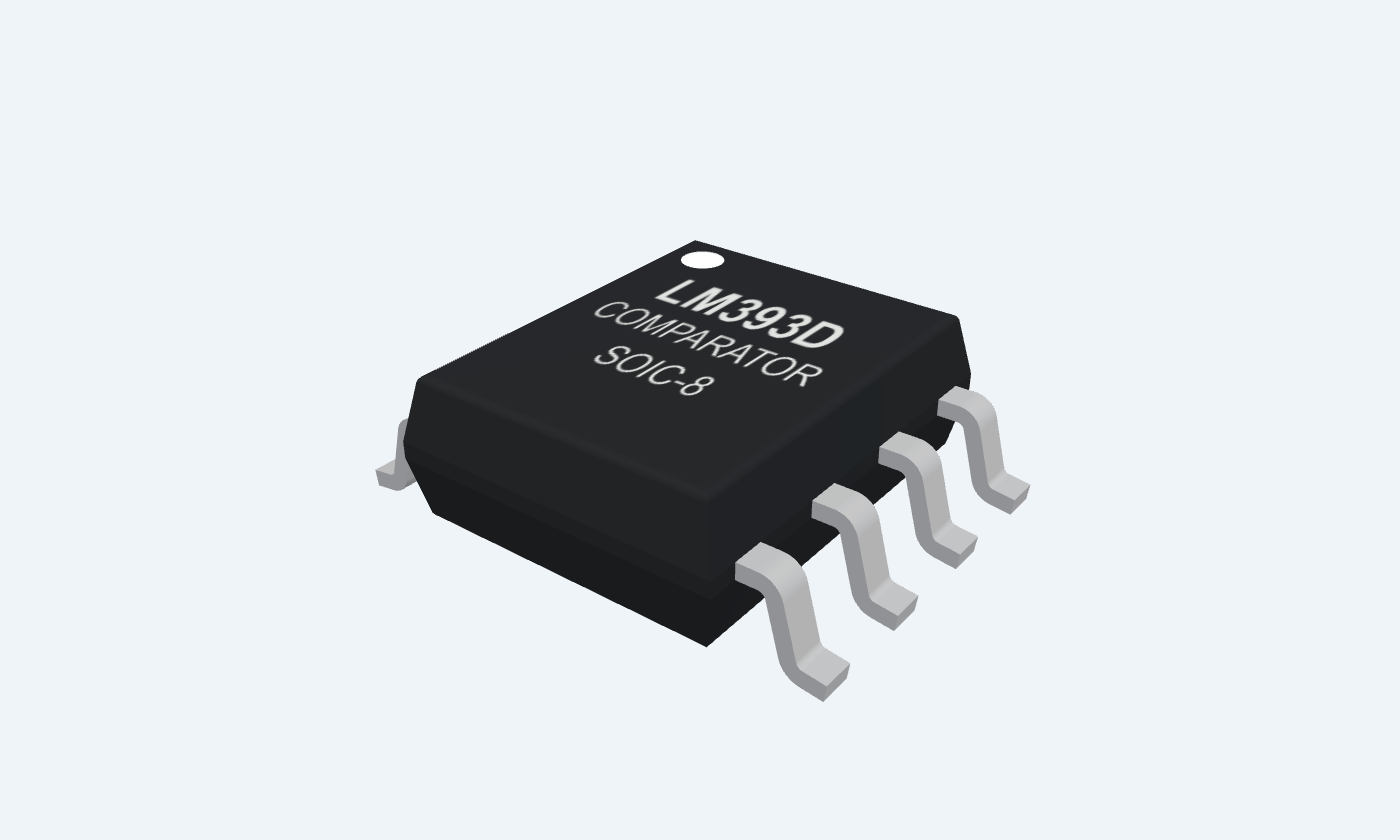
LM393 contains two independent voltage comparators in an eight-pin IC. Each compares its positive and negative inputs and controls an open-collector output. When IN+ is below IN−, the output transistor conducts and pulls the output LOW. When IN+ rises above IN−, it releases the output and an external pull-up resistor establishes HIGH. This reference covers the classic LM393P and LM393D, with a 5 V threshold detector and a 2 V reference.
Select a pin to explore its connection
Click a lead or use the arrow keys. Top view
Channel A sinks current when IN1− is above IN1+.
Add a 10 kΩ pull-up to +5 V; read this node with a high-impedance input.
The IC does not actively drive HIGH.
Channel A reference input in the illustrated circuit.
Connect the 2.00 V divider node.
Keep both example inputs within 0–3 V at a 5 V supply.
Channel A measured signal.
Connect VIN and a common ground.
Ground reference for both comparators.
Connect the supply return and bypass capacitor.
Channel B positive input.
Tie to GND when unused in this example.
Channel B negative input.
Connect to the same 2 V reference to give the unused channel a defined state.
Channel B current-sinking output.
Leave unconnected in the single-channel example.
Use a separate pull-up when using channel B.
Shared positive supply for both comparators.
Apply +5 V; place 100 nF between pins 8 and 4.
Classic LM393 recommended supply: 2–30 V.
An open-collector output needs a pull-up resistor. It sinks current instead of sourcing a HIGH level.
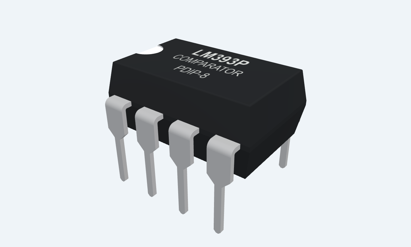
LM393P · PDIP-8
| Property | Details |
|---|---|
| Manufacturer | Texas Instruments |
| Part number | LM393P |
| Package | PDIP-8 |
| Connections | 8 pins |
| Mounting | Through-hole |
| Lead pitch | 2.54 mm |
| Package code | dip |
| Thermal reference | Board and package dependent; see manufacturer data |
Classic LM393 · not the B revision
Scroll sideways to see all columns.
| Parameter | Value | Conditions / notes |
|---|---|---|
| Supply | 2–30 V | Single supply; example uses 5 V |
| Ambient temperature | 0 to +70°C | LM393 / LM393A grade |
| Input voltage range | 0 to VCC − 2 V | Recommended full-temperature range |
| Example input range | 0–3 V | At VCC = 5 V |
| Output HIGH | External pull-up required | Output transistor is off |
No specifications match. Try a parameter name or a unit.
TI SLCS005AH recommended conditions for the classic device.
5 V supply unless stated
Scroll sideways to see all columns.
| Parameter | Value | Conditions / notes |
|---|---|---|
| Input offset voltage | 2 mV typical; 5 mV maximum | 25°C; VCC = 5–30 V |
| Offset over temperature | 9 mV maximum | 0–70°C |
| Input bias current | 25 nA typical; 250 nA maximum | Magnitude at 25°C |
| Output LOW voltage | 0.13 V typical; 0.40 V maximum | 4 mA sink; VID = −1 V; 25°C |
| Output LOW over temperature | 0.70 V maximum | Same 4 mA test; full range |
| Total supply current | 0.45 mA typical; 1 mA maximum | 5 V; unloaded; 25°C |
| Response time | 1.3 µs typical | 100 mV step; 5 mV overdrive; 5.1 kΩ pull-up; 15 pF |
No specifications match. Try a parameter name or a unit.
Response time and typical LOW voltage are not guaranteed operating limits.
Voltage difference and pull-up
Scroll sideways to see all columns.
| Parameter | Value | Conditions / notes |
|---|---|---|
| IN+ < IN− | Output transistor ON | LOW; current flows through the pull-up |
| IN+ > IN− | Output transistor OFF | HIGH only with a pull-up or another defined load |
| Inputs nearly equal | Offset and noise matter | Output state is not guaranteed at exact equality |
| No pull-up; transistor OFF | Floating output | Do not call this HIGH |
| Noisy threshold | May switch repeatedly | Use calculated hysteresis for a stable transition |
No specifications match. Try a parameter name or a unit.
This example has no positive-feedback hysteresis.
Nominal 5 V example
Scroll sideways to see all columns.
| Parameter | Value | Conditions / notes |
|---|---|---|
| Upper reference resistor | 30 kΩ | From +5 V to VREF |
| Lower reference resistor | 20 kΩ | From VREF to ground |
| Reference voltage | 2.00 V | 5 × 20 / (30 + 20) |
| Output pull-up | 10 kΩ | From +5 V to OUT1 |
| Supply bypass | 100 nF | Close to pins 8 and 4 |
| Unused comparator | IN2+ to GND; IN2− to VREF | OUT2 unconnected |
No specifications match. Try a parameter name or a unit.
Divider tolerance, input bias and supply error affect the threshold.
LM393P · PDIP-8
Scroll sideways to see all columns.
| Parameter | Value | Conditions / notes |
|---|---|---|
| Lead pitch | 2.54 mm | Through-hole; top view |
| Supply absolute maximum | 36 V | Stress rating; recommended maximum is 30 V |
| Output voltage absolute maximum | −0.3 to +36 V | Observe the load and current limits |
| Output current absolute maximum | 20 mA | Not a recommended design current |
| Junction temperature limit | 150°C | Absolute maximum |
| Storage temperature | −65 to +150°C | Unpowered storage |
No specifications match. Try a parameter name or a unit.
Use the manufacturer thermal data for the actual board and package.
Select a pin for its function, connection guidance and electrical notes.
Follow the labeled connections and functional stages
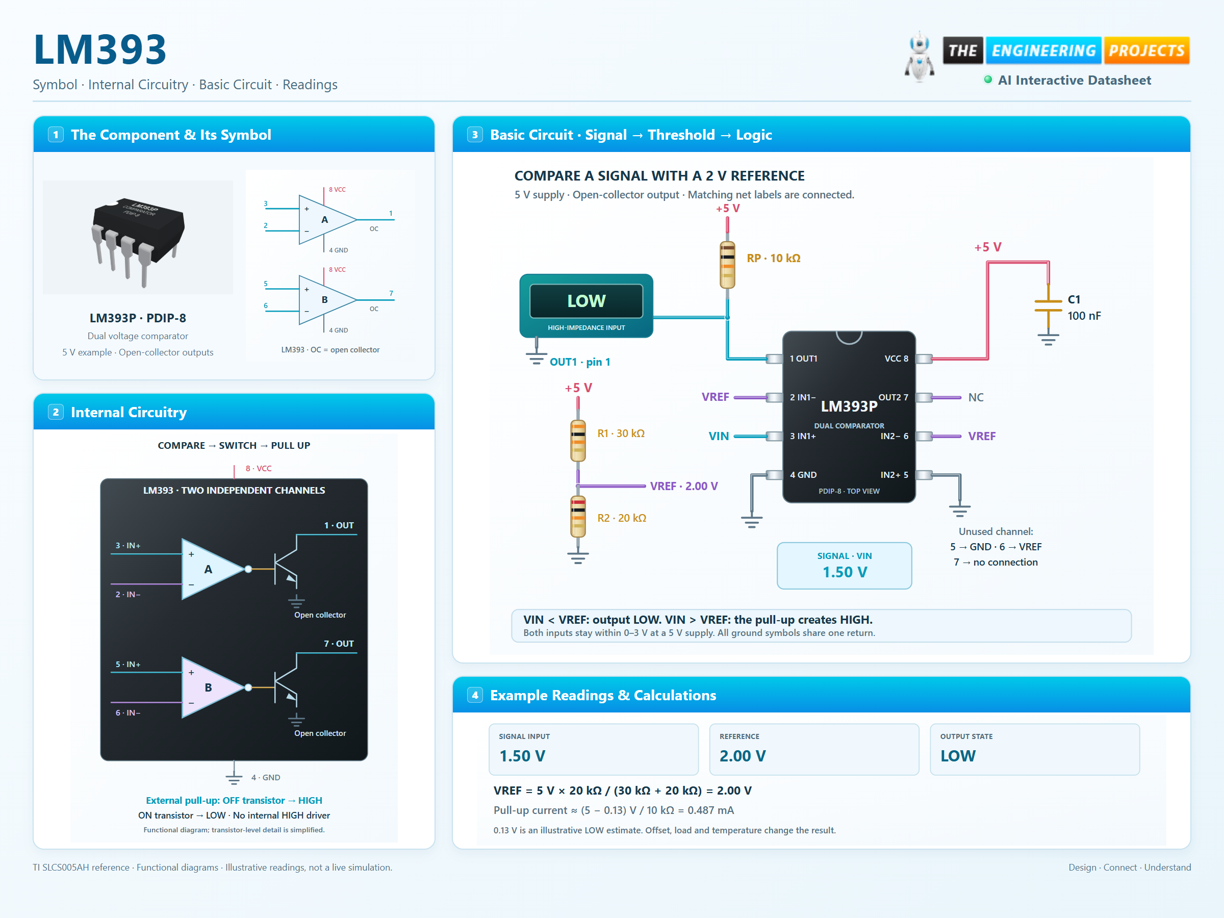
3 stages · Explore one step at a time
The differential input stage responds to IN+ minus IN−. No analog-to-digital converter or firmware is needed.
A negative input difference turns the output transistor on. A positive difference turns it off. The external pull-up supplies the HIGH level.
Keep inputs in their common-mode range. Add positive-feedback hysteresis when a slowly changing or noisy signal would chatter around the threshold.
Adjust VIN and the reference. Remove the pull-up to see why it matters.
Enable JavaScript to explore the comparator.
Violet: offset-sensitive transition · Amber: input outside the recommended range.
DC teaching model for channel A. The ±9 mV band uses the maximum input-offset magnitude over 0–70°C; it is uncertainty, not hysteresis. LOW uses a 0.13 V illustrative estimate. Propagation delay, input bias, leakage and noise are omitted.
A physical IC, a resistor reference and a clearly defined output.
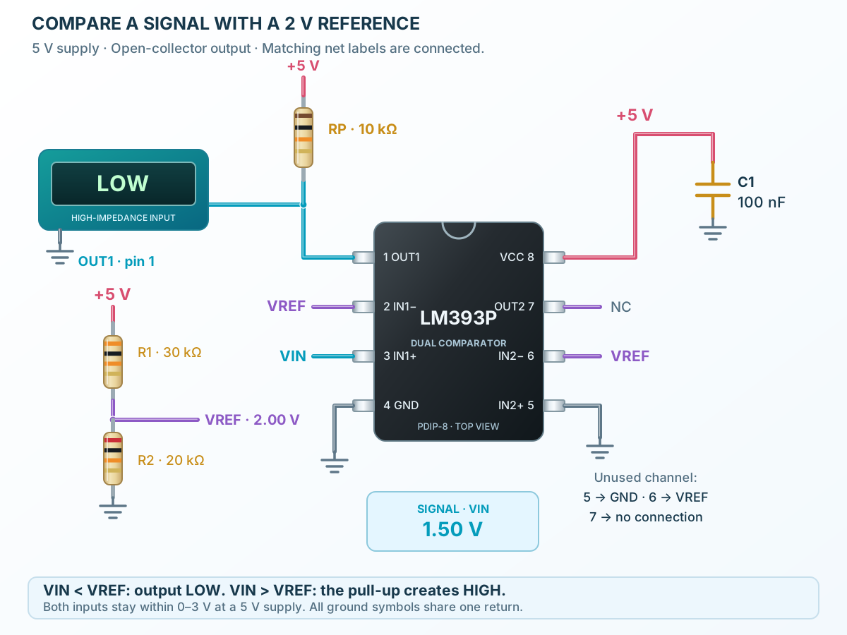
Follow the component values and pin connections
30 kΩ above and 20 kΩ below produce a nominal 2 V reference from 5 V.
Connect the measured voltage to IN1+ and VREF to IN1−. VIN below 2 V makes OUT1 LOW.
Connect 10 kΩ from OUT1 to 5 V. Without it, the released output is floating rather than HIGH.
Two differential channels with independent open-collector outputs.
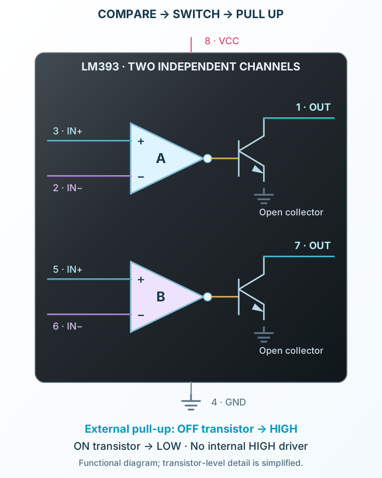
Select a stage to see its role and connections
Compare the two input voltages while respecting their valid range.
The collector is exposed at OUT. A LOW state sinks current; an off transistor releases the node.
Both channels use VCC pin 8 and GND pin 4, but each has its own inputs and output.
Signal names, electrical functions and connection guidance
Scroll within the table to see all columns and rows.
| Pin | Signal | Type | Function & connection |
|---|---|---|---|
| OUT1 | Open-collector output | Channel A sinks current when IN1− is above IN1+.Connection guidanceAdd a 10 kΩ pull-up to +5 V; read this node with a high-impedance input. The IC does not actively drive HIGH. | |
| IN1− | Inverting input | Channel A reference input in the illustrated circuit.Connection guidanceConnect the 2.00 V divider node. Keep both example inputs within 0–3 V at a 5 V supply. | |
| IN1+ | Non-inverting input | Channel A measured signal.Connection guidanceConnect VIN and a common ground. | |
| GND | Supply return | Ground reference for both comparators.Connection guidanceConnect the supply return and bypass capacitor. | |
| IN2+ | Non-inverting input | Channel B positive input.Connection guidanceTie to GND when unused in this example. | |
| IN2− | Inverting input | Channel B negative input.Connection guidanceConnect to the same 2 V reference to give the unused channel a defined state. | |
| OUT2 | Open-collector output | Channel B current-sinking output.Connection guidanceLeave unconnected in the single-channel example. Use a separate pull-up when using channel B. | |
| VCC | Positive supply | Shared positive supply for both comparators.Connection guidanceApply +5 V; place 100 nF between pins 8 and 4. Classic LM393 recommended supply: 2–30 V. |
No pins match these filters. Try another signal name or reset the filters.
Classic LM393 · not the B revision
Scroll within the table to see all columns and rows.
| Parameter | Value | Conditions / notes |
|---|---|---|
| Supply | 2–30 V | Single supply; example uses 5 V |
| Ambient temperature | 0 to +70°C | LM393 / LM393A grade |
| Input voltage range | 0 to VCC − 2 V | Recommended full-temperature range |
| Example input range | 0–3 V | At VCC = 5 V |
| Output HIGH | External pull-up required | Output transistor is off |
No specifications match. Try a parameter name or a unit.
TI SLCS005AH recommended conditions for the classic device.
5 V supply unless stated
Scroll within the table to see all columns and rows.
| Parameter | Value | Conditions / notes |
|---|---|---|
| Input offset voltage | 2 mV typical; 5 mV maximum | 25°C; VCC = 5–30 V |
| Offset over temperature | 9 mV maximum | 0–70°C |
| Input bias current | 25 nA typical; 250 nA maximum | Magnitude at 25°C |
| Output LOW voltage | 0.13 V typical; 0.40 V maximum | 4 mA sink; VID = −1 V; 25°C |
| Output LOW over temperature | 0.70 V maximum | Same 4 mA test; full range |
| Total supply current | 0.45 mA typical; 1 mA maximum | 5 V; unloaded; 25°C |
| Response time | 1.3 µs typical | 100 mV step; 5 mV overdrive; 5.1 kΩ pull-up; 15 pF |
No specifications match. Try a parameter name or a unit.
Response time and typical LOW voltage are not guaranteed operating limits.
Voltage difference and pull-up
Scroll within the table to see all columns and rows.
| Parameter | Value | Conditions / notes |
|---|---|---|
| IN+ < IN− | Output transistor ON | LOW; current flows through the pull-up |
| IN+ > IN− | Output transistor OFF | HIGH only with a pull-up or another defined load |
| Inputs nearly equal | Offset and noise matter | Output state is not guaranteed at exact equality |
| No pull-up; transistor OFF | Floating output | Do not call this HIGH |
| Noisy threshold | May switch repeatedly | Use calculated hysteresis for a stable transition |
No specifications match. Try a parameter name or a unit.
This example has no positive-feedback hysteresis.
Nominal 5 V example
Scroll within the table to see all columns and rows.
| Parameter | Value | Conditions / notes |
|---|---|---|
| Upper reference resistor | 30 kΩ | From +5 V to VREF |
| Lower reference resistor | 20 kΩ | From VREF to ground |
| Reference voltage | 2.00 V | 5 × 20 / (30 + 20) |
| Output pull-up | 10 kΩ | From +5 V to OUT1 |
| Supply bypass | 100 nF | Close to pins 8 and 4 |
| Unused comparator | IN2+ to GND; IN2− to VREF | OUT2 unconnected |
No specifications match. Try a parameter name or a unit.
Divider tolerance, input bias and supply error affect the threshold.
LM393P · PDIP-8
Scroll within the table to see all columns and rows.
| Parameter | Value | Conditions / notes |
|---|---|---|
| Lead pitch | 2.54 mm | Through-hole; top view |
| Supply absolute maximum | 36 V | Stress rating; recommended maximum is 30 V |
| Output voltage absolute maximum | −0.3 to +36 V | Observe the load and current limits |
| Output current absolute maximum | 20 mA | Not a recommended design current |
| Junction temperature limit | 150°C | Absolute maximum |
| Storage temperature | −65 to +150°C | Unpowered storage |
No specifications match. Try a parameter name or a unit.
Use the manufacturer thermal data for the actual board and package.
No matching rowsTry a pin name, parameter, unit or test condition, or reset the filters.
Compare a sensor voltage with a reference and feed the result to logic. Choose a pull-up voltage compatible with that logic.
Manufacturer application guideUse both comparators for upper and lower limits. The output circuit determines how the two decisions combine.
Manufacturer application guideConvert a temperature, light or position voltage into an alarm state. Hysteresis prevents noisy repeated transitions.
Manufacturer application guideFind LM393 in the Components Library to place its schematic symbol and connect its pins.
Reference page · circuit simulation model not yet availableOpen ProTech