Real View
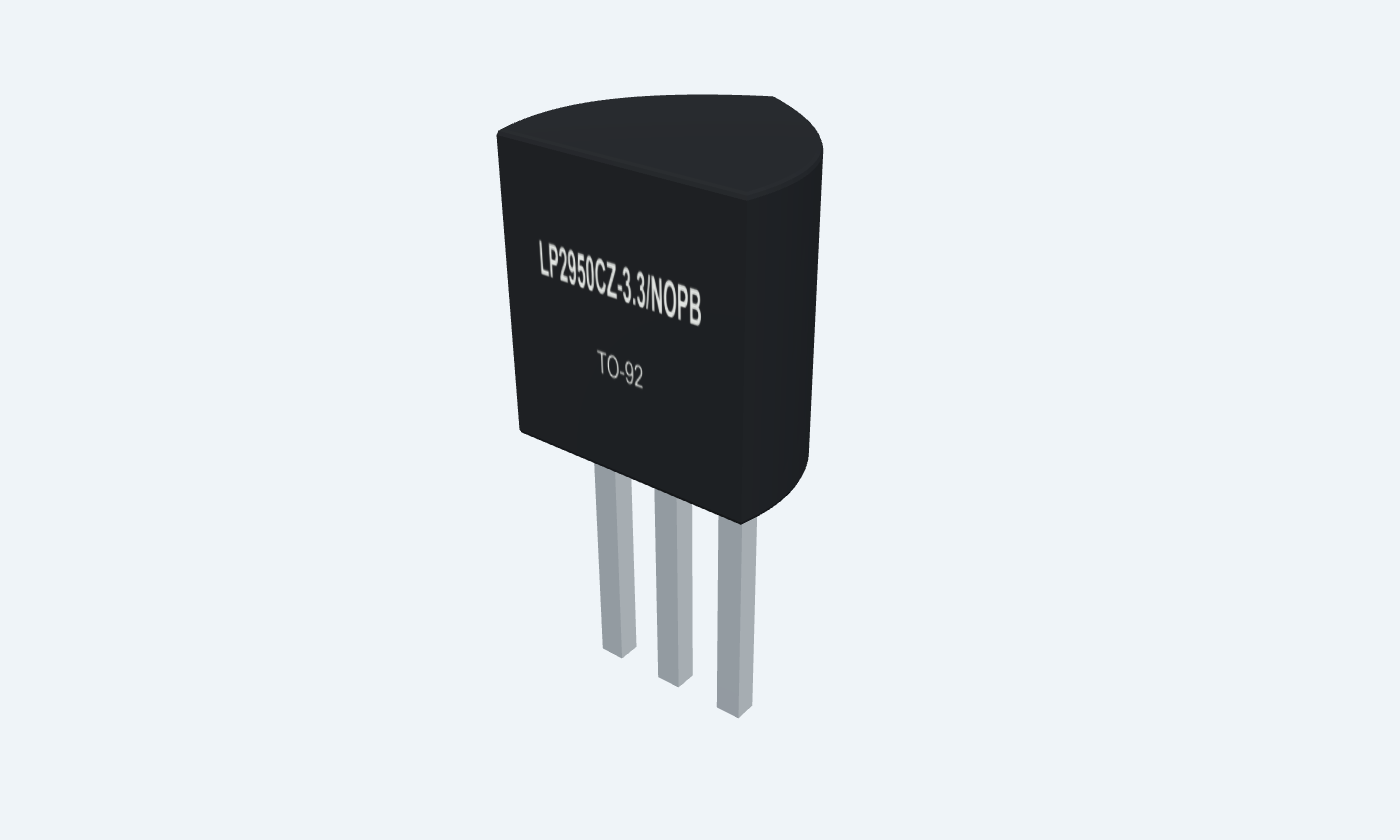
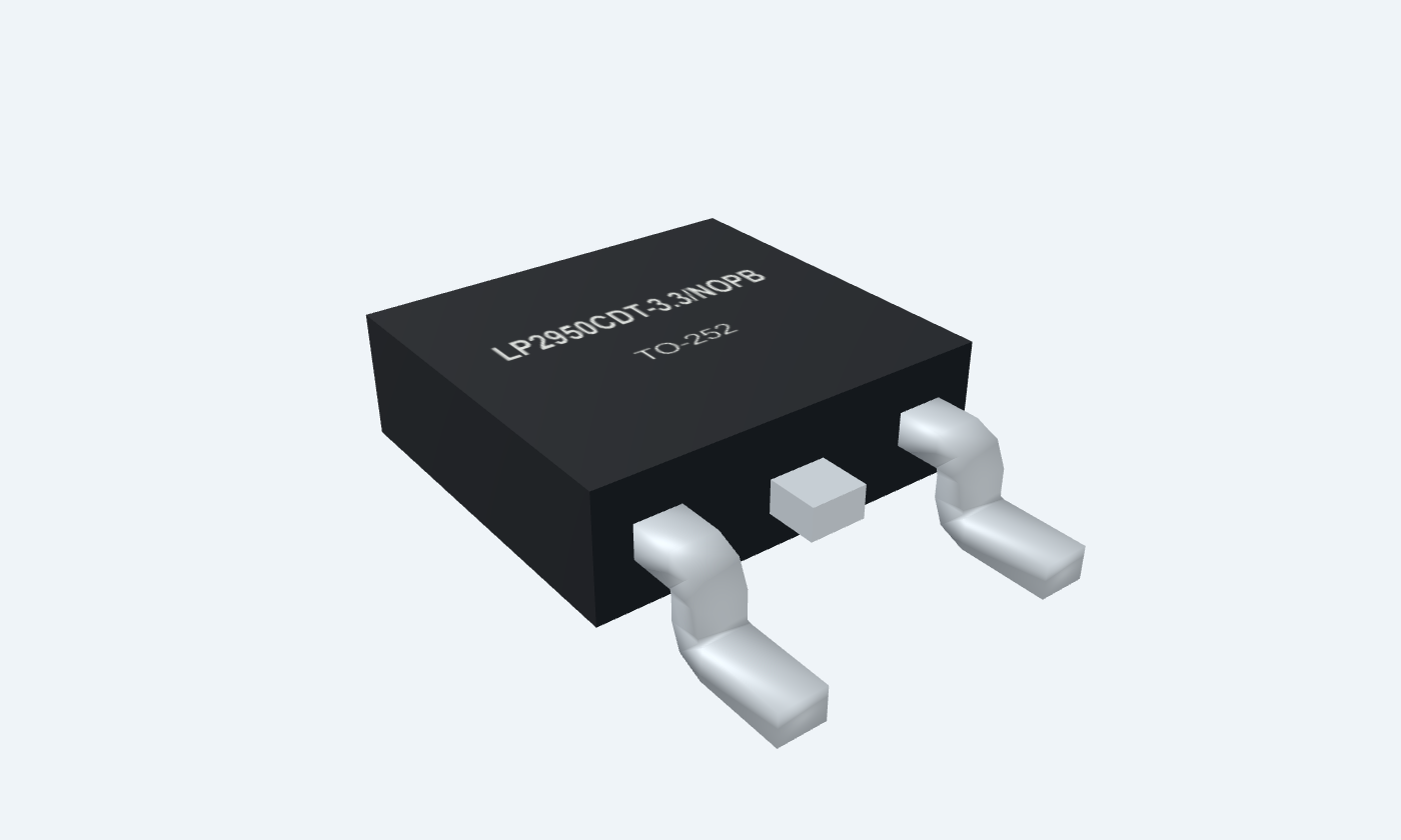
A quiet 3.3 V rail with very little standby current.
LP2950-3.3 is a three-terminal low-dropout regulator for a fixed 3.3 V rail, supplying up to 100 mA when input headroom and temperature permit. The low ground current at light load makes it useful for modest battery-powered analog and digital circuits. This page covers TI C-grade LP2950CZ-3.3/NOPB in TO-92 and LP2950CDT-3.3/NOPB in TO-252. Their OUT and IN pin numbers are reversed: TO-92 uses OUT1/GND2/IN3, while TO-252 uses IN1/GND2/OUT3 with a grounded tab. All package views follow that selection. A suitable output capacitor is essential for stability. The illustrated 5 V to 3.3 V supply uses local 1 µF input bypass, a 10 µF output capacitor with verified ESR, and a 330 Ω test load. The related LP2951 adds control functions; the three-pin LP2950 has no shutdown or error output.
Select a pin to explore its connection
Click a lead or use the arrow keys. Front view · flat face toward you · 1 OUT, 2 GND, 3 IN
Fixed 3.3 V output; an external stability capacitor is required.
Connect to the load and 10 µF output capacitor; return both to GND.
TO-92 pin 1; TO-252 pin 3. Use the selected package map.
Reference and bias-current return for the regulator.
Join input return, output capacitor and load grounds locally.
Pin 2 in both packages; TO-252 exposed tab is also GND.
Supply input for the protected series-pass stage.
Use +5 V in the example and local 1 µF bypass.
TO-92 pin 3; TO-252 pin 1. Maximum operating input 30 V; allow design margin.
An internal reference and feedback divider control a series-pass stage. Output capacitance, headroom and ground current remain part of the design.
LP2950CZ-3.3/NOPB · TO-92
| Property | Details |
|---|---|
| Manufacturer | Texas Instruments |
| Part number | LP2950CZ-3.3/NOPB |
| Package | TO-92 |
| Connections | 3 pins |
| Mounting | Through-hole |
| Lead pitch | 1.27 mm · straight leads |
| Package code | LP |
| Thermal reference | θJA 157.4°C/W under TI board conditions; actual mounting changes temperature rise |
C-grade fixed 3.3 V parts
Scroll sideways to see all columns.
| Parameter | Value | Conditions / notes |
|---|---|---|
| Through-hole order | LP2950CZ-3.3/NOPB | TO-92 LP; straight-lead bulk footprint |
| SMD order | LP2950CDT-3.3/NOPB | TO-252 NDP; formed outer leads and grounded tab |
| TO-92 physical pins | OUT1 · GND2 · IN3 | Flat face toward viewer, leads down |
| TO-252 physical pins | IN1 · GND2 · OUT3 | Front face, leads down; tab is GND |
| Accuracy grade | C: ±1% initial | AC-grade values are not substituted |
| Extra controls | No shutdown or error-output lead | These belong to the related LP2951 |
No specifications match. Try a parameter name or a unit.
Verify order suffix and lead form before fabrication.
Temperature and headroom remain essential
Scroll sideways to see all columns.
| Parameter | Value | Conditions / notes |
|---|---|---|
| Nominal output | 3.3 V | Fixed internally; no external divider |
| Recommended input range | 2.3–30 V family range | 3.3 V regulation additionally needs dropout headroom |
| Maximum input stress | 30 V | Do not design at the stress limit |
| Output-current class | 100 mA | Adequate voltage headroom and cooling required |
| Junction operating temperature | −40–125°C | Device junction, not ambient |
| Minimum external load | Not required for LP2950 regulation | Capacitor stability requirements still apply |
No specifications match. Try a parameter name or a unit.
A 2.3 V input cannot produce a regulated 3.3 V output.
3.3 V option; source conditions retained
Scroll sideways to see all columns.
| Parameter | Value | Conditions / notes |
|---|---|---|
| Output at 25°C | 3.267–3.333 V | Nominal 3.3 V |
| Output at −25 to 85°C | 3.251–3.350 V | Manufacturer specified range |
| Output over full temperature | 3.234–3.366 V | −40 to 125°C |
| Across 100 µA–100 mA load | 3.221–3.379 V | Full-temperature limit |
| Temperature coefficient | 50 ppm/°C typical; 150 max. | Output-voltage drift |
| Line regulation at 25°C | 0.04% typical; 0.2% max. | Input from VOUT(nom)+1 V to 30 V |
| Load regulation at 25°C | 0.1% typical; 0.2% max. | Load from 100 µA to 100 mA |
No specifications match. Try a parameter name or a unit.
AC-grade limits are tighter; this page deliberately uses the selected C-grade specification.
Load and temperature change both
Scroll sideways to see all columns.
| Parameter | Value | Conditions / notes |
|---|---|---|
| Dropout at 100 µA load, 25°C | 50 mV typical; 80 mV max. | 150 mV maximum over full temperature |
| Dropout at 100 mA load, 25°C | 380 mV typical; 450 mV max. | 600 mV maximum over full temperature |
| Ground current at 100 µA load | 75 µA typical; 120 µA max. at 25°C | 140 µA maximum over full temperature |
| Ground current at 100 mA load | 8 mA typical; 12 mA max. at 25°C | 14 mA maximum over full temperature |
| Short-circuit current | 160 mA typical; 200 mA max. at 25°C | 220 mA maximum over full temperature; not a load rating |
| Full-load example headroom | At least 0.6 V for the full-temperature dropout limit | Allow additional tolerance and ripple margin |
No specifications match. Try a parameter name or a unit.
Dropout is measured when output falls 100 mV below its nominal operating value.
Capacitance alone is not enough
Scroll sideways to see all columns.
| Parameter | Value | Conditions / notes |
|---|---|---|
| 3.3 V minimum output capacitor | 2.2 µF | Observe the stability-versus-ESR curves |
| Illustrated output capacitor | 10 µF tantalum, ≥10 V | Choose ESR in the recommended stable region across temperature |
| ESR guidance for 2.2 µF | Approximately 0.05–5 Ω | TI application guidance; larger capacitors have their own curves |
| Ceramic output capacitor | May need 0.1–2 Ω series resistance | Use X5R/X7R and check effective capacitance after DC bias |
| Local input bypass | 1 µF | Particularly for batteries or long supply wiring |
| Example COUT polarity | Positive to OUT; negative to GND | Check voltage rating and startup behavior |
No specifications match. Try a parameter name or a unit.
10 µF helps mitigate some startup/short-recovery overshoot. It is not a guarantee for arbitrary source impedance or capacitor ESR.
Manufacturer thermal-board conditions
Scroll sideways to see all columns.
| Parameter | Value | Conditions / notes |
|---|---|---|
| TO-92 θJA | 157.4°C/W | TI reference board; actual assembly varies |
| TO-252 θJA | 51.3°C/W | High-K board with 12 thermal vias |
| TO-252 θJC(bottom) | 2.2°C/W | Grounded exposed tab |
| Total regulator dissipation | (VIN−VOUT)×ILOAD + VIN×IGND | Ground current cannot always be ignored |
| Example 10 mA pass loss | (5−3.3)×0.010 = 17 mW | Add 5×IGND at the actual load |
| Illustrative full-load total | 170 mW + 40 mW = 210 mW | 5 V input, 100 mA load, typical 8 mA ground current |
No specifications match. Try a parameter name or a unit.
Thermal resistance is not an intrinsic promise of available output current.
A modest test load with clear returns
Scroll sideways to see all columns.
| Parameter | Value | Conditions / notes |
|---|---|---|
| Supply / input bypass | 5 V / 1 µF | Common GND return |
| Nominal output | 3.3 V | Actual output follows the C-grade limits |
| Test load | 330 Ω, ≥0.25 W | 3.3/330 = 10 mA |
| Load dissipation | 3.3²/330 = 33 mW | Nominal calculation |
| Output capacitor | 10 µF, ≥10 V, ESR verified | Local placement between OUT and GND |
| Pass-stage loss | 17 mW | Does not include load-dependent ground current |
No specifications match. Try a parameter name or a unit.
Calculated illustration; not measured waveforms or an executable simulation.
Select a pin for its function, connection guidance and electrical notes.
Follow the labeled connections and functional stages
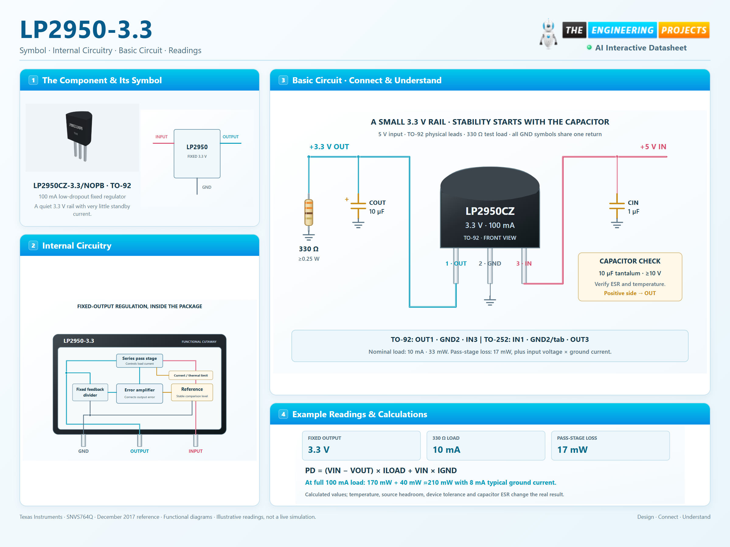
3 stages · Explore one step at a time
TO-92 and TO-252 exchange the IN and OUT pin numbers. The SMD tab belongs to GND.
Place the specified output capacitor close to OUT and GND. Verify effective capacitance and ESR over temperature.
Use PD=(VIN−VOUT)×ILOAD+VIN×IGND. Ground current rises substantially near full load.
Physical TO-92 leads, golden capacitor symbols and shared ground.
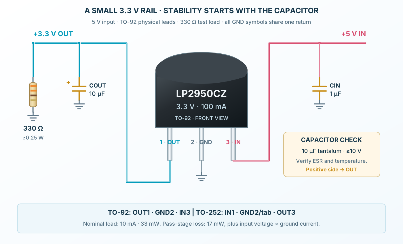
Follow the component values and pin connections
Apply 5 V to IN3 and common return to GND2.
Fit input bypass and the output capacitor with appropriate ESR.
A 330 Ω load draws nominally 10 mA at 3.3 V.
Reference, feedback and protection inside a compact package.
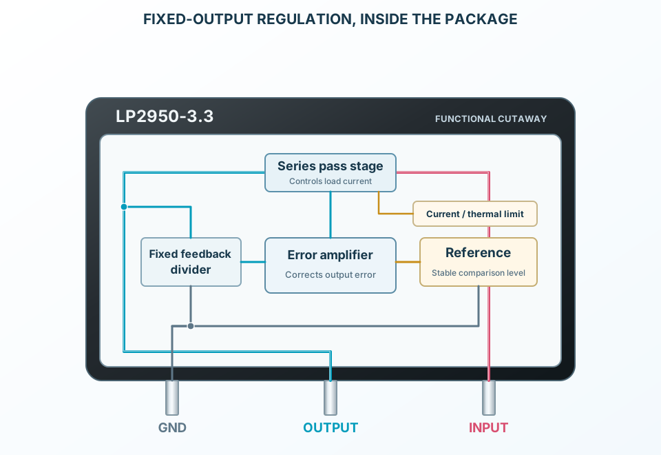
Select a stage to see its role and connections
Compare a fraction of OUT with an internal reference.
Control the series-pass stage to hold the 3.3 V rail.
Current and thermal controls constrain overloads.
Signal names, electrical functions and connection guidance
Scroll within the table to see all columns and rows.
| Pin | Signal | Type | Function & connection |
|---|---|---|---|
| OUT | Regulated rail | Fixed 3.3 V output; an external stability capacitor is required.Connection guidanceConnect to the load and 10 µF output capacitor; return both to GND. TO-92 pin 1; TO-252 pin 3. Use the selected package map. | |
| GND | Common return | Reference and bias-current return for the regulator.Connection guidanceJoin input return, output capacitor and load grounds locally. Pin 2 in both packages; TO-252 exposed tab is also GND. | |
| IN | Supply input | Supply input for the protected series-pass stage.Connection guidanceUse +5 V in the example and local 1 µF bypass. TO-92 pin 3; TO-252 pin 1. Maximum operating input 30 V; allow design margin. |
No pins match these filters. Try another signal name or reset the filters.
C-grade fixed 3.3 V parts
Scroll within the table to see all columns and rows.
| Parameter | Value | Conditions / notes |
|---|---|---|
| Through-hole order | LP2950CZ-3.3/NOPB | TO-92 LP; straight-lead bulk footprint |
| SMD order | LP2950CDT-3.3/NOPB | TO-252 NDP; formed outer leads and grounded tab |
| TO-92 physical pins | OUT1 · GND2 · IN3 | Flat face toward viewer, leads down |
| TO-252 physical pins | IN1 · GND2 · OUT3 | Front face, leads down; tab is GND |
| Accuracy grade | C: ±1% initial | AC-grade values are not substituted |
| Extra controls | No shutdown or error-output lead | These belong to the related LP2951 |
No specifications match. Try a parameter name or a unit.
Verify order suffix and lead form before fabrication.
Temperature and headroom remain essential
Scroll within the table to see all columns and rows.
| Parameter | Value | Conditions / notes |
|---|---|---|
| Nominal output | 3.3 V | Fixed internally; no external divider |
| Recommended input range | 2.3–30 V family range | 3.3 V regulation additionally needs dropout headroom |
| Maximum input stress | 30 V | Do not design at the stress limit |
| Output-current class | 100 mA | Adequate voltage headroom and cooling required |
| Junction operating temperature | −40–125°C | Device junction, not ambient |
| Minimum external load | Not required for LP2950 regulation | Capacitor stability requirements still apply |
No specifications match. Try a parameter name or a unit.
A 2.3 V input cannot produce a regulated 3.3 V output.
3.3 V option; source conditions retained
Scroll within the table to see all columns and rows.
| Parameter | Value | Conditions / notes |
|---|---|---|
| Output at 25°C | 3.267–3.333 V | Nominal 3.3 V |
| Output at −25 to 85°C | 3.251–3.350 V | Manufacturer specified range |
| Output over full temperature | 3.234–3.366 V | −40 to 125°C |
| Across 100 µA–100 mA load | 3.221–3.379 V | Full-temperature limit |
| Temperature coefficient | 50 ppm/°C typical; 150 max. | Output-voltage drift |
| Line regulation at 25°C | 0.04% typical; 0.2% max. | Input from VOUT(nom)+1 V to 30 V |
| Load regulation at 25°C | 0.1% typical; 0.2% max. | Load from 100 µA to 100 mA |
No specifications match. Try a parameter name or a unit.
AC-grade limits are tighter; this page deliberately uses the selected C-grade specification.
Load and temperature change both
Scroll within the table to see all columns and rows.
| Parameter | Value | Conditions / notes |
|---|---|---|
| Dropout at 100 µA load, 25°C | 50 mV typical; 80 mV max. | 150 mV maximum over full temperature |
| Dropout at 100 mA load, 25°C | 380 mV typical; 450 mV max. | 600 mV maximum over full temperature |
| Ground current at 100 µA load | 75 µA typical; 120 µA max. at 25°C | 140 µA maximum over full temperature |
| Ground current at 100 mA load | 8 mA typical; 12 mA max. at 25°C | 14 mA maximum over full temperature |
| Short-circuit current | 160 mA typical; 200 mA max. at 25°C | 220 mA maximum over full temperature; not a load rating |
| Full-load example headroom | At least 0.6 V for the full-temperature dropout limit | Allow additional tolerance and ripple margin |
No specifications match. Try a parameter name or a unit.
Dropout is measured when output falls 100 mV below its nominal operating value.
Capacitance alone is not enough
Scroll within the table to see all columns and rows.
| Parameter | Value | Conditions / notes |
|---|---|---|
| 3.3 V minimum output capacitor | 2.2 µF | Observe the stability-versus-ESR curves |
| Illustrated output capacitor | 10 µF tantalum, ≥10 V | Choose ESR in the recommended stable region across temperature |
| ESR guidance for 2.2 µF | Approximately 0.05–5 Ω | TI application guidance; larger capacitors have their own curves |
| Ceramic output capacitor | May need 0.1–2 Ω series resistance | Use X5R/X7R and check effective capacitance after DC bias |
| Local input bypass | 1 µF | Particularly for batteries or long supply wiring |
| Example COUT polarity | Positive to OUT; negative to GND | Check voltage rating and startup behavior |
No specifications match. Try a parameter name or a unit.
10 µF helps mitigate some startup/short-recovery overshoot. It is not a guarantee for arbitrary source impedance or capacitor ESR.
Manufacturer thermal-board conditions
Scroll within the table to see all columns and rows.
| Parameter | Value | Conditions / notes |
|---|---|---|
| TO-92 θJA | 157.4°C/W | TI reference board; actual assembly varies |
| TO-252 θJA | 51.3°C/W | High-K board with 12 thermal vias |
| TO-252 θJC(bottom) | 2.2°C/W | Grounded exposed tab |
| Total regulator dissipation | (VIN−VOUT)×ILOAD + VIN×IGND | Ground current cannot always be ignored |
| Example 10 mA pass loss | (5−3.3)×0.010 = 17 mW | Add 5×IGND at the actual load |
| Illustrative full-load total | 170 mW + 40 mW = 210 mW | 5 V input, 100 mA load, typical 8 mA ground current |
No specifications match. Try a parameter name or a unit.
Thermal resistance is not an intrinsic promise of available output current.
A modest test load with clear returns
Scroll within the table to see all columns and rows.
| Parameter | Value | Conditions / notes |
|---|---|---|
| Supply / input bypass | 5 V / 1 µF | Common GND return |
| Nominal output | 3.3 V | Actual output follows the C-grade limits |
| Test load | 330 Ω, ≥0.25 W | 3.3/330 = 10 mA |
| Load dissipation | 3.3²/330 = 33 mW | Nominal calculation |
| Output capacitor | 10 µF, ≥10 V, ESR verified | Local placement between OUT and GND |
| Pass-stage loss | 17 mW | Does not include load-dependent ground current |
No specifications match. Try a parameter name or a unit.
Calculated illustration; not measured waveforms or an executable simulation.
No matching rowsTry a pin name, parameter, unit or test condition, or reset the filters.
Supply low-current electronics with modest dropout and low light-load bias.
Manufacturer application guideUse the reference accuracy and a stable output network for appropriate analog loads.
Manufacturer application guideConsider total system leakage and the regulator ground current at the actual load.
Manufacturer application guideFind LP2950-3.3 in the Components Library to place its schematic symbol and connect its pins.
Reference page · circuit simulation model not yet availableOpen ProTech