MAX232RS-232 transceiver
Connect your microcontroller’s logic to the serial world.
MAX232 is a 16-pin serial interface IC that connects a microcontroller’s TTL/CMOS logic to an RS-232 device. Two transmitters and two receivers translate and invert the signals in both directions. It runs from a single 5 V supply; a charge pump and four external capacitors generate the driver’s positive and negative rails.

Simulate the MAX232 in ProTech
MAX232: RS-232 level translator — the working circuit from our online simulator, running on this page.
- 1 · RunPress the green Run button in the simulator's bottom bar. The circuit solves live.
- 2 · Click the partWhile it runs, click the MAX232 on the sheet: its pop-up opens with live readings, dials and the datasheet.
- 3 · ExperimentUse the pop-up's Lab and Check pages, the oscilloscope and the voltmeters; Stop to edit any property.
16Physical pins
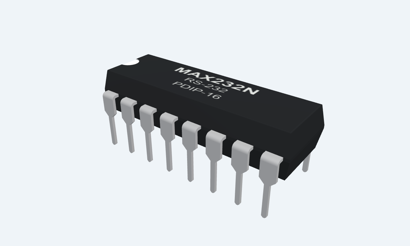
MAX232NPDIP-16
Manufacturer-referencedTexas Instruments
Pin diagram
Select a pin to explore its connection
Highlight
MAX232NPDIP-16The notch marks the top; pin 1 is at the upper left.
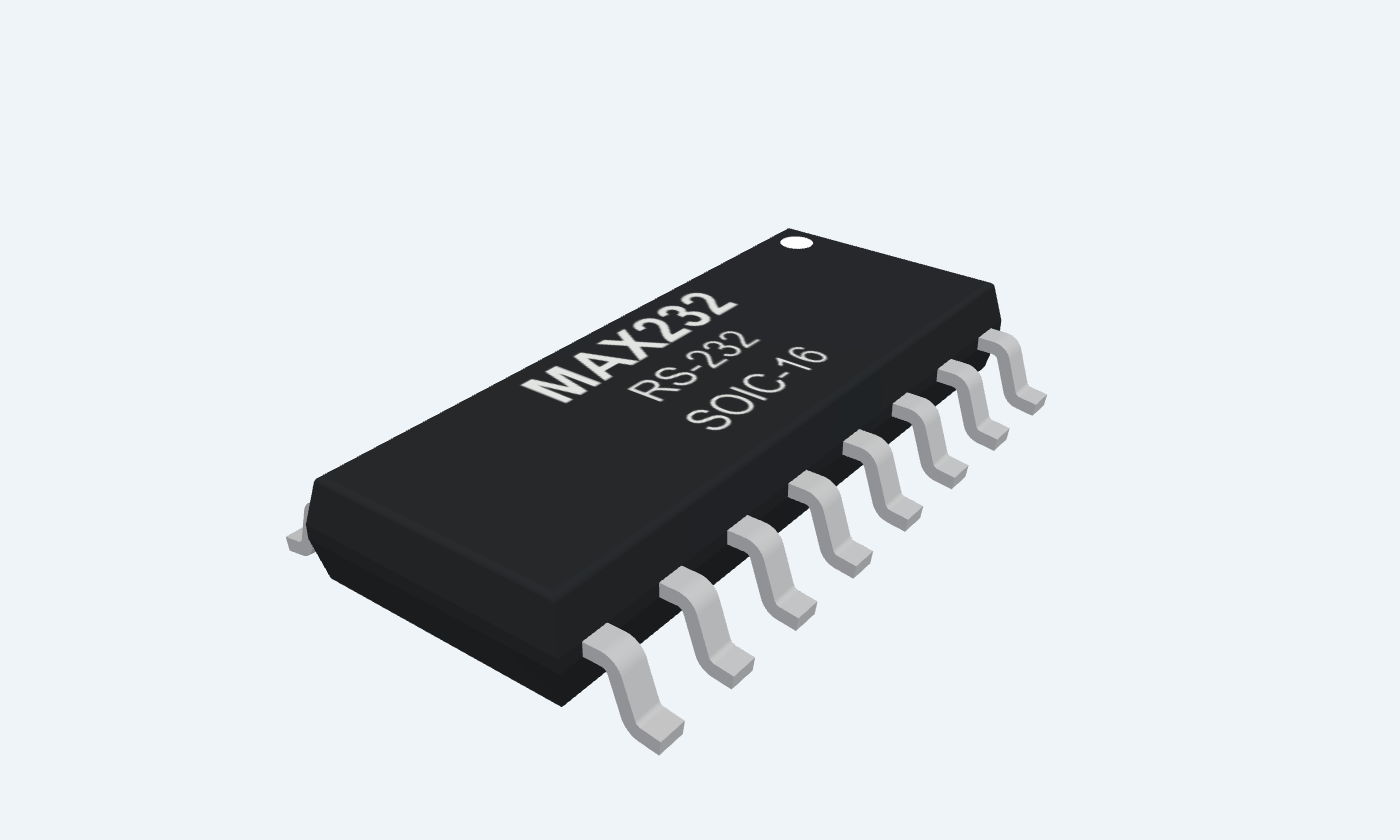
MAX232DSOIC-16The dot identifies pin 1 at the upper left.
Click a lead or use the arrow keys. The notch marks the top; pin 1 is at the upper left.
PIN 1 · Charge pump
CapacitorC1+
Function
Positive connection of the flying capacitor C1.
How to connect
Connect C1 (1 µF) between pins 1 and 3; positive terminal to pin 1 if polarized.
Electrical note
Use 1 µF flying capacitors for this MAX232. Ceramic capacitors avoid polarity concerns; follow the marked +/− connections for polarized parts.
PIN 2 · Charge pump
OutputVS+
Function
Positive voltage reservoir of the internal charge pump.
How to connect
Connect the positive reservoir capacitor as shown in the manufacturer’s typical application. This is not a general-purpose supply.
Electrical note
Positive charge-pump reservoir. Use it for the reservoir capacitor, not as an external power output.
PIN 3 · Charge pump
CapacitorC1−
Function
Negative connection of the flying capacitor C1.
How to connect
Connect to the other side of C1 at pin 1.
Electrical note
Use 1 µF flying capacitors for this MAX232. Ceramic capacitors avoid polarity concerns; follow the marked +/− connections for polarized parts.
PIN 4 · Charge pump
CapacitorC2+
Function
Positive connection of the inverting capacitor C2.
How to connect
Connect C2 (1 µF) between pins 4 and 5; positive terminal to pin 4 if polarized.
Electrical note
Use 1 µF flying capacitors for this MAX232. Ceramic capacitors avoid polarity concerns; follow the marked +/− connections for polarized parts.
PIN 5 · Charge pump
CapacitorC2−
Function
Negative connection of the inverting capacitor C2.
How to connect
Connect to the other side of C2 at pin 4.
Electrical note
Use 1 µF flying capacitors for this MAX232. Ceramic capacitors avoid polarity concerns; follow the marked +/− connections for polarized parts.
PIN 6 · Charge pump
OutputVS−
Function
Negative voltage reservoir of the internal charge pump.
How to connect
Connect the negative reservoir capacitor to ground; observe capacitor polarity. Not a general-purpose supply.
Electrical note
Negative charge-pump reservoir. For a polarized reservoir capacitor, the positive terminal goes to ground.
PIN 7 · RS-232
OutputT2OUT
Function
Channel 2 transmit output at RS-232 voltage levels.
How to connect
Connect to the remote receiver. Inverts the logic applied to T2IN (pin 10).
Electrical note
Bipolar RS-232 output. Typical levels are about ±7 V at 5 V supply, 25 °C and a 3 kΩ load. Keep it off microcontroller GPIO inputs.
PIN 8 · RS-232
InputR2IN
Function
Channel 2 receive input from an RS-232 line.
How to connect
Connect to the remote transmitter. Its converted logic appears at R2OUT (pin 9).
Electrical note
RS-232 input only; specified input range is −30 to +30 V. The paired logic output is inverted.
PIN 9 · TTL / CMOS
OutputR2OUT
Function
Channel 2 receive output at TTL/CMOS logic levels.
How to connect
Connect to the local UART receive input; paired with R2IN (pin 8).
Electrical note
Logic-level output for the local UART. A negative RS-232 input produces HIGH; a positive input produces LOW.
PIN 10 · TTL / CMOS
InputT2IN
Function
Channel 2 transmit input from TTL/CMOS logic.
How to connect
Connect to the local UART transmit output; paired with T2OUT (pin 7).
Electrical note
LOW: 0.8 V or below. HIGH: 2 V or above. The paired RS-232 output is inverted; do not apply RS-232 voltage to this logic input.
PIN 11 · TTL / CMOS
InputT1IN
Function
Channel 1 transmit input from TTL/CMOS logic.
How to connect
Connect to the local UART transmit output; paired with T1OUT (pin 14).
Electrical note
LOW: 0.8 V or below. HIGH: 2 V or above. The paired RS-232 output is inverted; do not apply RS-232 voltage to this logic input.
PIN 12 · TTL / CMOS
OutputR1OUT
Function
Channel 1 receive output at TTL/CMOS logic levels.
How to connect
Connect to the local UART receive input; paired with R1IN (pin 13).
Electrical note
Logic-level output for the local UART. A negative RS-232 input produces HIGH; a positive input produces LOW.
PIN 13 · RS-232
InputR1IN
Function
Channel 1 receive input from an RS-232 line.
How to connect
Connect to the remote transmitter; paired with R1OUT (pin 12).
Electrical note
RS-232 input only; specified input range is −30 to +30 V. The paired logic output is inverted.
PIN 14 · RS-232
OutputT1OUT
Function
Channel 1 transmit output at RS-232 voltage levels.
How to connect
Connect to the remote receiver. Inverts the logic applied to T1IN (pin 11).
Electrical note
Bipolar RS-232 output. Typical levels are about ±7 V at 5 V supply, 25 °C and a 3 kΩ load. Keep it off microcontroller GPIO inputs.
PIN 15 · Ground
GroundGND
Function
Common ground reference for logic and the transceiver.
How to connect
Connect to circuit ground and the serial connector’s signal ground.
Electrical note
0 V reference. Connect the local logic ground and the remote interface’s signal ground.
PIN 16 · Supply
SupplyVCC
Function
Positive supply input: 5 V nominal.
How to connect
Use a regulated 4.5–5.5 V supply. Place the supply bypass capacitor close to VCC and GND.
Electrical note
5 V nominal; keep the supply within 4.5–5.5 V. Use a common supply with the connected logic circuit.
Key specifications
The charge pump creates the positive and negative voltages RS-232 needs, using a single 5 V supply.
Nominal supply5 V
Maximum data rate120 kbit/s
Ambient range0–70 °C
Each pump capacitor1 µF
Package details
MAX232N · PDIP-16
| Property | Details |
|---|---|
| Manufacturer | Texas Instruments |
| Part number | MAX232N |
| Package | PDIP-16 |
| Connections | 16 pins |
| Mounting | Through-hole |
| Lead pitch | 2.54 mm |
| Package code | N |
| Thermal reference | 60.6 °C/W |
Electrical & physical specifications
Texas Instruments MAX232N · PDIP-16 · Reference values
Manufacturer specifications 14 parameters
Scroll sideways to see all columns.
| Parameter | Value | Conditions / notes |
|---|---|---|
| Supply voltage | 4.5–5.5 V | 5 V nominal; recommended operating range |
| Maximum data rate | 120 kbit/s | One transmitter output switching; see datasheet test conditions |
| Transmit / receive channels | 2 / 2 | Two drivers and two receivers |
| Supply current | 8 mA typ. / 10 mA max. | VCC = 5.5 V, outputs open, ambient = 25 °C |
| Driver output | +7 V / −7 V typical | VCC = 5 V, ambient = 25 °C, 3 kΩ load to GND; +5 V / −5 V guaranteed limits |
| Logic input HIGH / LOW | ≥ 2 V / ≤ 0.8 V | T1IN and T2IN; values between thresholds are undefined |
| Receiver input range | −30 to +30 V | R1IN and R2IN only |
| Receiver hysteresis | 0.5 V typical | At VCC = 5 V |
| Operating temperature | 0 to +70 °C | MAX232N commercial grade; MAX232I has a different range |
| Charge-pump capacitors | 4 × 1 µF | Plus supply bypass; follow the typical application, section 8 |
| Package | PDIP-16, 16 leads | TI N package; 2.54 mm lead pitch |
| Junction-to-ambient | 60.6 °C/W | PDIP-16; datasheet thermal characterization conditions |
| Supply absolute maximum | −0.3 to +6 V | Stress rating only, not an operating range |
| Maximum junction temperature | 150 °C | Absolute maximum, not the ambient operating rating |
No specifications match. Try a parameter name or a unit.
Reference: TI SLLS047N, sections 4–8 and package drawings. Check the exact manufacturer and suffix before substituting MAX232A, MAX3232 or another family member. Verify a production footprint against your ordered part.
Connections by function
Select a pin for its function, connection guidance and electrical notes.
Charge pump6 pins
RS-2324 pins
TTL / CMOS4 pins
Ground1 pin
Supply1 pin
Charge pump6 pins
RS-2324 pins
TTL / CMOS4 pins
Ground1 pin
Supply1 pin
MAX232 at a glance
Follow the labeled connections and functional stages
How it works
5 stages · Explore one step at a time
Two electrical languages
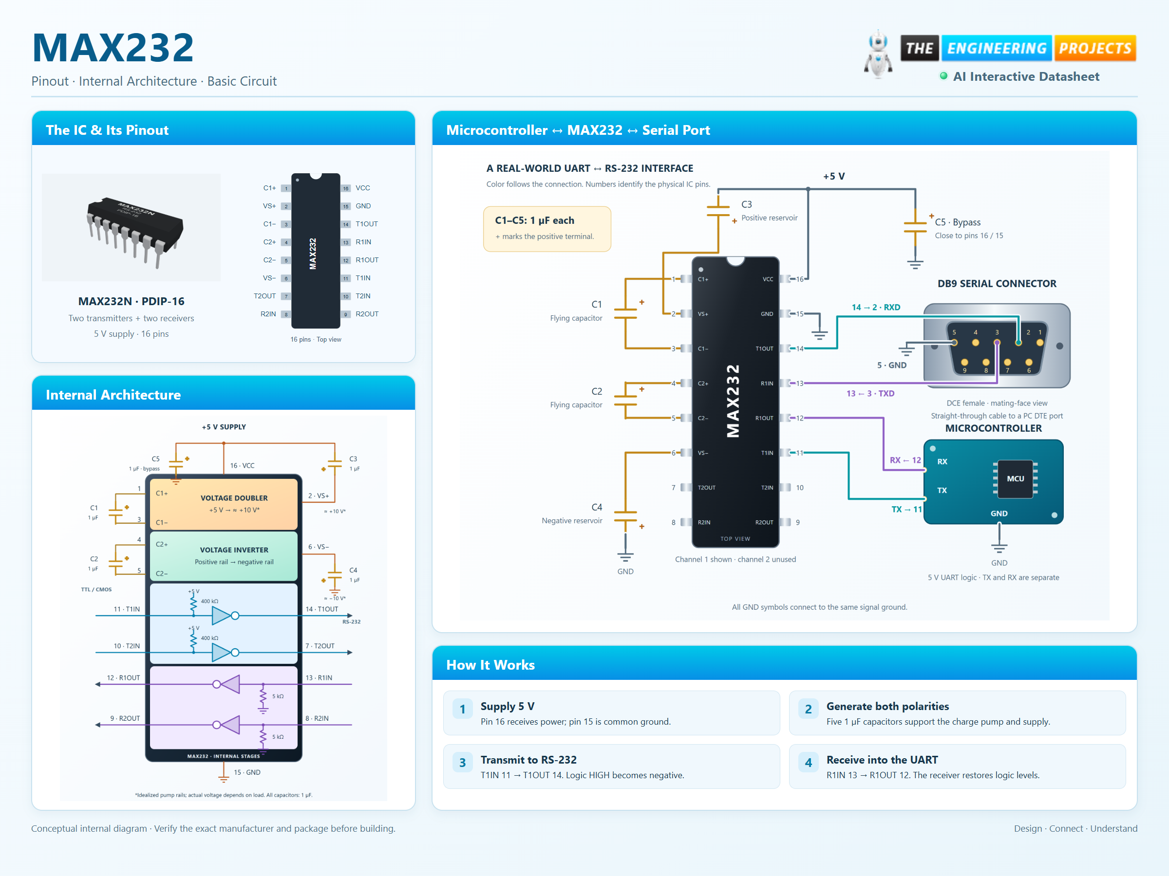
A microcontroller’s UART uses logic levels, while an RS-232 port uses positive and negative voltages. The MAX232 translates between them. It changes voltage levels and polarity; it does not create a baud rate or decode the data.
Create the driver rails
Connect pin 16 to 5 V and pin 15 to ground. C1 transfers charge in the voltage doubler; C2 supports the inverter. C3 and C4 hold the positive and negative rails, and C5 bypasses the supply. This MAX232 circuit uses 1 µF for all five capacitors.
The diagram’s approximately ±10 V rails explain the unloaded charge-pump action. Actual rails and output swing depend on supply, load and losses.
Transmit to RS-232
Microcontroller TX feeds T1IN, pin 11. T1OUT, pin 14, drives the serial line with an inverted bipolar signal: logic HIGH becomes a negative RS-232 voltage, and logic LOW becomes positive. Channel 2 works the same way through pins 10 and 7.
Receive into the UART
The remote transmitter reaches R1IN, pin 13. The receiver converts the RS-232 signal into a logic output at R1OUT, pin 12, for the microcontroller’s RX input. A negative input gives logic HIGH; a positive input gives LOW. The second receiver uses pins 8 and 9.
Complete the connection
The Basic Circuit shows a DCE female DB9 connector from its mating face: pin 2 carries the MAX232’s output, pin 3 accepts the PC’s transmit signal, and pin 5 is signal ground. A straight-through cable joins it to a PC DTE port. TX and RX operate independently, allowing two-way communication.
Step 1 of 5
Follow the signal
Choose a channel, change its input and read the output polarity.
Transmitter 1
Converts the local logic output into an inverted bipolar RS-232 signal.
Set the input
Input
T1IN · pin 11 · TTL / CMOS
HIGHLogic levelMAX232Inverting driver
Output
T1OUT · pin 14 · RS-232
NEGATIVERS-232 polarityA HIGH logic input produces a negative RS-232 output. A LOW input produces a positive output.
Transmitter 2
A second independent transmit path, powered by the same internal charge pump.
Set the input
Input
T2IN · pin 10 · TTL / CMOS
HIGHLogic levelMAX232Inverting driver
Output
T2OUT · pin 7 · RS-232
NEGATIVERS-232 polarityA HIGH logic input produces a negative RS-232 output. A LOW input produces a positive output.
Receiver 1
Accepts an RS-232 line signal and provides an inverted logic-level output for the local UART.
Set the input
Input
R1IN · pin 13 · RS-232
POSITIVERS-232 polarityMAX232Inverting receiver
Output
R1OUT · pin 12 · TTL / CMOS
LOWLogic levelA positive RS-232 input produces a LOW logic output. A negative input produces a HIGH output.
Receiver 2
The second receive path works independently of receiver 1. Both use the common ground reference.
Set the input
Input
R2IN · pin 8 · RS-232
POSITIVERS-232 polarityMAX232Inverting receiver
Output
R2OUT · pin 9 · TTL / CMOS
LOWLogic levelA positive RS-232 input produces a LOW logic output. A negative input produces a HIGH output.
MAX232 in a circuit
5 V supply · Charge-pump capacitors · UART ↔ RS-232
Trace wiring
Connect it, step by step
Follow the component values and pin connections
Power first
Pin 16 → regulated 5 V. Pin 15 → common ground. Put a 1 µF bypass close to these pins.
- Regulated +5 V
- VCC · pin 16
- Signal ground
- GND · pin 15, MCU & DB9 pin 5
- C5 · 1 µF bypass
- VCC ↔ GND, close to the IC
Add the charge pump
C1: 1–3. C2: 4–5. C3: 2–VCC. C4: GND–6. All are 1 µF; the + signs show polarized-capacitor orientation.
- C1 · 1 µF
- Pin 1 (+) ↔ pin 3 (−)
- C2 · 1 µF
- Pin 4 (+) ↔ pin 5 (−)
- C3 · 1 µF
- Pin 2 (+) ↔ VCC (−)
- C4 · 1 µF
- GND (+) ↔ pin 6 (−)
Connect the local UART
TX → T1IN (11). RX ← R1OUT (12). These are the logic-side connections.
- MCU TX
- T1IN · pin 11
- R1OUT · pin 12
- MCU RX
Connect the remote interface
T1OUT (14) → DB9 pin 2. DB9 pin 3 → R1IN (13). Pin 5 → common ground. This DCE female connector uses a straight-through cable to a PC’s DTE port.
- T1OUT · pin 14
- DB9 pin 2 · PC receive
- DB9 pin 3 · PC transmit
- R1IN · pin 13
- DB9 pin 5
- Common signal ground
Use the second channel in the same way: T2IN (10) → T2OUT (7), and R2IN (8) → R2OUT (9).
C3 may return to VCC or ground; this guide uses VCC, matching the featured circuit. Ceramic capacitors are acceptable. Follow the datasheet for the exact part and layout.
Inside MAX232
Charge pump · Line drivers · Line receivers
Explore the circuit
Select a stage to see its role and connections
Charge pump
The first switched-capacitor stage doubles the 5 V supply. The second stage inverts that positive rail, giving the transmitters both polarities from one supply. C1 and C2 transfer charge; C3 and C4 store it. C5 keeps the supply stable.
- Flying capacitors
- C1: pins 1–3 · C2: pins 4–5
- Reservoir capacitors
- VS+: pin 2 · VS−: pin 6
- External parts
- Five 1 µF capacitors, including supply bypass
- Driver rails
- Approximately +10 V and −10 V are idealized values. Real rails and output swing drop under load.
Transmitter 1
Converts the local logic output into an inverted bipolar RS-232 signal.
InputT1IN · pin 11 · TTL / CMOS
OutputT1OUT · pin 14 · RS-232
This stage inverts the signal polarity.
Transmitter 2
A second independent transmit path, powered by the same internal charge pump.
InputT2IN · pin 10 · TTL / CMOS
OutputT2OUT · pin 7 · RS-232
This stage inverts the signal polarity.
Receiver 1
Accepts an RS-232 line signal and provides an inverted logic-level output for the local UART.
InputR1IN · pin 13 · RS-232
OutputR1OUT · pin 12 · TTL / CMOS
This stage inverts the signal polarity.
Receiver 2
The second receive path works independently of receiver 1. Both use the common ground reference.
InputR2IN · pin 8 · RS-232
OutputR2OUT · pin 9 · TTL / CMOS
This stage inverts the signal polarity.
Input resistance and reference details
The 400 kΩ pullups and 5 kΩ receiver loads show the internal equivalent in Maxim’s reference diagram. They are not extra parts you need to connect.
Selected packagePDIP-16MAX232N
Physical connections16 pinsPackage-specific numbering
Reference collection2 tables14 parameters & pin functions
Pin reference
Signal names, electrical functions and connection guidance
Physical pin numbers16 pins
Scroll within the table to see all columns and rows.
| Pin | Signal | Type | Function & connection |
|---|---|---|---|
| C1+ | Capacitor | Positive connection of the flying capacitor C1.Connection guidanceConnect C1 (1 µF) between pins 1 and 3; positive terminal to pin 1 if polarized. Use 1 µF flying capacitors for this MAX232. Ceramic capacitors avoid polarity concerns; follow the marked +/− connections for polarized parts. | |
| VS+ | Output | Positive voltage reservoir of the internal charge pump.Connection guidanceConnect the positive reservoir capacitor as shown in the manufacturer’s typical application. This is not a general-purpose supply. Positive charge-pump reservoir. Use it for the reservoir capacitor, not as an external power output. | |
| C1− | Capacitor | Negative connection of the flying capacitor C1.Connection guidanceConnect to the other side of C1 at pin 1. Use 1 µF flying capacitors for this MAX232. Ceramic capacitors avoid polarity concerns; follow the marked +/− connections for polarized parts. | |
| C2+ | Capacitor | Positive connection of the inverting capacitor C2.Connection guidanceConnect C2 (1 µF) between pins 4 and 5; positive terminal to pin 4 if polarized. Use 1 µF flying capacitors for this MAX232. Ceramic capacitors avoid polarity concerns; follow the marked +/− connections for polarized parts. | |
| C2− | Capacitor | Negative connection of the inverting capacitor C2.Connection guidanceConnect to the other side of C2 at pin 4. Use 1 µF flying capacitors for this MAX232. Ceramic capacitors avoid polarity concerns; follow the marked +/− connections for polarized parts. | |
| VS− | Output | Negative voltage reservoir of the internal charge pump.Connection guidanceConnect the negative reservoir capacitor to ground; observe capacitor polarity. Not a general-purpose supply. Negative charge-pump reservoir. For a polarized reservoir capacitor, the positive terminal goes to ground. | |
| T2OUT | Output | Channel 2 transmit output at RS-232 voltage levels.Connection guidanceConnect to the remote receiver. Inverts the logic applied to T2IN (pin 10). Bipolar RS-232 output. Typical levels are about ±7 V at 5 V supply, 25 °C and a 3 kΩ load. Keep it off microcontroller GPIO inputs. | |
| R2IN | Input | Channel 2 receive input from an RS-232 line.Connection guidanceConnect to the remote transmitter. Its converted logic appears at R2OUT (pin 9). RS-232 input only; specified input range is −30 to +30 V. The paired logic output is inverted. | |
| R2OUT | Output | Channel 2 receive output at TTL/CMOS logic levels.Connection guidanceConnect to the local UART receive input; paired with R2IN (pin 8). Logic-level output for the local UART. A negative RS-232 input produces HIGH; a positive input produces LOW. | |
| T2IN | Input | Channel 2 transmit input from TTL/CMOS logic.Connection guidanceConnect to the local UART transmit output; paired with T2OUT (pin 7). LOW: 0.8 V or below. HIGH: 2 V or above. The paired RS-232 output is inverted; do not apply RS-232 voltage to this logic input. | |
| T1IN | Input | Channel 1 transmit input from TTL/CMOS logic.Connection guidanceConnect to the local UART transmit output; paired with T1OUT (pin 14). LOW: 0.8 V or below. HIGH: 2 V or above. The paired RS-232 output is inverted; do not apply RS-232 voltage to this logic input. | |
| R1OUT | Output | Channel 1 receive output at TTL/CMOS logic levels.Connection guidanceConnect to the local UART receive input; paired with R1IN (pin 13). Logic-level output for the local UART. A negative RS-232 input produces HIGH; a positive input produces LOW. | |
| R1IN | Input | Channel 1 receive input from an RS-232 line.Connection guidanceConnect to the remote transmitter; paired with R1OUT (pin 12). RS-232 input only; specified input range is −30 to +30 V. The paired logic output is inverted. | |
| T1OUT | Output | Channel 1 transmit output at RS-232 voltage levels.Connection guidanceConnect to the remote receiver. Inverts the logic applied to T1IN (pin 11). Bipolar RS-232 output. Typical levels are about ±7 V at 5 V supply, 25 °C and a 3 kΩ load. Keep it off microcontroller GPIO inputs. | |
| GND | Ground | Common ground reference for logic and the transceiver.Connection guidanceConnect to circuit ground and the serial connector’s signal ground. 0 V reference. Connect the local logic ground and the remote interface’s signal ground. | |
| VCC | Supply | Positive supply input: 5 V nominal.Connection guidanceUse a regulated 4.5–5.5 V supply. Place the supply bypass capacitor close to VCC and GND. 5 V nominal; keep the supply within 4.5–5.5 V. Use a common supply with the connected logic circuit. |
No pins match these filters. Try another signal name or reset the filters.
Electrical & physical specifications
Texas Instruments MAX232N · PDIP-16 · Reference values
Manufacturer-referenced values14 parameters
Scroll within the table to see all columns and rows.
| Parameter | Value | Conditions / notes |
|---|---|---|
| Supply voltage | 4.5–5.5 V | 5 V nominal; recommended operating range |
| Maximum data rate | 120 kbit/s | One transmitter output switching; see datasheet test conditions |
| Transmit / receive channels | 2 / 2 | Two drivers and two receivers |
| Supply current | 8 mA typ. / 10 mA max. | VCC = 5.5 V, outputs open, ambient = 25 °C |
| Driver output | +7 V / −7 V typical | VCC = 5 V, ambient = 25 °C, 3 kΩ load to GND; +5 V / −5 V guaranteed limits |
| Logic input HIGH / LOW | ≥ 2 V / ≤ 0.8 V | T1IN and T2IN; values between thresholds are undefined |
| Receiver input range | −30 to +30 V | R1IN and R2IN only |
| Receiver hysteresis | 0.5 V typical | At VCC = 5 V |
| Operating temperature | 0 to +70 °C | MAX232N commercial grade; MAX232I has a different range |
| Charge-pump capacitors | 4 × 1 µF | Plus supply bypass; follow the typical application, section 8 |
| Package | PDIP-16, 16 leads | TI N package; 2.54 mm lead pitch |
| Junction-to-ambient | 60.6 °C/W | PDIP-16; datasheet thermal characterization conditions |
| Supply absolute maximum | −0.3 to +6 V | Stress rating only, not an operating range |
| Maximum junction temperature | 150 °C | Absolute maximum, not the ambient operating rating |
No specifications match. Try a parameter name or a unit.
Reference: TI SLLS047N, sections 4–8 and package drawings. Check the exact manufacturer and suffix before substituting MAX232A, MAX3232 or another family member. Verify a production footprint against your ordered part.
No matching rowsTry a pin name, parameter, unit or test condition, or reset the filters.
Build a UART-to-RS-232 interface
Route UART TX to T1IN (11), then T1OUT (14) to the remote receiver. Bring the remote transmit line into R1IN (13), with R1OUT (12) returning to UART RX.
Use a common signal ground. Check the remote connector’s DTE/DCE pin assignment.
Manufacturer application guideGet the charge pump right
Use the four 1 µF pump capacitors and a local supply bypass as shown in the reference circuit. Keep these connections short and check polarity when using polarized capacitors.
VS+ and VS− serve the charge pump; they are not supply rails for other components.
Manufacturer application guideTake it into ProTech
Find MAX232 in the Components Library to place its schematic symbol and connect its pins.
Schematic available · Simulation model pendingOpen ProTech