MAX7219Eight-digit serial LED driver
Three control wires. Eight digits. A display that refreshes itself.
MAX7219 combines an eight-digit LED driver, display memory and a serial interface in one 24-pin IC. It can control eight common-cathode seven-segment digits or 64 individual LEDs, refreshing the display while the host performs other work. A 16-bit command selects a digit or control register. Code-B decoding handles numbers and a small set of characters; raw segment mode gives direct control of each LED. RSET establishes peak current, while a separate intensity register adjusts PWM brightness. This page uses the industrial-temperature MAX7219ENG+ and MAX7219EWG+ packages with the same pin numbering. The example uses a 5 V host, eight red digits, both ground returns and local bypass capacitors. The MAX7219 clocks data regardless of LOAD, so it must not be treated as a MAX7221 with a clock-gating chip select.
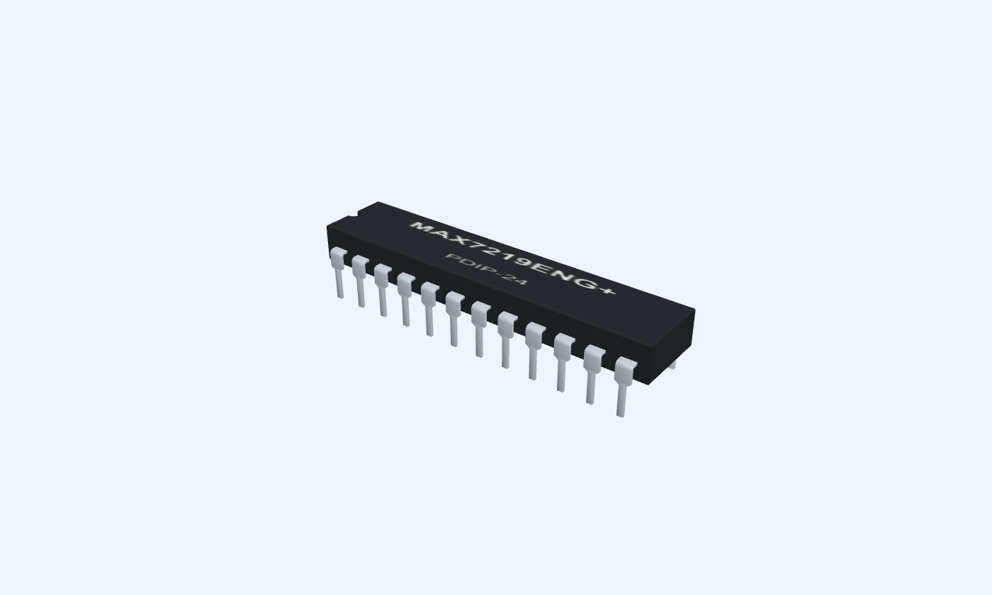
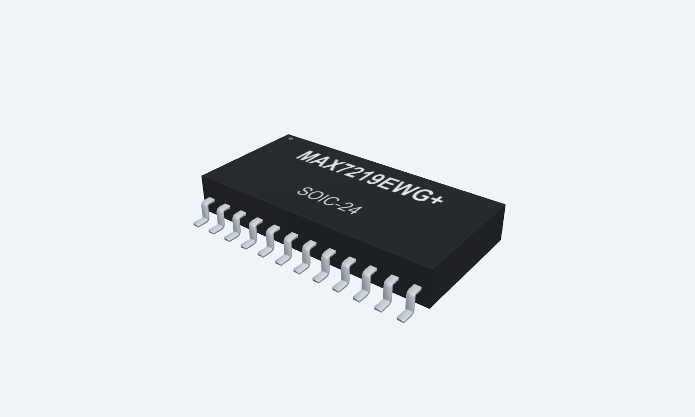

24Physical pins
MAX7219ENG+PDIP-24
Manufacturer-referencedAnalog Devices
Pin diagram
Select a pin to explore its connection
Highlight
MAX7219PDIP-24Top view
MAX7219SOIC-24Top view
Click a lead or use the arrow keys. Top view
PIN 1 · Serial controls
InputDIN
Function
Accepts serial data on each rising CLK edge.
How to connect
Connect to a 5 V host MOSI output.
Electrical note
A guaranteed HIGH requires at least 3.5 V; use level translation with a 3.3 V host.
PIN 2 · Digit cathodes
Current sinkDIG0
Function
Selects digit 0 by sinking its common-cathode current.
How to connect
Connect to the common cathode of display digit 0.
Electrical note
Inactive digit outputs are driven HIGH on MAX7219, not high impedance.
PIN 3 · Digit cathodes
Current sinkDIG4
Function
Selects digit 4 by sinking its common-cathode current.
How to connect
Connect to the common cathode of display digit 4.
Electrical note
Inactive digit outputs are driven HIGH on MAX7219, not high impedance.
PIN 4 · Ground
GroundGND
Function
Supply and LED-current return.
How to connect
Connect both ground pins to the common return.
PIN 5 · Digit cathodes
Current sinkDIG6
Function
Selects digit 6 by sinking its common-cathode current.
How to connect
Connect to the common cathode of display digit 6.
Electrical note
Inactive digit outputs are driven HIGH on MAX7219, not high impedance.
PIN 6 · Digit cathodes
Current sinkDIG2
Function
Selects digit 2 by sinking its common-cathode current.
How to connect
Connect to the common cathode of display digit 2.
Electrical note
Inactive digit outputs are driven HIGH on MAX7219, not high impedance.
PIN 7 · Digit cathodes
Current sinkDIG3
Function
Selects digit 3 by sinking its common-cathode current.
How to connect
Connect to the common cathode of display digit 3.
Electrical note
Inactive digit outputs are driven HIGH on MAX7219, not high impedance.
PIN 8 · Digit cathodes
Current sinkDIG7
Function
Selects digit 7 by sinking its common-cathode current.
How to connect
Connect to the common cathode of display digit 7.
Electrical note
Inactive digit outputs are driven HIGH on MAX7219, not high impedance.
PIN 9 · Ground
GroundGND
Function
Supply and LED-current return.
How to connect
Connect both ground pins to the common return.
PIN 10 · Digit cathodes
Current sinkDIG5
Function
Selects digit 5 by sinking its common-cathode current.
How to connect
Connect to the common cathode of display digit 5.
Electrical note
Inactive digit outputs are driven HIGH on MAX7219, not high impedance.
PIN 11 · Digit cathodes
Current sinkDIG1
Function
Selects digit 1 by sinking its common-cathode current.
How to connect
Connect to the common cathode of display digit 1.
Electrical note
Inactive digit outputs are driven HIGH on MAX7219, not high impedance.
PIN 12 · Serial controls
InputLOAD
Function
A rising edge transfers the last 16 serial bits to the selected register.
How to connect
Hold LOW during each 16-bit transfer, then pulse HIGH.
Electrical note
CLK still shifts the MAX7219 while LOAD is HIGH; this differs from MAX7221 chip-select behavior.
PIN 13 · Serial controls
InputCLK
Function
Serial clock: DIN shifts on rising edges and DOUT changes after falling edges.
How to connect
Connect to host clock; maximum serial clock is 10 MHz.
PIN 14 · Segment anodes
Current sourceSEG A
Function
Supplies the A segment anodes.
How to connect
Join the A anodes across all eight common-cathode digits.
Electrical note
Peak current is set by RSET; digit multiplexing and intensity PWM determine average current.
PIN 15 · Segment anodes
Current sourceSEG F
Function
Supplies the F segment anodes.
How to connect
Join the F anodes across all eight common-cathode digits.
Electrical note
Peak current is set by RSET; digit multiplexing and intensity PWM determine average current.
PIN 16 · Segment anodes
Current sourceSEG B
Function
Supplies the B segment anodes.
How to connect
Join the B anodes across all eight common-cathode digits.
Electrical note
Peak current is set by RSET; digit multiplexing and intensity PWM determine average current.
PIN 17 · Segment anodes
Current sourceSEG G
Function
Supplies the G segment anodes.
How to connect
Join the G anodes across all eight common-cathode digits.
Electrical note
Peak current is set by RSET; digit multiplexing and intensity PWM determine average current.
PIN 18 · Current setting
Analog referenceISET
Function
Sets the peak segment current through an external resistor.
How to connect
Connect RSET to V+; the example uses 64.9 kΩ for a low-current red display.
Electrical note
Choose RSET from the manufacturer table using LED forward voltage; do not leave it unconnected.
PIN 19 · Supply
SupplyV+
Function
Powers the serial logic, memory and display drivers.
How to connect
Use 5 V with 100 nF ceramic and 10 µF bulk bypass near the IC.
Electrical note
Operating supply range: 4.0–5.5 V.
PIN 20 · Segment anodes
Current sourceSEG C
Function
Supplies the C segment anodes.
How to connect
Join the C anodes across all eight common-cathode digits.
Electrical note
Peak current is set by RSET; digit multiplexing and intensity PWM determine average current.
PIN 21 · Segment anodes
Current sourceSEG E
Function
Supplies the E segment anodes.
How to connect
Join the E anodes across all eight common-cathode digits.
Electrical note
Peak current is set by RSET; digit multiplexing and intensity PWM determine average current.
PIN 22 · Segment anodes
Current sourceSEG DP
Function
Supplies the decimal point segment anodes.
How to connect
Join the DP anodes across all eight common-cathode digits.
Electrical note
Peak current is set by RSET; digit multiplexing and intensity PWM determine average current.
PIN 23 · Segment anodes
Current sourceSEG D
Function
Supplies the D segment anodes.
How to connect
Join the D anodes across all eight common-cathode digits.
Electrical note
Peak current is set by RSET; digit multiplexing and intensity PWM determine average current.
PIN 24 · Serial controls
OutputDOUT
Function
Serial data output for daisy-chaining another driver.
How to connect
Connect to the next DIN, or leave open for one IC.
Electrical note
Never high impedance; do not connect directly to a shared MISO bus.
Key specifications
Eight display bytes remain in internal RAM. A scan engine selects one digit at a time, and the segment drivers supply the requested anodes. Brightness combines the RSET current setting with intensity PWM.
Display capacity8 digits / 64 LEDs
Operating supply4.0–5.5 V
Serial clock10 MHz maximum
PWM levels16 intensity settings
Package details
MAX7219ENG+ · PDIP-24
| Property | Details |
|---|---|
| Manufacturer | Analog Devices |
| Part number | MAX7219ENG+ |
| Package | PDIP-24 |
| Connections | 24 pins |
| Mounting | Through-hole |
| Lead pitch | 2.54 mm |
| Package code | PDIP-24 |
| Thermal reference | See operating and package limits |
Supply and logic levels
Recommended operating conditions
Manufacturer specifications 7 parameters
Scroll sideways to see all columns.
| Parameter | Value | Conditions / notes |
|---|---|---|
| V+ operating range | 4.0–5.5 V | Example uses regulated 5 V |
| Input HIGH / LOW | ≥3.5 V / ≤0.8 V | DIN, CLK and LOAD; 3.3 V is not a guaranteed HIGH |
| Shutdown current | 150 µA typical | 25°C, logic inputs at a supply rail |
| Display refresh | 800 Hz typical at eight digits | 500–1300 Hz specified scan range |
| Selected E temperature grade | −40 to +85°C | C grade is 0–70°C |
| Bypass capacitors | 100 nF ceramic + 10 µF bulk | Close to V+19 and ground |
| Ground contacts | Pins 4 and 9 | Connect both; carry multiplexed display return current |
No specifications match. Try a parameter name or a unit.
Check power dissipation separately from the temperature grade.
Registers and command words
16 bits, MSB first: address byte then data byte
Manufacturer specifications 8 parameters
Scroll sideways to see all columns.
| Parameter | Value | Conditions / notes |
|---|---|---|
| 0x00 · No-op | Data ignored | Use to pass a command through a daisy chain |
| 0x01–0x08 · Digits | One display byte each | Addresses correspond to DIG0–DIG7 |
| 0x09 · Decode mode | One bit per digit | 1 enables Code B; 0 selects raw segments |
| 0x0A · Intensity | Low nibble 0x0–0xF | 16 PWM settings |
| 0x0B · Scan limit | 0–7 | Selects one through eight scanned digits |
| 0x0C · Shutdown | 0=blank / 1=normal | RAM and control contents retained |
| 0x0F · Display test | 0=normal / 1=all LEDs | Overrides shutdown and intensity; disable after testing |
| Unused command bits | D15–D12 ignored | D11–D8 address; D7–D0 data |
No specifications match. Try a parameter name or a unit.
MAX7219 has no readback register command. DOUT is the serial shift output.
Decode and segment mapping
Digit data is interpreted by the decode mask
Manufacturer specifications 7 parameters
Scroll sideways to see all columns.
| Parameter | Value | Conditions / notes |
|---|---|---|
| Raw D7…D0 | DP, A, B, C, D, E, F, G | A set bit lights its segment during that digit slot |
| Code-B values 0x0–0x9 | Numerals 0–9 | Lower nibble selects the glyph |
| Code-B 0xA…0xF | −, E, H, L, P, blank | D4–D6 ignored |
| Decimal point | D7=1 | Independent of Code-B decoding |
| Raw numeral 8 | 0x7F | All seven bars on; decimal point off |
| Raw blank | 0x00 | All segments off |
| Decoded blank | 0x0F | Use only on Code-B-enabled digits |
No specifications match. Try a parameter name or a unit.
A raw matrix image needs decode mode 0x00.
Current, PWM and heat
Do not confuse peak and average LED current
Manufacturer specifications 8 parameters
Scroll sideways to see all columns.
| Parameter | Value | Conditions / notes |
|---|---|---|
| Eight-digit example RSET | 64.9 kΩ | Near the 63.7 kΩ manufacturer-table value for 10 mA at 2.0 V LED drop |
| Maximum recommended peak | 40 mA per segment | Check LED pulse rating and IC power budget |
| Minimum RSET | 9.53 kΩ | Actual current also depends on LED forward voltage |
| Intensity code k | PWM duty = (2k+1)/32 | k=0…15; applies during each digit slot |
| Per-LED average at eight digits | Approximately Ipeak × PWM duty / 8 | Multiplexing is in addition to intensity PWM |
| One / two / three digits | Peak ≤10 / 20 / 30 mA | Manufacturer limits individual digit-driver dissipation |
| Package thermal resistance | PDIP: 75°C/W; SOIC: 85°C/W | Datasheet reference values; board and cooling matter |
| Current example | 10 mA × 15/32 ÷ 8 ≈0.586 mA | Intensity code 7; approximate average per lit LED |
No specifications match. Try a parameter name or a unit.
Use scan limit for the real display topology; use intensity to dim.
Serial timing and cascading
LOAD is a latch strobe on MAX7219
Manufacturer specifications 7 parameters
Scroll sideways to see all columns.
| Parameter | Value | Conditions / notes |
|---|---|---|
| Serial clock maximum | 10 MHz | At least 50 ns HIGH and 50 ns LOW |
| DIN setup / hold | 25 ns / 0 ns | Relative to CLK rising |
| LOAD HIGH pulse | At least 50 ns | Latch after the last bit |
| LOAD rise to next CLK rise | At least 50 ns | MAX7219 requirement |
| DOUT progression | 16.5 clock cycles behind DIN | Updates on falling CLK edges; always driven |
| Chain connection | DOUT → next DIN | Share CLK and LOAD; send farthest-device word first |
| MAX7221 distinction | CS gates clocking; outputs slew-limited | Do not assume those behaviors for MAX7219 |
No specifications match. Try a parameter name or a unit.
Use a defined idle clock and latch only after a complete transfer.
Eight-digit startup example
Example values for decoded numbers
Manufacturer specifications 8 parameters
Scroll sideways to see all columns.
| Parameter | Value | Conditions / notes |
|---|---|---|
| Blank during setup | 0x0C, 0x00 | Shutdown while configuring |
| Disable test | 0x0F, 0x00 | Avoid the all-on override |
| Enable Code B | 0x09, 0xFF | All eight digits decoded |
| Select eight digits | 0x0B, 0x07 | DIG0 through DIG7 |
| Set moderate PWM | 0x0A, 0x07 | 15/32 slot duty |
| Initialize display RAM | 0x01…0x08 with 0x0F | Blank every decoded digit |
| Write a zero on DIG0 | 0x01, 0x00 | Use 0x80 to include its decimal point |
| Enable display | 0x0C, 0x01 | Normal scanning begins |
No specifications match. Try a parameter name or a unit.
Commands are two bytes each, followed by LOAD rising.
Connections by function
Select a pin for its function, connection guidance and electrical notes.
Serial controls4 pins
Digit cathodes8 pins
Ground2 pins
Segment anodes8 pins
Current setting1 pin
Supply1 pin
Serial controls4 pins
Digit cathodes8 pins
Ground2 pins
Segment anodes8 pins
Current setting1 pin
Supply1 pin
MAX7219 at a glance
Follow the labeled connections and functional stages
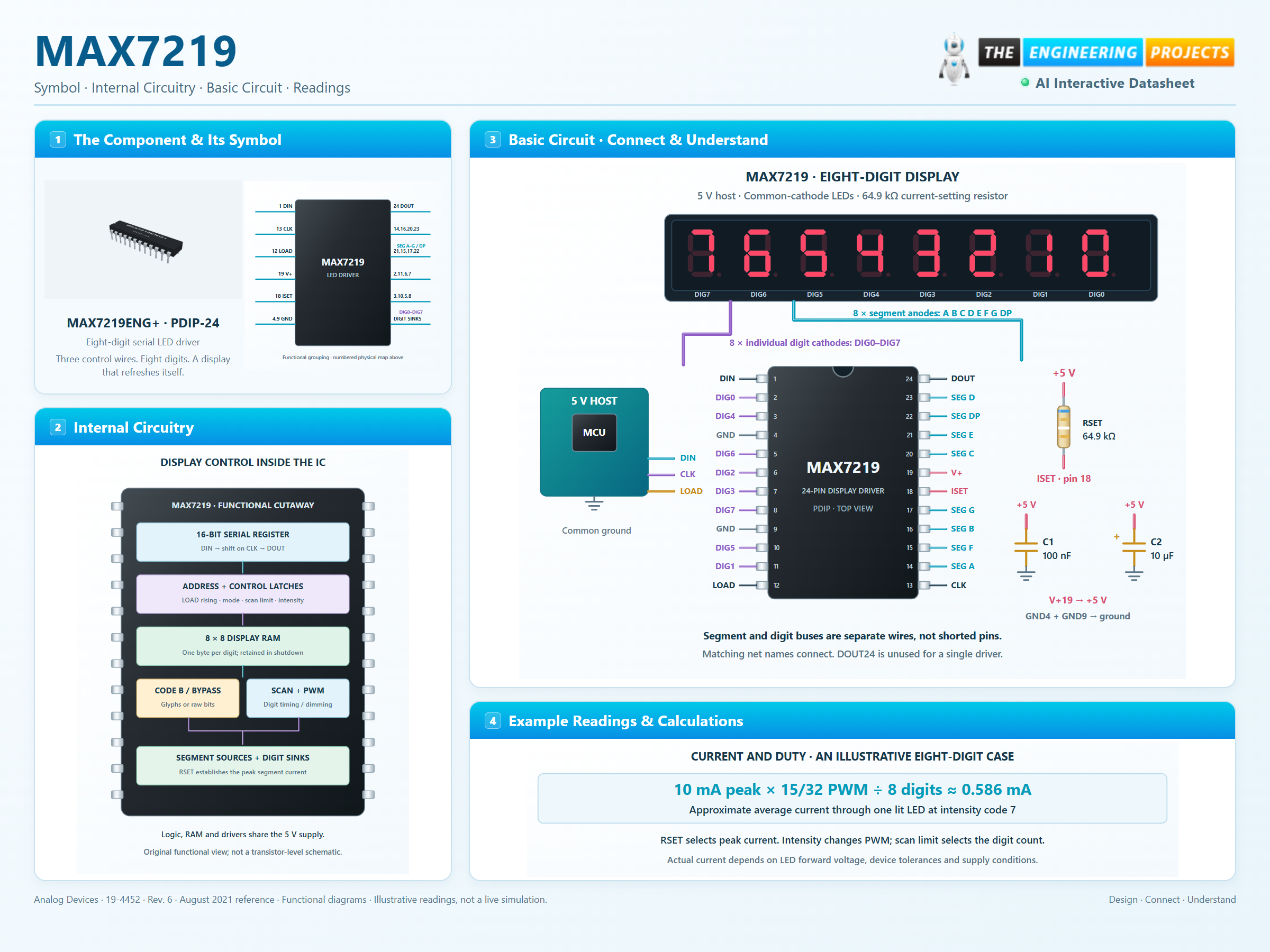
How it works
3 stages · Explore one step at a time
Wire the display by function
Segment anodes share A–G/DP buses; each digit has its own common cathode.
Load bytes through DIN and CLK
Send address then data, MSB first, and latch with LOAD rising.
Scan and dim in hardware
RAM preserves the pattern while internal scanning and PWM drive the LEDs.
Step 1 of 3
MAX7219 in a circuit
Physical IC, named segment buses and separate digit returns.
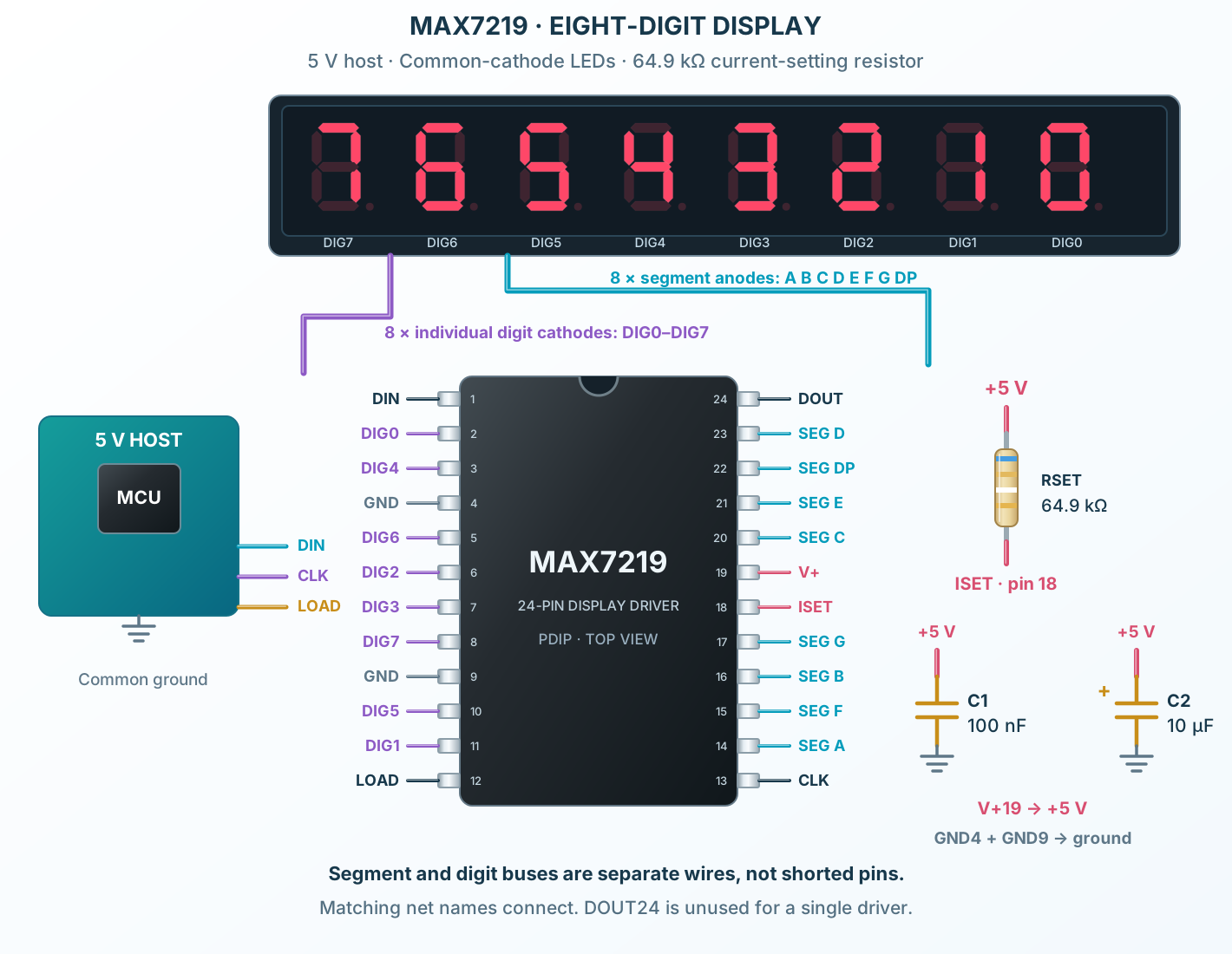
Connect it, step by step
Follow the component values and pin connections
Power and bypass
Use both ground pins and place 100 nF plus 10 µF close to V+.
Connect the digit and segment buses
Use common-cathode displays and map each output by its name.
Configure then enable
Initialize mode, scan limit, RAM and brightness before leaving shutdown.
Inside MAX7219
Serial storage, scan control and current drivers inside the IC.
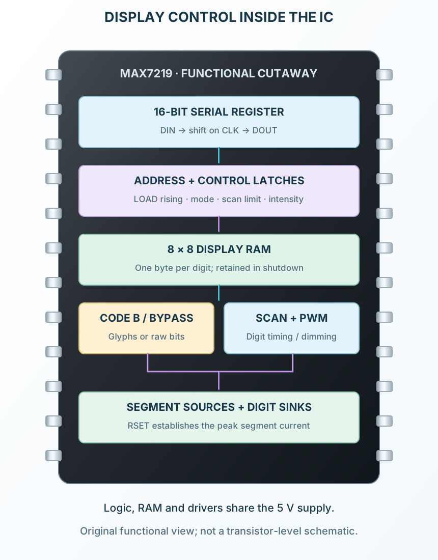
Explore the circuit
Select a stage to see its role and connections
Receive and latch
CLK shifts the command; LOAD selects the destination register.
Store and decode
Each digit has a RAM byte; Code B can be enabled individually.
Drive the display
RSET controls peak segment current; scanning selects digit cathodes.
Selected packagePDIP-24MAX7219ENG+
Physical connections24 pinsPackage-specific numbering
Reference collection7 tables45 parameters & pin functions
Pin reference
Signal names, electrical functions and connection guidance
Physical pin numbers24 pins
Scroll within the table to see all columns and rows.
| Pin | Signal | Type | Function & connection |
|---|---|---|---|
| DIN | Input | Accepts serial data on each rising CLK edge.Connection guidanceConnect to a 5 V host MOSI output. A guaranteed HIGH requires at least 3.5 V; use level translation with a 3.3 V host. | |
| DIG0 | Current sink | Selects digit 0 by sinking its common-cathode current.Connection guidanceConnect to the common cathode of display digit 0. Inactive digit outputs are driven HIGH on MAX7219, not high impedance. | |
| DIG4 | Current sink | Selects digit 4 by sinking its common-cathode current.Connection guidanceConnect to the common cathode of display digit 4. Inactive digit outputs are driven HIGH on MAX7219, not high impedance. | |
| GND | Ground | Supply and LED-current return.Connection guidanceConnect both ground pins to the common return. | |
| DIG6 | Current sink | Selects digit 6 by sinking its common-cathode current.Connection guidanceConnect to the common cathode of display digit 6. Inactive digit outputs are driven HIGH on MAX7219, not high impedance. | |
| DIG2 | Current sink | Selects digit 2 by sinking its common-cathode current.Connection guidanceConnect to the common cathode of display digit 2. Inactive digit outputs are driven HIGH on MAX7219, not high impedance. | |
| DIG3 | Current sink | Selects digit 3 by sinking its common-cathode current.Connection guidanceConnect to the common cathode of display digit 3. Inactive digit outputs are driven HIGH on MAX7219, not high impedance. | |
| DIG7 | Current sink | Selects digit 7 by sinking its common-cathode current.Connection guidanceConnect to the common cathode of display digit 7. Inactive digit outputs are driven HIGH on MAX7219, not high impedance. | |
| GND | Ground | Supply and LED-current return.Connection guidanceConnect both ground pins to the common return. | |
| DIG5 | Current sink | Selects digit 5 by sinking its common-cathode current.Connection guidanceConnect to the common cathode of display digit 5. Inactive digit outputs are driven HIGH on MAX7219, not high impedance. | |
| DIG1 | Current sink | Selects digit 1 by sinking its common-cathode current.Connection guidanceConnect to the common cathode of display digit 1. Inactive digit outputs are driven HIGH on MAX7219, not high impedance. | |
| LOAD | Input | A rising edge transfers the last 16 serial bits to the selected register.Connection guidanceHold LOW during each 16-bit transfer, then pulse HIGH. CLK still shifts the MAX7219 while LOAD is HIGH; this differs from MAX7221 chip-select behavior. | |
| CLK | Input | Serial clock: DIN shifts on rising edges and DOUT changes after falling edges.Connection guidanceConnect to host clock; maximum serial clock is 10 MHz. | |
| SEG A | Current source | Supplies the A segment anodes.Connection guidanceJoin the A anodes across all eight common-cathode digits. Peak current is set by RSET; digit multiplexing and intensity PWM determine average current. | |
| SEG F | Current source | Supplies the F segment anodes.Connection guidanceJoin the F anodes across all eight common-cathode digits. Peak current is set by RSET; digit multiplexing and intensity PWM determine average current. | |
| SEG B | Current source | Supplies the B segment anodes.Connection guidanceJoin the B anodes across all eight common-cathode digits. Peak current is set by RSET; digit multiplexing and intensity PWM determine average current. | |
| SEG G | Current source | Supplies the G segment anodes.Connection guidanceJoin the G anodes across all eight common-cathode digits. Peak current is set by RSET; digit multiplexing and intensity PWM determine average current. | |
| ISET | Analog reference | Sets the peak segment current through an external resistor.Connection guidanceConnect RSET to V+; the example uses 64.9 kΩ for a low-current red display. Choose RSET from the manufacturer table using LED forward voltage; do not leave it unconnected. | |
| V+ | Supply | Powers the serial logic, memory and display drivers.Connection guidanceUse 5 V with 100 nF ceramic and 10 µF bulk bypass near the IC. Operating supply range: 4.0–5.5 V. | |
| SEG C | Current source | Supplies the C segment anodes.Connection guidanceJoin the C anodes across all eight common-cathode digits. Peak current is set by RSET; digit multiplexing and intensity PWM determine average current. | |
| SEG E | Current source | Supplies the E segment anodes.Connection guidanceJoin the E anodes across all eight common-cathode digits. Peak current is set by RSET; digit multiplexing and intensity PWM determine average current. | |
| SEG DP | Current source | Supplies the decimal point segment anodes.Connection guidanceJoin the DP anodes across all eight common-cathode digits. Peak current is set by RSET; digit multiplexing and intensity PWM determine average current. | |
| SEG D | Current source | Supplies the D segment anodes.Connection guidanceJoin the D anodes across all eight common-cathode digits. Peak current is set by RSET; digit multiplexing and intensity PWM determine average current. | |
| DOUT | Output | Serial data output for daisy-chaining another driver.Connection guidanceConnect to the next DIN, or leave open for one IC. Never high impedance; do not connect directly to a shared MISO bus. |
No pins match these filters. Try another signal name or reset the filters.
Supply and logic levels
Recommended operating conditions
Manufacturer-referenced values7 parameters
Scroll within the table to see all columns and rows.
| Parameter | Value | Conditions / notes |
|---|---|---|
| V+ operating range | 4.0–5.5 V | Example uses regulated 5 V |
| Input HIGH / LOW | ≥3.5 V / ≤0.8 V | DIN, CLK and LOAD; 3.3 V is not a guaranteed HIGH |
| Shutdown current | 150 µA typical | 25°C, logic inputs at a supply rail |
| Display refresh | 800 Hz typical at eight digits | 500–1300 Hz specified scan range |
| Selected E temperature grade | −40 to +85°C | C grade is 0–70°C |
| Bypass capacitors | 100 nF ceramic + 10 µF bulk | Close to V+19 and ground |
| Ground contacts | Pins 4 and 9 | Connect both; carry multiplexed display return current |
No specifications match. Try a parameter name or a unit.
Check power dissipation separately from the temperature grade.
Registers and command words
16 bits, MSB first: address byte then data byte
Manufacturer-referenced values8 parameters
Scroll within the table to see all columns and rows.
| Parameter | Value | Conditions / notes |
|---|---|---|
| 0x00 · No-op | Data ignored | Use to pass a command through a daisy chain |
| 0x01–0x08 · Digits | One display byte each | Addresses correspond to DIG0–DIG7 |
| 0x09 · Decode mode | One bit per digit | 1 enables Code B; 0 selects raw segments |
| 0x0A · Intensity | Low nibble 0x0–0xF | 16 PWM settings |
| 0x0B · Scan limit | 0–7 | Selects one through eight scanned digits |
| 0x0C · Shutdown | 0=blank / 1=normal | RAM and control contents retained |
| 0x0F · Display test | 0=normal / 1=all LEDs | Overrides shutdown and intensity; disable after testing |
| Unused command bits | D15–D12 ignored | D11–D8 address; D7–D0 data |
No specifications match. Try a parameter name or a unit.
MAX7219 has no readback register command. DOUT is the serial shift output.
Decode and segment mapping
Digit data is interpreted by the decode mask
Manufacturer-referenced values7 parameters
Scroll within the table to see all columns and rows.
| Parameter | Value | Conditions / notes |
|---|---|---|
| Raw D7…D0 | DP, A, B, C, D, E, F, G | A set bit lights its segment during that digit slot |
| Code-B values 0x0–0x9 | Numerals 0–9 | Lower nibble selects the glyph |
| Code-B 0xA…0xF | −, E, H, L, P, blank | D4–D6 ignored |
| Decimal point | D7=1 | Independent of Code-B decoding |
| Raw numeral 8 | 0x7F | All seven bars on; decimal point off |
| Raw blank | 0x00 | All segments off |
| Decoded blank | 0x0F | Use only on Code-B-enabled digits |
No specifications match. Try a parameter name or a unit.
A raw matrix image needs decode mode 0x00.
Current, PWM and heat
Do not confuse peak and average LED current
Manufacturer-referenced values8 parameters
Scroll within the table to see all columns and rows.
| Parameter | Value | Conditions / notes |
|---|---|---|
| Eight-digit example RSET | 64.9 kΩ | Near the 63.7 kΩ manufacturer-table value for 10 mA at 2.0 V LED drop |
| Maximum recommended peak | 40 mA per segment | Check LED pulse rating and IC power budget |
| Minimum RSET | 9.53 kΩ | Actual current also depends on LED forward voltage |
| Intensity code k | PWM duty = (2k+1)/32 | k=0…15; applies during each digit slot |
| Per-LED average at eight digits | Approximately Ipeak × PWM duty / 8 | Multiplexing is in addition to intensity PWM |
| One / two / three digits | Peak ≤10 / 20 / 30 mA | Manufacturer limits individual digit-driver dissipation |
| Package thermal resistance | PDIP: 75°C/W; SOIC: 85°C/W | Datasheet reference values; board and cooling matter |
| Current example | 10 mA × 15/32 ÷ 8 ≈0.586 mA | Intensity code 7; approximate average per lit LED |
No specifications match. Try a parameter name or a unit.
Use scan limit for the real display topology; use intensity to dim.
Serial timing and cascading
LOAD is a latch strobe on MAX7219
Manufacturer-referenced values7 parameters
Scroll within the table to see all columns and rows.
| Parameter | Value | Conditions / notes |
|---|---|---|
| Serial clock maximum | 10 MHz | At least 50 ns HIGH and 50 ns LOW |
| DIN setup / hold | 25 ns / 0 ns | Relative to CLK rising |
| LOAD HIGH pulse | At least 50 ns | Latch after the last bit |
| LOAD rise to next CLK rise | At least 50 ns | MAX7219 requirement |
| DOUT progression | 16.5 clock cycles behind DIN | Updates on falling CLK edges; always driven |
| Chain connection | DOUT → next DIN | Share CLK and LOAD; send farthest-device word first |
| MAX7221 distinction | CS gates clocking; outputs slew-limited | Do not assume those behaviors for MAX7219 |
No specifications match. Try a parameter name or a unit.
Use a defined idle clock and latch only after a complete transfer.
Eight-digit startup example
Example values for decoded numbers
Manufacturer-referenced values8 parameters
Scroll within the table to see all columns and rows.
| Parameter | Value | Conditions / notes |
|---|---|---|
| Blank during setup | 0x0C, 0x00 | Shutdown while configuring |
| Disable test | 0x0F, 0x00 | Avoid the all-on override |
| Enable Code B | 0x09, 0xFF | All eight digits decoded |
| Select eight digits | 0x0B, 0x07 | DIG0 through DIG7 |
| Set moderate PWM | 0x0A, 0x07 | 15/32 slot duty |
| Initialize display RAM | 0x01…0x08 with 0x0F | Blank every decoded digit |
| Write a zero on DIG0 | 0x01, 0x00 | Use 0x80 to include its decimal point |
| Enable display | 0x0C, 0x01 | Normal scanning begins |
No specifications match. Try a parameter name or a unit.
Commands are two bytes each, followed by LOAD rising.
No matching rowsTry a pin name, parameter, unit or test condition, or reset the filters.
Numeric instrument panels
Display measurements and decimal points while the host performs acquisition.
Manufacturer application guideEight-by-eight LED matrices
Disable Code B and write raw segment bytes to form patterns.
Manufacturer application guideLonger cascaded displays
Chain serial outputs and send no-op words to devices that should retain their registers.
Manufacturer application guideTake it into ProTech
Find MAX7219 in the Components Library to place its schematic symbol and connect its pins.
Reference page · circuit simulation model not yet availableOpen ProTech