MCP2562High-speed CAN transceiver with VIO
Connect low-voltage controller logic to a 5 V CAN physical layer.
MCP2562 translates the logic signals from a CAN controller into the differential CANH and CANL signals on the cable. It provides the physical interface, while a separate controller handles frames, identifiers, arbitration and error accounting. The device supports classical high-speed CAN operation up to 1 Mbit/s. Its bus circuitry uses a 5 V supply, while the separate VIO pin supports controller I/O supplies from 1.8 V to 5.5 V. This allows a 3.3 V controller to use the transceiver without placing 5 V logic on its receive input. Both supply domains need local bypassing and a shared reference. The example uses 5 V at VDD, 3.3 V at VIO and STBY held LOW. Two 120 Ω end terminators give a nominal 60 Ω differential load. Normal CAN traffic contains dominant and recessive bits; the built-in timeout deliberately prevents a transmitter from holding the bus dominant indefinitely.
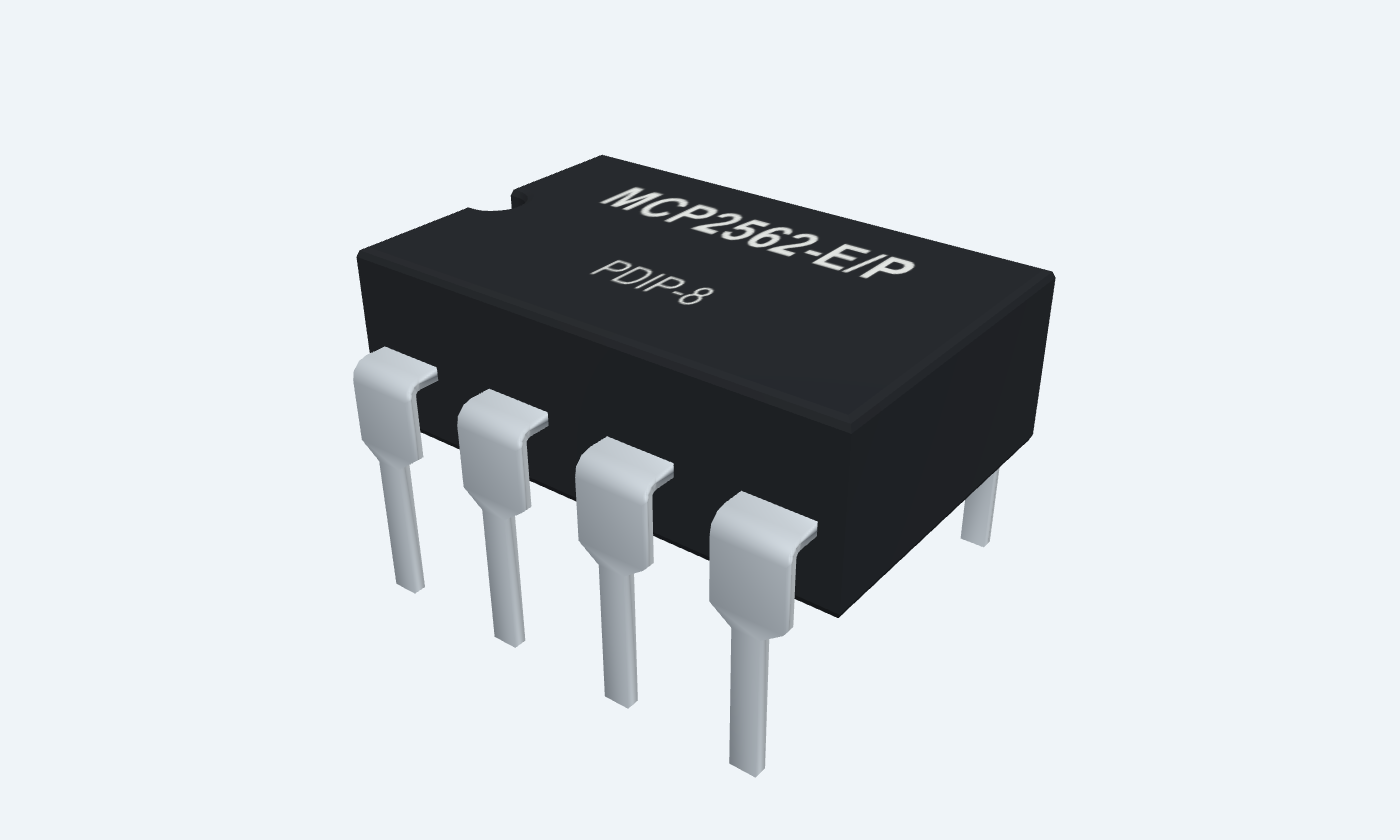
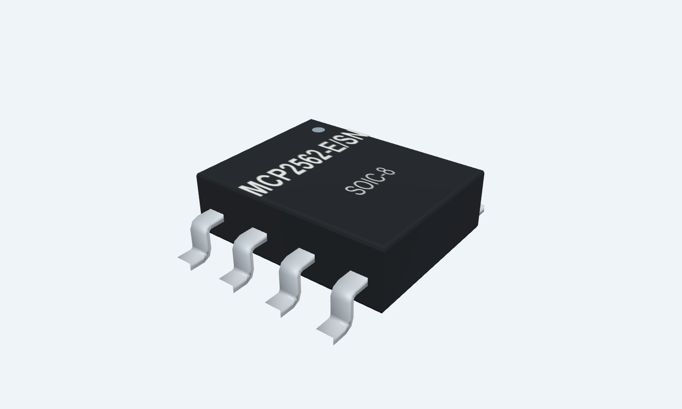

8Physical pins
MCP2562-E/PPDIP-8
Manufacturer-referencedMicrochip Technology
Pin diagram
Select a pin to explore its connection
Highlight
MCP2562PDIP-8Top view
MCP2562SOIC-8Top view
Click a lead or use the arrow keys. Top view
PIN 1 · CAN controller interface
Transmit data inputTXD
Function
LOW requests a dominant bus state; HIGH releases the bus to recessive unless another node is dominant.
How to connect
Connect to the CAN controller TX output.
Electrical note
Internal pull-up to VIO; prolonged LOW invokes dominant timeout.
PIN 2 · Ground
GroundVSS
Function
Supply and logic reference.
How to connect
Join controller ground and the intended bus reference.
PIN 3 · Supply
Bus-side supplyVDD
Function
Powers the transmitter and receiver.
How to connect
Use 4.5–5.5 V; bypass locally with 100 nF to VSS.
PIN 4 · CAN controller interface
Receive data outputRXD
Function
LOW reports a dominant bus, HIGH a recessive bus in Normal mode. Standby reception is filtered.
How to connect
Connect to CAN controller RX.
Electrical note
Output HIGH level follows VIO, not the 5 V bus supply.
PIN 5 · Supply
Digital I/O supplyVIO
Function
Sets the voltage domain for TXD, RXD and STBY.
How to connect
Connect to the controller I/O supply, 1.8–5.5 V, and bypass with 100 nF.
Electrical note
This pin is VIO on MCP2562; MCP2561 has SPLIT here instead.
PIN 6 · Differential CAN pair
CAN low bus terminalCANL
Function
Low-going side of the differential bus during a dominant bit.
How to connect
Connect to CANL in the twisted pair.
PIN 7 · Differential CAN pair
CAN high bus terminalCANH
Function
High-going side of the differential bus during a dominant bit.
How to connect
Connect to CANH in the twisted pair.
PIN 8 · Operating mode
Operating-mode inputSTBY
Function
LOW selects Normal mode; HIGH selects Standby with a filtered low-power receiver.
How to connect
Hold LOW for the example, or control from a VIO-compatible GPIO.
Electrical note
Internal pull-up favors standby if left open; drive explicitly.
Key specifications
The VIO domain matches the controller logic. The 5 V domain drives and senses CANH/CANL. Protection and a standby wake-up filter surround those signal paths.
Bus supply4.5–5.5 V
I/O supply1.8–5.5 V
Maximum bit rate1 Mbit/s
Selected E grade−40–125 °C
Package details
MCP2562-E/P · PDIP-8
| Property | Details |
|---|---|
| Manufacturer | Microchip Technology |
| Part number | MCP2562-E/P |
| Package | PDIP-8 |
| Connections | 8 pins |
| Mounting | Through-hole |
| Lead pitch | 2.54 mm |
| Package code | dip |
| Thermal reference | Board and package dependent; see manufacturer data |
Logic and mode behavior
LOW / HIGH relative to VIO
Manufacturer specifications 6 parameters
Scroll sideways to see all columns.
| Parameter | Value | Conditions / notes |
|---|---|---|
| Normal, TXD LOW | Driver requests dominant | STBY LOW; RXD LOW if dominant is established |
| Normal, TXD HIGH | Driver releases to recessive | Another node may still force dominant |
| Normal, bus dominant | RXD LOW | Receiver reflects differential bus state |
| Normal, bus recessive | RXD HIGH | Receiver output is referenced to VIO |
| Standby | Driver disabled; filtered reception | STBY HIGH; LOW on RXD indicates wake-up activity |
| Unpowered / brownout | Bus driver high impedance | Observe specified supply sequencing and thresholds |
No specifications match. Try a parameter name or a unit.
The mode input has an internal pull-up. Do not leave it floating when Normal mode is intended.
Operating and logic limits
Selected E grade · −40 to +125°C
Manufacturer specifications 8 parameters
Scroll sideways to see all columns.
| Parameter | Value | Conditions / notes |
|---|---|---|
| VDD | 4.5–5.5 V | Bus transmitter and receiver supply |
| VIO | 1.8–5.5 V | TXD, RXD and STBY voltage domain |
| Input HIGH | ≥ 0.7 × VIO | TXD and STBY |
| Input LOW | ≤ 0.3 × VIO | TXD and STBY |
| RXD HIGH | ≥ VIO − 0.4 V | −1 mA output current |
| RXD LOW | ≤ 0.4 V | 4 mA output current |
| Normal VDD current | 5 mA typ. / 10 mA max. recessive | 45 mA typ. / 70 mA max. dominant; 60 Ω load |
| Standby total | 5 µA typical / 15 µA maximum | MCP2562; includes IIO |
No specifications match. Try a parameter name or a unit.
Typical values describe nominal behavior and are not guaranteed limits.
Differential voltage levels
VDD 4.5–5.5 V; stated load conditions
Manufacturer specifications 7 parameters
Scroll sideways to see all columns.
| Parameter | Value | Conditions / notes |
|---|---|---|
| CANH dominant | 3.5 V typical | 2.75–4.5 V; differential load 50–65 Ω |
| CANL dominant | 1.5 V typical | 0.5–2.25 V; differential load 50–65 Ω |
| Dominant differential output | 2.0 V typical; 1.5–3.0 V | CANH − CANL; load 50–65 Ω |
| Recessive output | VDD / 2 typical on each line | No load; differential voltage near zero |
| Normal receiver recessive | −1.0 to +0.5 V differential | Specified bus common-mode conditions |
| Normal receiver dominant | +0.9 V to VDD differential | Transition region between 0.5 and 0.9 V |
| Receiver common-mode characterization | −12 to +12 V | Production tested from −2 to +7 V; see manufacturer note |
No specifications match. Try a parameter name or a unit.
Voltage states are bus conditions, not separate logic supply levels.
Timing and protection
Electrical table conditions apply
Manufacturer specifications 7 parameters
Scroll sideways to see all columns.
| Parameter | Value | Conditions / notes |
|---|---|---|
| Bit rate | 14.4 kbit/s to 1 Mbit/s | Dominant timeout constrains very slow traffic |
| TXD LOW → bus dominant | 70 ns maximum | Propagation, specified test load |
| TXD HIGH → bus recessive | 125 ns maximum | Propagation, specified test load |
| Bus dominant → RXD LOW | 70 ns maximum | Normal mode |
| Standby wake-up filter | 1 µs typical; 0.5–4 µs | Not the Normal-mode data path |
| Dominant timeout | 1.25 ms typical | TXD must return HIGH to release transmitter lockout |
| Thermal shutdown | 175°C typical junction | Protection threshold, not a permitted operating temperature |
No specifications match. Try a parameter name or a unit.
Protection does not replace a network-specific transient, grounding or isolation design.
3.3 V controller connection
A CAN controller is required
Manufacturer specifications 7 parameters
Scroll sideways to see all columns.
| Parameter | Value | Conditions / notes |
|---|---|---|
| VDD3 | +5 V with 100 nF to GND | Keep bypass close to supply pins |
| VIO5 | +3.3 V with 100 nF to GND | Same rail as controller I/O |
| VSS2 | Common reference | Join controller ground |
| TXD1 / RXD4 | CAN_TX / CAN_RX | Use the controller’s CAN peripheral, not UART |
| STBY8 | GND in the always-on example | Use a GPIO if standby is required |
| CANH7 / CANL6 | Twisted pair to other CAN nodes | Keep topology and stubs appropriate to bit rate |
| Termination | 120 Ω at each physical cable end | Two parallel end loads are nominally 60 Ω |
No specifications match. Try a parameter name or a unit.
Another active node must share timing and acknowledge valid frames.
Packages and stress ratings
MCP2562-E/P · PDIP-8
Manufacturer specifications 7 parameters
Scroll sideways to see all columns.
| Parameter | Value | Conditions / notes |
|---|---|---|
| PDIP-8 P | 2.54 mm lead pitch | Through-hole version shown |
| SOIC-8 SN | 1.27 mm lead pitch | Narrow SMD version shown |
| Selected grade E | −40 to +125°C ambient | H grade reaches +150°C; not selected here |
| VDD / VIO absolute maximum | 7 V | Normal operation ends at 5.5 V |
| Bus pins absolute DC range | −58 to +58 V | Stress rating, not receiver operating common mode |
| Storage range | −55 to +150°C | Unpowered |
| MCP2561 difference | Pin 5 is SPLIT, not VIO | Do not substitute its wiring for MCP2562 |
No specifications match. Try a parameter name or a unit.
Use the exact ordering code and current manufacturer drawing when reviewing PCB lands.
Connections by function
Select a pin for its function, connection guidance and electrical notes.
CAN controller interface2 pins
Ground1 pin
Supply2 pins
Differential CAN pair2 pins
Operating mode1 pin
CAN controller interface2 pins
Ground1 pin
Supply2 pins
Differential CAN pair2 pins
Operating mode1 pin
MCP2562 at a glance
Follow the labeled connections and functional stages
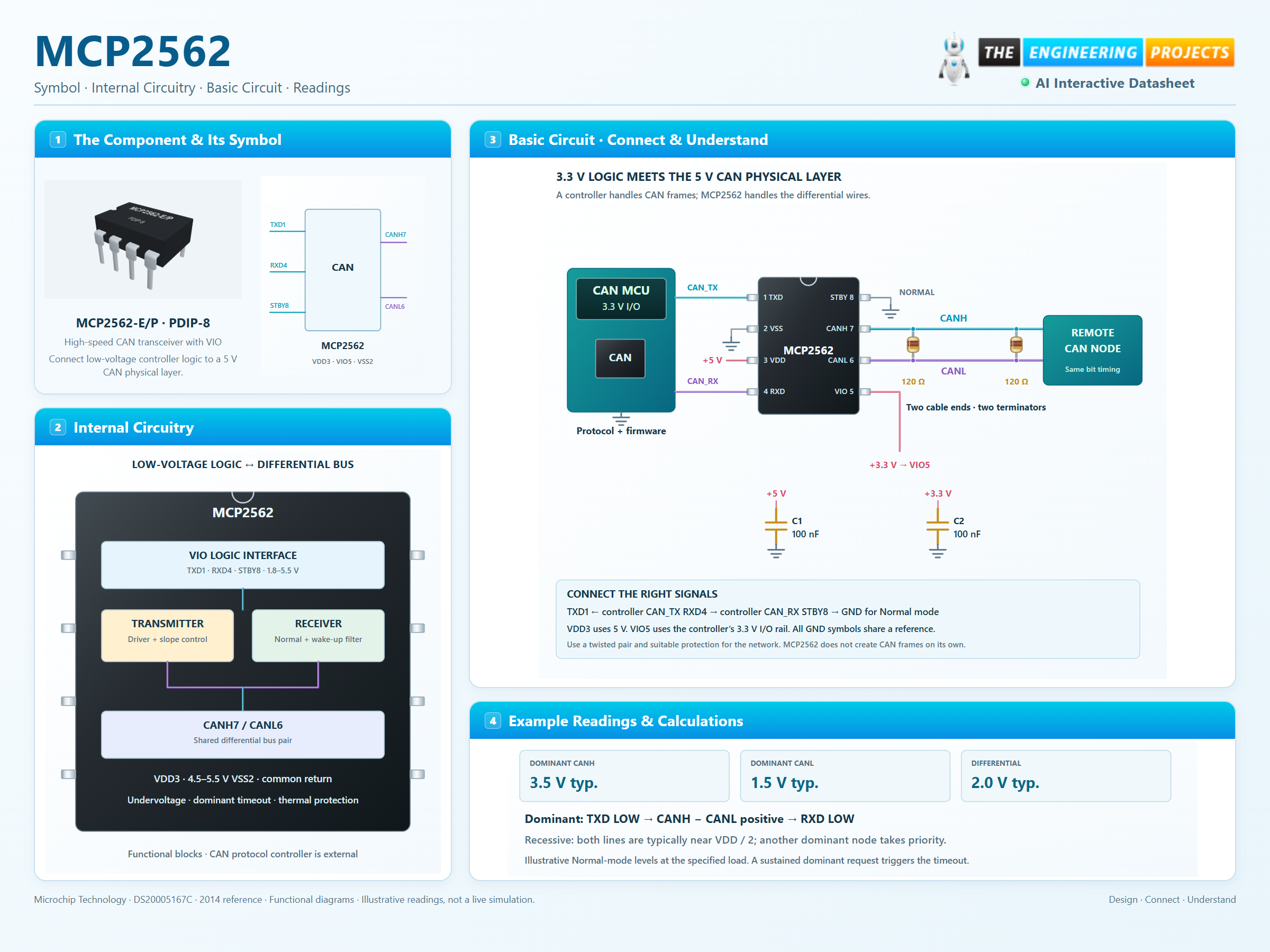
How it works
3 stages · Explore one step at a time
Match the logic supply
Connect VIO to the controller’s I/O rail and VDD to a regulated 5 V rail. Bypass both close to the device.
Transmit and monitor
TXD LOW requests dominant. The differential receiver reports the actual bus through RXD, including another node overriding recessive.
Sleep and wake deliberately
STBY HIGH stops the driver and enables filtered bus wake-up monitoring. Return STBY LOW before normal data exchange.
Step 1 of 3
MCP2562 in a circuit
5 V bus supply, 3.3 V I/O and correct cable-end termination.
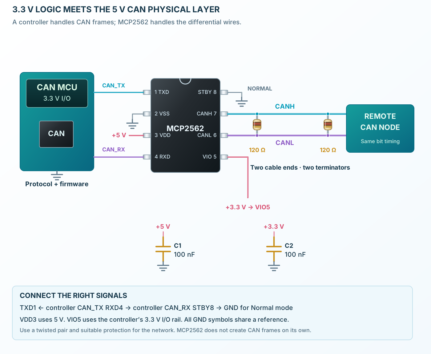
Connect it, step by step
Follow the component values and pin connections
Power both domains
Bypass VDD and VIO separately.
Connect the controller
Controller TX drives TXD; RXD feeds controller RX; both use VIO-compatible logic.
Terminate the pair
Put 120 Ω across CANH/CANL only at each cable end, not at every node.
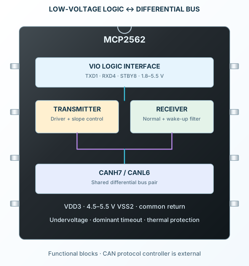
Inside MCP2562
Logic-domain translation and differential signaling in one package.
Explore the circuit
Select a stage to see its role and connections
Translate logic
VIO sets TXD, RXD and STBY levels independently of VDD.
Drive and receive
The driver and receiver share CANH and CANL.
Manage faults
Undervoltage, dominant timeout and thermal protection manage specified fault conditions.
Selected packagePDIP-8MCP2562-E/P
Physical connections8 pinsPackage-specific numbering
Reference collection7 tables42 parameters & pin functions
Pin reference
Signal names, electrical functions and connection guidance
Physical pin numbers8 pins
Scroll within the table to see all columns and rows.
| Pin | Signal | Type | Function & connection |
|---|---|---|---|
| TXD | Transmit data input | LOW requests a dominant bus state; HIGH releases the bus to recessive unless another node is dominant.Connection guidanceConnect to the CAN controller TX output. Internal pull-up to VIO; prolonged LOW invokes dominant timeout. | |
| VSS | Ground | Supply and logic reference.Connection guidanceJoin controller ground and the intended bus reference. | |
| VDD | Bus-side supply | Powers the transmitter and receiver.Connection guidanceUse 4.5–5.5 V; bypass locally with 100 nF to VSS. | |
| RXD | Receive data output | LOW reports a dominant bus, HIGH a recessive bus in Normal mode. Standby reception is filtered.Connection guidanceConnect to CAN controller RX. Output HIGH level follows VIO, not the 5 V bus supply. | |
| VIO | Digital I/O supply | Sets the voltage domain for TXD, RXD and STBY.Connection guidanceConnect to the controller I/O supply, 1.8–5.5 V, and bypass with 100 nF. This pin is VIO on MCP2562; MCP2561 has SPLIT here instead. | |
| CANL | CAN low bus terminal | Low-going side of the differential bus during a dominant bit.Connection guidanceConnect to CANL in the twisted pair. | |
| CANH | CAN high bus terminal | High-going side of the differential bus during a dominant bit.Connection guidanceConnect to CANH in the twisted pair. | |
| STBY | Operating-mode input | LOW selects Normal mode; HIGH selects Standby with a filtered low-power receiver.Connection guidanceHold LOW for the example, or control from a VIO-compatible GPIO. Internal pull-up favors standby if left open; drive explicitly. |
No pins match these filters. Try another signal name or reset the filters.
Logic and mode behavior
LOW / HIGH relative to VIO
Manufacturer-referenced values6 parameters
Scroll within the table to see all columns and rows.
| Parameter | Value | Conditions / notes |
|---|---|---|
| Normal, TXD LOW | Driver requests dominant | STBY LOW; RXD LOW if dominant is established |
| Normal, TXD HIGH | Driver releases to recessive | Another node may still force dominant |
| Normal, bus dominant | RXD LOW | Receiver reflects differential bus state |
| Normal, bus recessive | RXD HIGH | Receiver output is referenced to VIO |
| Standby | Driver disabled; filtered reception | STBY HIGH; LOW on RXD indicates wake-up activity |
| Unpowered / brownout | Bus driver high impedance | Observe specified supply sequencing and thresholds |
No specifications match. Try a parameter name or a unit.
The mode input has an internal pull-up. Do not leave it floating when Normal mode is intended.
Operating and logic limits
Selected E grade · −40 to +125°C
Manufacturer-referenced values8 parameters
Scroll within the table to see all columns and rows.
| Parameter | Value | Conditions / notes |
|---|---|---|
| VDD | 4.5–5.5 V | Bus transmitter and receiver supply |
| VIO | 1.8–5.5 V | TXD, RXD and STBY voltage domain |
| Input HIGH | ≥ 0.7 × VIO | TXD and STBY |
| Input LOW | ≤ 0.3 × VIO | TXD and STBY |
| RXD HIGH | ≥ VIO − 0.4 V | −1 mA output current |
| RXD LOW | ≤ 0.4 V | 4 mA output current |
| Normal VDD current | 5 mA typ. / 10 mA max. recessive | 45 mA typ. / 70 mA max. dominant; 60 Ω load |
| Standby total | 5 µA typical / 15 µA maximum | MCP2562; includes IIO |
No specifications match. Try a parameter name or a unit.
Typical values describe nominal behavior and are not guaranteed limits.
Differential voltage levels
VDD 4.5–5.5 V; stated load conditions
Manufacturer-referenced values7 parameters
Scroll within the table to see all columns and rows.
| Parameter | Value | Conditions / notes |
|---|---|---|
| CANH dominant | 3.5 V typical | 2.75–4.5 V; differential load 50–65 Ω |
| CANL dominant | 1.5 V typical | 0.5–2.25 V; differential load 50–65 Ω |
| Dominant differential output | 2.0 V typical; 1.5–3.0 V | CANH − CANL; load 50–65 Ω |
| Recessive output | VDD / 2 typical on each line | No load; differential voltage near zero |
| Normal receiver recessive | −1.0 to +0.5 V differential | Specified bus common-mode conditions |
| Normal receiver dominant | +0.9 V to VDD differential | Transition region between 0.5 and 0.9 V |
| Receiver common-mode characterization | −12 to +12 V | Production tested from −2 to +7 V; see manufacturer note |
No specifications match. Try a parameter name or a unit.
Voltage states are bus conditions, not separate logic supply levels.
Timing and protection
Electrical table conditions apply
Manufacturer-referenced values7 parameters
Scroll within the table to see all columns and rows.
| Parameter | Value | Conditions / notes |
|---|---|---|
| Bit rate | 14.4 kbit/s to 1 Mbit/s | Dominant timeout constrains very slow traffic |
| TXD LOW → bus dominant | 70 ns maximum | Propagation, specified test load |
| TXD HIGH → bus recessive | 125 ns maximum | Propagation, specified test load |
| Bus dominant → RXD LOW | 70 ns maximum | Normal mode |
| Standby wake-up filter | 1 µs typical; 0.5–4 µs | Not the Normal-mode data path |
| Dominant timeout | 1.25 ms typical | TXD must return HIGH to release transmitter lockout |
| Thermal shutdown | 175°C typical junction | Protection threshold, not a permitted operating temperature |
No specifications match. Try a parameter name or a unit.
Protection does not replace a network-specific transient, grounding or isolation design.
3.3 V controller connection
A CAN controller is required
Manufacturer-referenced values7 parameters
Scroll within the table to see all columns and rows.
| Parameter | Value | Conditions / notes |
|---|---|---|
| VDD3 | +5 V with 100 nF to GND | Keep bypass close to supply pins |
| VIO5 | +3.3 V with 100 nF to GND | Same rail as controller I/O |
| VSS2 | Common reference | Join controller ground |
| TXD1 / RXD4 | CAN_TX / CAN_RX | Use the controller’s CAN peripheral, not UART |
| STBY8 | GND in the always-on example | Use a GPIO if standby is required |
| CANH7 / CANL6 | Twisted pair to other CAN nodes | Keep topology and stubs appropriate to bit rate |
| Termination | 120 Ω at each physical cable end | Two parallel end loads are nominally 60 Ω |
No specifications match. Try a parameter name or a unit.
Another active node must share timing and acknowledge valid frames.
Packages and stress ratings
MCP2562-E/P · PDIP-8
Manufacturer-referenced values7 parameters
Scroll within the table to see all columns and rows.
| Parameter | Value | Conditions / notes |
|---|---|---|
| PDIP-8 P | 2.54 mm lead pitch | Through-hole version shown |
| SOIC-8 SN | 1.27 mm lead pitch | Narrow SMD version shown |
| Selected grade E | −40 to +125°C ambient | H grade reaches +150°C; not selected here |
| VDD / VIO absolute maximum | 7 V | Normal operation ends at 5.5 V |
| Bus pins absolute DC range | −58 to +58 V | Stress rating, not receiver operating common mode |
| Storage range | −55 to +150°C | Unpowered |
| MCP2561 difference | Pin 5 is SPLIT, not VIO | Do not substitute its wiring for MCP2562 |
No specifications match. Try a parameter name or a unit.
Use the exact ordering code and current manufacturer drawing when reviewing PCB lands.
No matching rowsTry a pin name, parameter, unit or test condition, or reset the filters.
Low-voltage CAN nodes
Interface 1.8 V or 3.3 V controller logic with a 5 V CAN transceiver.
Manufacturer application guideDistributed control
Connect control modules over a correctly terminated high-speed CAN network.
Manufacturer application guideStandby-aware equipment
Use filtered bus activity to wake a controller before returning to Normal mode.
Manufacturer application guideTake it into ProTech
Find MCP2562 in the Components Library to place its schematic symbol and connect its pins.
Reference page · circuit simulation model not yet availableOpen ProTech