Real View
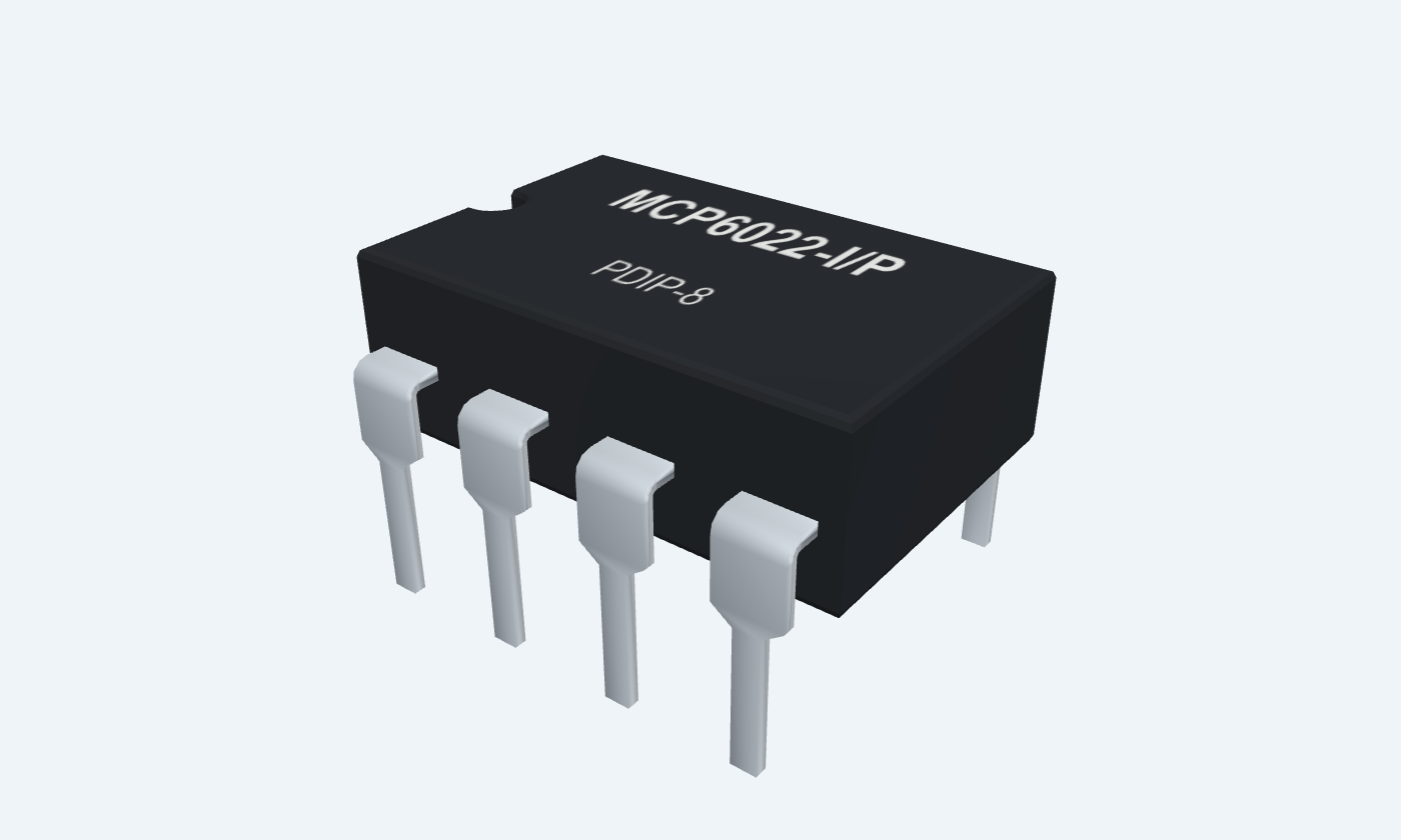
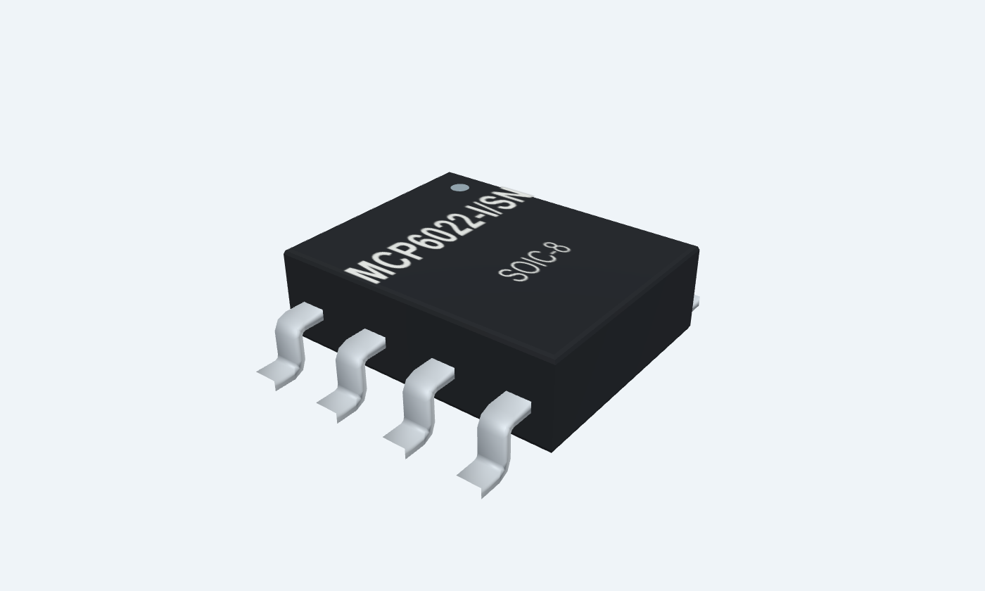
Two fast analog channels from a single low-voltage supply.
MCP6022 integrates two CMOS operational amplifiers with rail-to-rail inputs and outputs. Both channels share a 2.5–5.5 V supply, but each has independent signal inputs, feedback and output. The typical gain-bandwidth product is 10 MHz. The example uses a 5 V supply and a common 0.50 V DC input. Channel A has a gain of three and channel B is a voltage follower, producing ideal outputs of 1.50 V and 0.50 V. Local 100 nF bypass and nearby 1 µF bulk storage help keep the supply quiet. This page follows the industrial MCP6022-I/P and MCP6022-I/SN parts, specified from −40 to +85°C. It is the dual amplifier: the reference-voltage output and chip-select feature of certain single-amplifier family members do not exist on MCP6022.
Select a pin to explore its connection
Click a lead or use the arrow keys. Top view
Channel A output.
Return to IN1− through 20 kΩ; connect a high-impedance meter.
Channel A negative-feedback node.
Join 20 kΩ from OUT1 and 10 kΩ to signal ground.
Channel A signal input.
Apply VIN = 0.50 V relative to ground.
Supply return shared by both amplifiers.
Connect directly to common ground.
Channel B signal input.
Connect to the same VIN in the illustrated follower.
Channel B feedback input.
Connect directly to OUT2 pin 7.
Channel B output.
Connect to IN2−; leave unloaded or use a high-impedance instrument.
Positive rail shared by both amplifiers.
Connect +5 V; bypass to ground with 100 nF close to pins 8 and 4.
Use independent feedback for each channel, common supply decoupling and clean high-impedance nodes. Allow for source and output loading even in a rail-to-rail circuit.
MCP6022-I/P · PDIP-8
| Property | Details |
|---|---|
| Manufacturer | Microchip Technology |
| Part number | MCP6022-I/P |
| Package | PDIP-8 |
| Connections | 8 pins |
| Mounting | Through-hole |
| Lead pitch | 2.54 mm |
| Package code | PDIP-8 |
| Thermal reference | See operating and package limits |
MCP6022-I/P and MCP6022-I/SN
Scroll sideways to see all columns.
| Parameter | Value | Conditions / notes |
|---|---|---|
| Supply span | 2.5–5.5 V | VDD minus VSS |
| Industrial ambient range | −40 to +85°C | Selected I-grade parts |
| Input common-mode interval | VSS − 0.3 V to VDD + 0.3 V | Input voltage and current protection limits still apply |
| Example rails | VDD8 = 5 V; VSS4 = 0 V | Supply return is also signal ground |
| Typical current per amplifier | 1.0 mA | 0.5 mA minimum; 1.35 mA maximum, unloaded at 25°C |
| Nominal two-channel current | 2.0 mA | Before external load current |
| No VREF or chip-select pin | MCP6022 has two amplifiers | Do not apply MCP6021/6023 single-amplifier pin functions |
No specifications match. Try a parameter name or a unit.
Unless stated otherwise, electrical values follow the manufacturer 25°C, 2.5–5.5 V, midsupply signal and 10 kΩ-to-midsupply test conditions.
Industrial grade · 25°C unless stated
Scroll sideways to see all columns.
| Parameter | Value | Conditions / notes |
|---|---|---|
| Input offset voltage | ±500 µV maximum | VCM = 0 V; selected industrial grade |
| Typical offset drift | ±3.5 µV/°C | Characterized over −40 to +125°C |
| Input bias current | 1 pA typical | Room temperature |
| Bias current at +85°C | 30 pA typical; 150 pA maximum | Industrial temperature parts |
| Input offset current | ±1 pA typical | Room temperature |
| CMRR over full common-mode range | 74 dB minimum; 90 dB typical | VDD = 5 V; VCM = −0.3 to 5.3 V |
| Supply rejection | 74 dB minimum; 90 dB typical | VCM = 0 V |
| Open-loop gain | 90 dB minimum; 110 dB typical | VCM = 0; VOUT = VSS + 0.3 to VDD − 0.3 V |
| Output swing endpoints | VSS + 15 mV to VDD − 20 mV | 10 kΩ to midsupply; 0.5 V differential overdrive |
No specifications match. Try a parameter name or a unit.
The swing test uses input overdrive; do not treat its endpoints as precision closed-loop headroom at arbitrary load.
Typical values at manufacturer AC conditions
Scroll sideways to see all columns.
| Parameter | Value | Conditions / notes |
|---|---|---|
| Gain-bandwidth product | 10 MHz | Closed-loop bandwidth depends on noise gain |
| Slew rate | 7.0 V/µs | Large-signal slope limit |
| Phase margin | 65° | Gain +1; CL = 60 pF |
| Settling to 0.2% | 250 ns | Gain +1; 100 mV peak-to-peak output |
| Voltage-noise density | 8.7 nV/√Hz | 10 kHz |
| Integrated low-frequency noise | 2.9 µV peak-to-peak | 0.1–10 Hz |
| Current-noise density | 3 fA/√Hz | 1 kHz |
| THD + noise | 0.00053% | 1 kHz; gain +1; VDD 5 V; output 0.25–3.25 V; 22 kHz bandwidth |
No specifications match. Try a parameter name or a unit.
Small-signal bandwidth, large-signal slew and settling describe different limitations.
A fast CMOS amplifier needs short loops
Scroll sideways to see all columns.
| Parameter | Value | Conditions / notes |
|---|---|---|
| Local bypass | 100 nF in the example | Manufacturer recommends 10–100 nF within 2 mm of VDD |
| Nearby bulk storage | 1 µF or larger | Within 100 mm; may be shared by nearby analog parts |
| Feedback network | Short routes around each input/output pair | The 20 kΩ / 10 kΩ example is a low-frequency demonstration |
| Parasitic capacitance | Check feedback resistance against input and board capacitance | High-frequency noise gain can rise and phase margin can fall |
| Capacitive loads | Choose an isolation network for the actual load | Do not assume stable direct drive of long cables |
| Input leakage | Clean high-impedance nodes | Temperature, moisture and contamination increase errors |
| Unused channel | Stable negative feedback to a valid reference | Do not leave its inputs floating |
No specifications match. Try a parameter name or a unit.
Use the manufacturer capacitive-load and feedback-capacitance guidance for high-frequency designs.
Absolute ratings are not normal operating targets
Scroll sideways to see all columns.
| Parameter | Value | Conditions / notes |
|---|---|---|
| Absolute supply | 7.0 V | Normal operating upper limit is 5.5 V |
| Analog-input current | ±2 mA absolute maximum | Provide the specified protection if inputs can exceed safe voltage limits |
| Output / supply-pin current | ±30 mA absolute maximum | Not a recommended continuous load current |
| Junction / storage | 150°C maximum / −65 to +150°C | Do not substitute these for ambient operating limits |
| Extended E-grade offset | ±250 µV at 25°C, VDD 5 V, VCM 0 V | A different grade; not used as the I-grade limit here |
| Extended E-grade ambient | −40 to +125°C | The selected I-grade page uses −40 to +85°C |
No specifications match. Try a parameter name or a unit.
Power dissipation and board thermal conditions can constrain usable current before an absolute limit is reached.
5 V single supply · common ground
Scroll sideways to see all columns.
| Parameter | Value | Conditions / notes |
|---|---|---|
| Input VIN | 0.50 V | Pins 3 and 5; common signal ground |
| Channel A feedback | 20 kΩ | OUT1 pin 1 to IN1− pin 2 |
| Channel A ground resistor | 10 kΩ | IN1− pin 2 to 0 V |
| Channel A ideal output | 1.50 V | 0.50 × (1 + 20 / 10) |
| Channel B feedback | Direct connection | OUT2 pin 7 to IN2− pin 6 |
| Channel B ideal output | 0.50 V | Unity-gain follower |
| Bypass capacitors | 100 nF | VDD pin 8 to ground pin 4 |
| Bulk bypass | 1 µF minimum | Nearby between +5 V and GND; may be shared |
No specifications match. Try a parameter name or a unit.
The supply return and signal ground are common. Keep the bypass loop short.
MCP6022-I/P · PDIP-8
Scroll sideways to see all columns.
| Parameter | Value | Conditions / notes |
|---|---|---|
| Lead pitch | 2.54 mm | Through-hole |
| Channel A | OUT1 1; IN1− 2; IN1+ 3 | Independent feedback loop |
| Channel B | IN2+ 5; IN2− 6; OUT2 7 | Independent feedback loop |
| Supply | VSS 4; VDD 8 | Shared by both channels |
| Package orientation | Top view; pin 1 at the marker | Counterclockwise numbering |
No specifications match. Try a parameter name or a unit.
This dual-amplifier pinout differs from single amplifiers such as TL081 or LM741.
Select a pin for its function, connection guidance and electrical notes.
Follow the labeled connections and functional stages
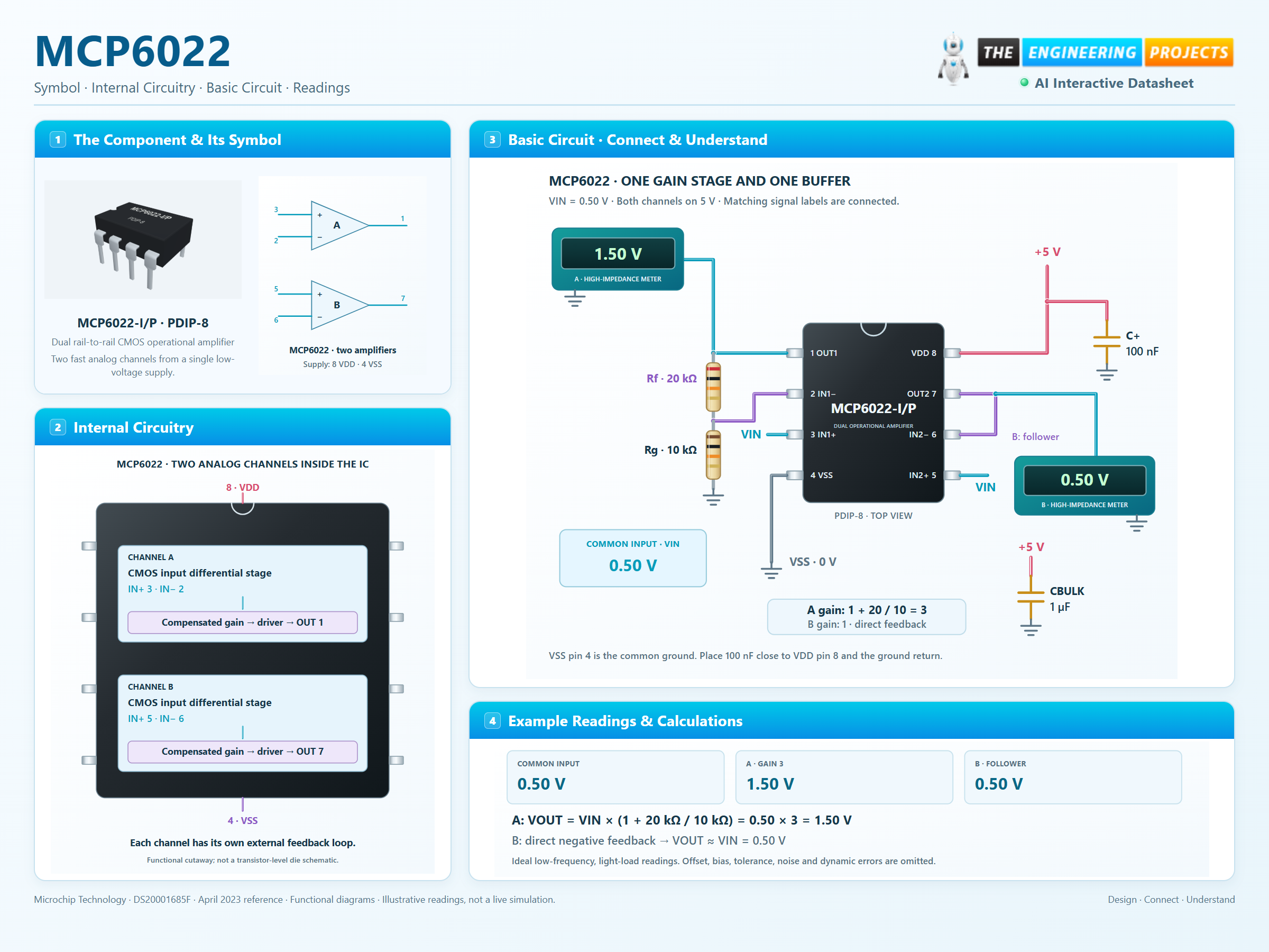
3 stages · Explore one step at a time
Complementary CMOS input paths cover the common-mode range near both supply rails. Their offset and bias behavior still varies with common-mode voltage and temperature; rail-to-rail does not remove input protection limits.
Channel A uses 20 kΩ feedback and 10 kΩ to the common ground, giving a gain of three. Channel B directly feeds its output back to its negative input, giving unity gain.
With a 0.50 V input, the ideal outputs are 1.50 V and 0.50 V. Real output also depends on input offset, resistor accuracy, loading, noise and signal frequency.
A gain-of-three channel beside a unity-gain follower.
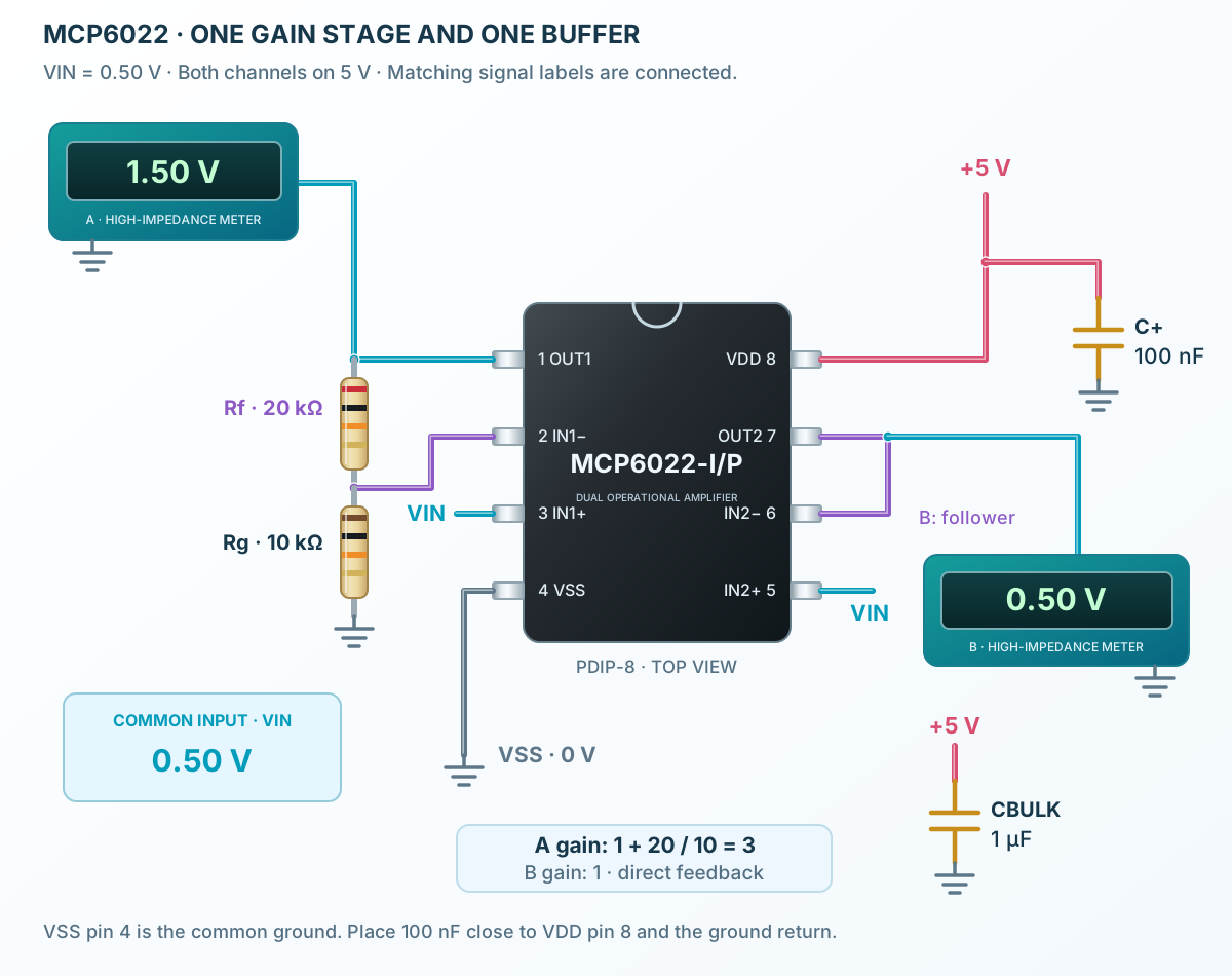
Follow the component values and pin connections
Use +5 V at VDD pin 8 and ground at VSS pin 4, with 100 nF between them.
Add the 20 kΩ / 10 kΩ network to channel A and join pins 7 and 6 for channel B.
At a nominal input of 0.50 V, expect about 1.50 V from A and 0.50 V from B under light DC loading.
Two CMOS input stages, compensated voltage gain and rail-to-rail output drivers.
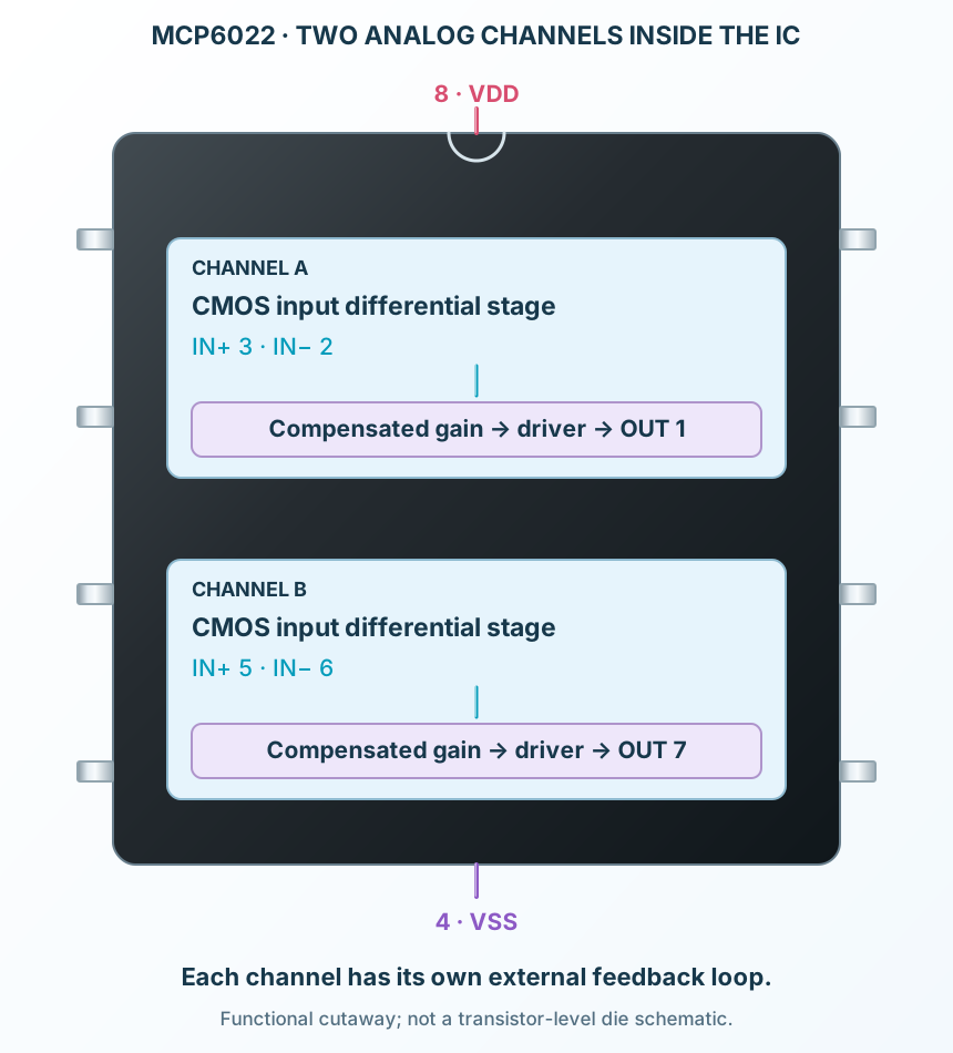
Select a stage to see its role and connections
Complementary CMOS input paths cover the common-mode range near both supply rails. Their offset and bias behavior still varies with common-mode voltage and temperature; rail-to-rail does not remove input protection limits.
Each channel has an internal voltage-gain path and frequency compensation.
Each channel drives a compatible load close to its rails. The remaining headroom depends on load and current direction. The short-circuit current is a fault characteristic, not a normal drive-current promise.
Signal names, electrical functions and connection guidance
Scroll within the table to see all columns and rows.
| Pin | Signal | Type | Function & connection |
|---|---|---|---|
| OUT1 | Analog output | Channel A output.Connection guidanceReturn to IN1− through 20 kΩ; connect a high-impedance meter. | |
| IN1− | Inverting input | Channel A negative-feedback node.Connection guidanceJoin 20 kΩ from OUT1 and 10 kΩ to signal ground. | |
| IN1+ | Non-inverting input | Channel A signal input.Connection guidanceApply VIN = 0.50 V relative to ground. | |
| VSS | Ground return | Supply return shared by both amplifiers.Connection guidanceConnect directly to common ground. | |
| IN2+ | Non-inverting input | Channel B signal input.Connection guidanceConnect to the same VIN in the illustrated follower. | |
| IN2− | Inverting input | Channel B feedback input.Connection guidanceConnect directly to OUT2 pin 7. | |
| OUT2 | Analog output | Channel B output.Connection guidanceConnect to IN2−; leave unloaded or use a high-impedance instrument. | |
| VDD | Positive supply | Positive rail shared by both amplifiers.Connection guidanceConnect +5 V; bypass to ground with 100 nF close to pins 8 and 4. |
No pins match these filters. Try another signal name or reset the filters.
MCP6022-I/P and MCP6022-I/SN
Scroll within the table to see all columns and rows.
| Parameter | Value | Conditions / notes |
|---|---|---|
| Supply span | 2.5–5.5 V | VDD minus VSS |
| Industrial ambient range | −40 to +85°C | Selected I-grade parts |
| Input common-mode interval | VSS − 0.3 V to VDD + 0.3 V | Input voltage and current protection limits still apply |
| Example rails | VDD8 = 5 V; VSS4 = 0 V | Supply return is also signal ground |
| Typical current per amplifier | 1.0 mA | 0.5 mA minimum; 1.35 mA maximum, unloaded at 25°C |
| Nominal two-channel current | 2.0 mA | Before external load current |
| No VREF or chip-select pin | MCP6022 has two amplifiers | Do not apply MCP6021/6023 single-amplifier pin functions |
No specifications match. Try a parameter name or a unit.
Unless stated otherwise, electrical values follow the manufacturer 25°C, 2.5–5.5 V, midsupply signal and 10 kΩ-to-midsupply test conditions.
Industrial grade · 25°C unless stated
Scroll within the table to see all columns and rows.
| Parameter | Value | Conditions / notes |
|---|---|---|
| Input offset voltage | ±500 µV maximum | VCM = 0 V; selected industrial grade |
| Typical offset drift | ±3.5 µV/°C | Characterized over −40 to +125°C |
| Input bias current | 1 pA typical | Room temperature |
| Bias current at +85°C | 30 pA typical; 150 pA maximum | Industrial temperature parts |
| Input offset current | ±1 pA typical | Room temperature |
| CMRR over full common-mode range | 74 dB minimum; 90 dB typical | VDD = 5 V; VCM = −0.3 to 5.3 V |
| Supply rejection | 74 dB minimum; 90 dB typical | VCM = 0 V |
| Open-loop gain | 90 dB minimum; 110 dB typical | VCM = 0; VOUT = VSS + 0.3 to VDD − 0.3 V |
| Output swing endpoints | VSS + 15 mV to VDD − 20 mV | 10 kΩ to midsupply; 0.5 V differential overdrive |
No specifications match. Try a parameter name or a unit.
The swing test uses input overdrive; do not treat its endpoints as precision closed-loop headroom at arbitrary load.
Typical values at manufacturer AC conditions
Scroll within the table to see all columns and rows.
| Parameter | Value | Conditions / notes |
|---|---|---|
| Gain-bandwidth product | 10 MHz | Closed-loop bandwidth depends on noise gain |
| Slew rate | 7.0 V/µs | Large-signal slope limit |
| Phase margin | 65° | Gain +1; CL = 60 pF |
| Settling to 0.2% | 250 ns | Gain +1; 100 mV peak-to-peak output |
| Voltage-noise density | 8.7 nV/√Hz | 10 kHz |
| Integrated low-frequency noise | 2.9 µV peak-to-peak | 0.1–10 Hz |
| Current-noise density | 3 fA/√Hz | 1 kHz |
| THD + noise | 0.00053% | 1 kHz; gain +1; VDD 5 V; output 0.25–3.25 V; 22 kHz bandwidth |
No specifications match. Try a parameter name or a unit.
Small-signal bandwidth, large-signal slew and settling describe different limitations.
A fast CMOS amplifier needs short loops
Scroll within the table to see all columns and rows.
| Parameter | Value | Conditions / notes |
|---|---|---|
| Local bypass | 100 nF in the example | Manufacturer recommends 10–100 nF within 2 mm of VDD |
| Nearby bulk storage | 1 µF or larger | Within 100 mm; may be shared by nearby analog parts |
| Feedback network | Short routes around each input/output pair | The 20 kΩ / 10 kΩ example is a low-frequency demonstration |
| Parasitic capacitance | Check feedback resistance against input and board capacitance | High-frequency noise gain can rise and phase margin can fall |
| Capacitive loads | Choose an isolation network for the actual load | Do not assume stable direct drive of long cables |
| Input leakage | Clean high-impedance nodes | Temperature, moisture and contamination increase errors |
| Unused channel | Stable negative feedback to a valid reference | Do not leave its inputs floating |
No specifications match. Try a parameter name or a unit.
Use the manufacturer capacitive-load and feedback-capacitance guidance for high-frequency designs.
Absolute ratings are not normal operating targets
Scroll within the table to see all columns and rows.
| Parameter | Value | Conditions / notes |
|---|---|---|
| Absolute supply | 7.0 V | Normal operating upper limit is 5.5 V |
| Analog-input current | ±2 mA absolute maximum | Provide the specified protection if inputs can exceed safe voltage limits |
| Output / supply-pin current | ±30 mA absolute maximum | Not a recommended continuous load current |
| Junction / storage | 150°C maximum / −65 to +150°C | Do not substitute these for ambient operating limits |
| Extended E-grade offset | ±250 µV at 25°C, VDD 5 V, VCM 0 V | A different grade; not used as the I-grade limit here |
| Extended E-grade ambient | −40 to +125°C | The selected I-grade page uses −40 to +85°C |
No specifications match. Try a parameter name or a unit.
Power dissipation and board thermal conditions can constrain usable current before an absolute limit is reached.
5 V single supply · common ground
Scroll within the table to see all columns and rows.
| Parameter | Value | Conditions / notes |
|---|---|---|
| Input VIN | 0.50 V | Pins 3 and 5; common signal ground |
| Channel A feedback | 20 kΩ | OUT1 pin 1 to IN1− pin 2 |
| Channel A ground resistor | 10 kΩ | IN1− pin 2 to 0 V |
| Channel A ideal output | 1.50 V | 0.50 × (1 + 20 / 10) |
| Channel B feedback | Direct connection | OUT2 pin 7 to IN2− pin 6 |
| Channel B ideal output | 0.50 V | Unity-gain follower |
| Bypass capacitors | 100 nF | VDD pin 8 to ground pin 4 |
| Bulk bypass | 1 µF minimum | Nearby between +5 V and GND; may be shared |
No specifications match. Try a parameter name or a unit.
The supply return and signal ground are common. Keep the bypass loop short.
MCP6022-I/P · PDIP-8
Scroll within the table to see all columns and rows.
| Parameter | Value | Conditions / notes |
|---|---|---|
| Lead pitch | 2.54 mm | Through-hole |
| Channel A | OUT1 1; IN1− 2; IN1+ 3 | Independent feedback loop |
| Channel B | IN2+ 5; IN2− 6; OUT2 7 | Independent feedback loop |
| Supply | VSS 4; VDD 8 | Shared by both channels |
| Package orientation | Top view; pin 1 at the marker | Counterclockwise numbering |
No specifications match. Try a parameter name or a unit.
This dual-amplifier pinout differs from single amplifiers such as TL081 or LM741.
No matching rowsTry a pin name, parameter, unit or test condition, or reset the filters.
Amplify compatible low-voltage sensor signals while checking bandwidth and ADC settling.
Manufacturer application guideBuild two-channel or cascaded filters with adequate noise-gain and phase-margin allowance.
Manufacturer application guideUse the low-noise dual amplifier with suitable bias, loading and supply bypass.
Manufacturer application guideFind MCP6022 in the Components Library to place its schematic symbol and connect its pins.
Reference page · circuit simulation model not yet availableOpen ProTech