Real View
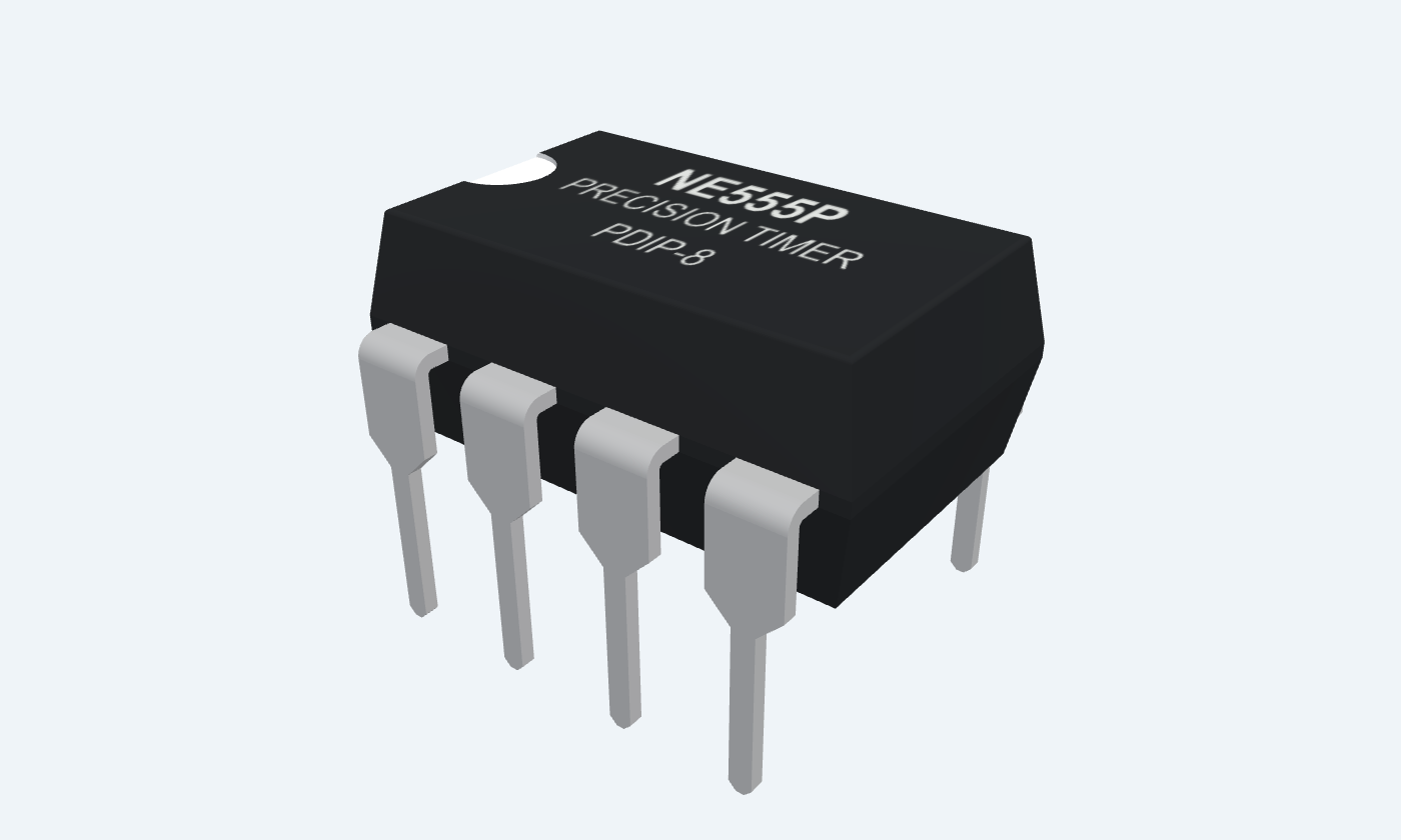
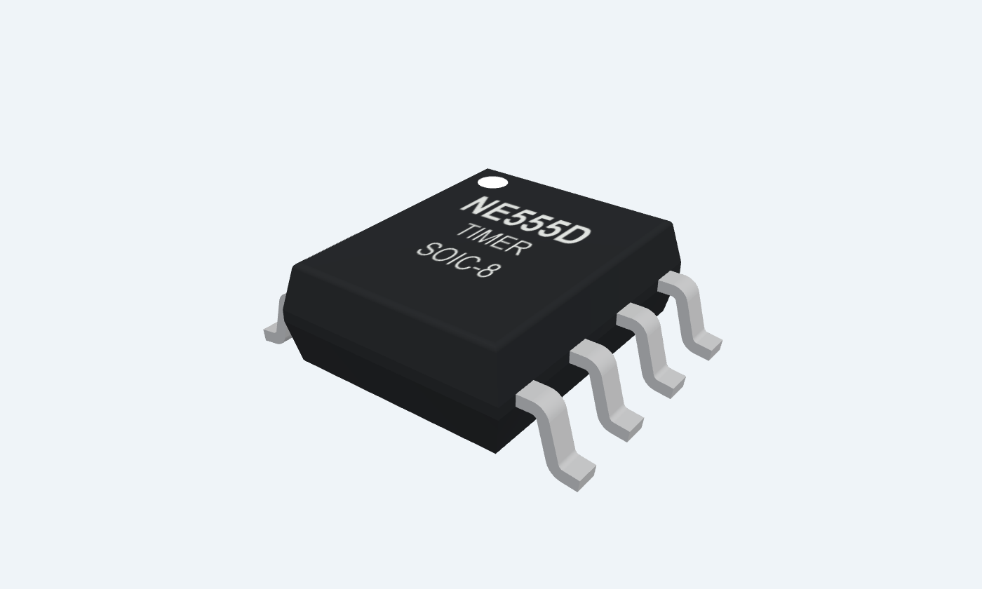
Turn a resistor and capacitor into a clock.
NE555 is an eight-pin timer for repeating pulses or a single timed output. An external resistor-capacitor network sets the timing; internal comparators and a latch control the output. Choose NE555P in PDIP-8 or NE555D in SOIC-8. Both use the same eight-pin mapping. The example is a 5 V astable LED flasher.
Select a pin to explore its connection
Click a lead or use the arrow keys. Top view
Circuit reference.
Connect to supply return.
Starts a timing cycle below roughly VCC/3.
For astable operation, join TRIG to THRES at the capacitor node.
Timer output.
Drive the LED through a current-limiting resistor.
Output is not rail-to-rail; check loading and dissipation.
Active-low reset overrides the timing cycle.
Tie to VCC when reset is unused.
Adjusts comparator reference levels.
A small bypass capacitor to ground reduces noise when control is unused.
Ends the high interval above roughly 2VCC/3.
Connect to the timing capacitor node.
Discharges the timing capacitor during the low interval.
Connect to the junction of the astable timing resistors.
Positive supply.
Use 4.5–16 V, with local supply decoupling.
The capacitor moves between two thresholds, and the output changes state each cycle.
NE555P · PDIP-8
| Property | Details |
|---|---|
| Manufacturer | Texas Instruments |
| Part number | NE555P |
| Package | PDIP-8 |
| Connections | 8 pins |
| Mounting | Through-hole |
| Lead pitch | 2.54 mm |
| Package code | P |
| Thermal reference | See manufacturer thermal table |
Reviewed manufacturer specifications
Scroll sideways to see all columns.
| Parameter | Value | Conditions / notes |
|---|---|---|
| Supply | 4.5–16 V | Recommended for NE555 |
| Ambient | 0–70°C | NE555 grade |
| Output | Up to ±200 mA | Do not ignore output drop or package dissipation |
| Supply absolute maximum | 18 V | Stress limit, not an operating target |
No specifications match. Try a parameter name or a unit.
Reviewed manufacturer specifications
Scroll sideways to see all columns.
| Parameter | Value | Conditions / notes |
|---|---|---|
| High interval | tH ≈ 0.693 (RA + RB) C | Standard astable circuit |
| Low interval | tL ≈ 0.693 RB C | Standard astable circuit |
| Frequency | f ≈ 1.44 / ((RA + 2RB) C) | R in ohms; C in farads |
| Duty cycle | D ≈ (RA + RB) / (RA + 2RB) | Greater than 50% in this basic circuit |
| Single pulse | t ≈ 1.1 RC | Monostable circuit |
No specifications match. Try a parameter name or a unit.
Reviewed manufacturer specifications
Scroll sideways to see all columns.
| Parameter | Value | Conditions / notes |
|---|---|---|
| RA / RB / C | 10 kΩ / 68 kΩ / 10 µF | Illustrative values |
| High time | ≈0.541 s | Calculated ideal interval |
| Low time | ≈0.471 s | Calculated ideal interval |
| Frequency | ≈0.99 Hz | Approximate; tolerance changes the result |
No specifications match. Try a parameter name or a unit.
Select a pin for its function, connection guidance and electrical notes.
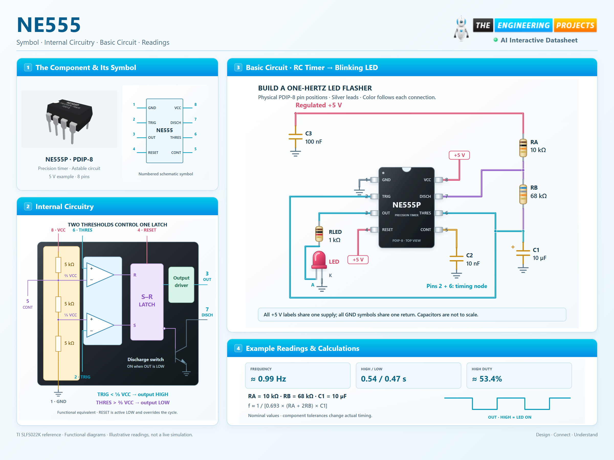
Follow the labeled connections and functional stages
3 stages · Explore one step at a time
Connect pins 8 and 4 to +5 V, pin 1 to ground. Use a 100 nF supply bypass and a 10 nF capacitor from CONT to ground.
RA = 10 kΩ, RB = 68 kΩ and C1 = 10 µF. Join pins 2 and 6 to the capacitor node; pin 7 connects to the resistor junction. The capacitor’s positive plate faces the timing node.
Nominal high time is 0.693 × (RA + RB) × C1 = 0.541 s. Low time is 0.693 × RB × C1 = 0.471 s. The LED flashes about once per second; tolerance changes the exact result.
A complete wiring example with numbered pins, component values and local ground symbols.
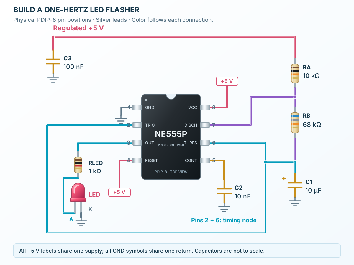
Follow the component values and pin connections
Connect pins 8 and 4 to +5 V, pin 1 to ground. Use a 100 nF supply bypass and a 10 nF capacitor from CONT to ground.
RA = 10 kΩ, RB = 68 kΩ and C1 = 10 µF. Join pins 2 and 6 to the capacitor node; pin 7 connects to the resistor junction. The capacitor’s positive plate faces the timing node.
Nominal high time is 0.693 × (RA + RB) × C1 = 0.541 s. Low time is 0.693 × RB × C1 = 0.471 s. The LED flashes about once per second; tolerance changes the exact result.
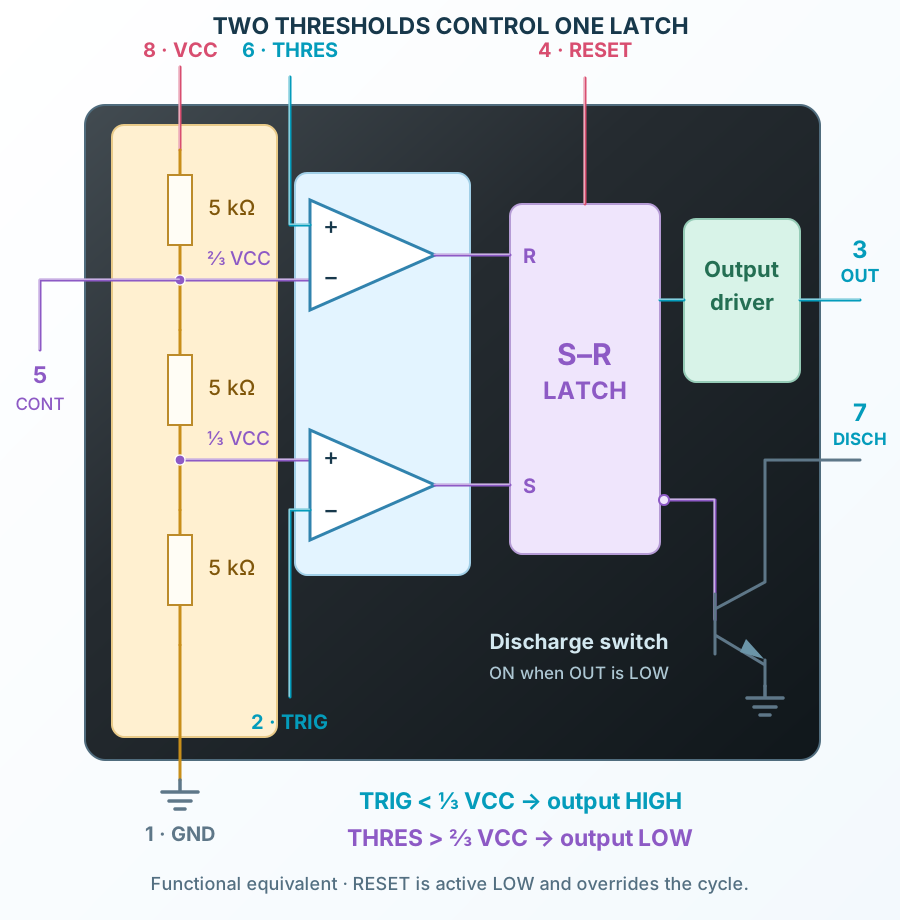
A labeled functional schematic with the important signal paths.
Select a stage to see its role and connections
Three nominal 5 kΩ resistors establish 1/3 and 2/3 of VCC. The control pin provides access to the upper reference.
TRIG below 1/3 VCC sets the latch. THRES above 2/3 VCC resets it. Active-low RESET overrides the timing cycle.
The output stage follows the latch. In the low state, the discharge transistor connects pin 7 toward ground and empties the timing capacitor through RB.
Signal names, electrical functions and connection guidance
Scroll within the table to see all columns and rows.
| Pin | Signal | Type | Function & connection |
|---|---|---|---|
| GND | Ground | Circuit reference.Connection guidanceConnect to supply return. | |
| TRIG | Input | Starts a timing cycle below roughly VCC/3.Connection guidanceFor astable operation, join TRIG to THRES at the capacitor node. | |
| OUT | Output | Timer output.Connection guidanceDrive the LED through a current-limiting resistor. Output is not rail-to-rail; check loading and dissipation. | |
| RESET | Input | Active-low reset overrides the timing cycle.Connection guidanceTie to VCC when reset is unused. | |
| CONT | Control | Adjusts comparator reference levels.Connection guidanceA small bypass capacitor to ground reduces noise when control is unused. | |
| THRES | Input | Ends the high interval above roughly 2VCC/3.Connection guidanceConnect to the timing capacitor node. | |
| DISCH | Open collector | Discharges the timing capacitor during the low interval.Connection guidanceConnect to the junction of the astable timing resistors. | |
| VCC | Power | Positive supply.Connection guidanceUse 4.5–16 V, with local supply decoupling. |
No pins match these filters. Try another signal name or reset the filters.
Reviewed manufacturer specifications
Scroll within the table to see all columns and rows.
| Parameter | Value | Conditions / notes |
|---|---|---|
| Supply | 4.5–16 V | Recommended for NE555 |
| Ambient | 0–70°C | NE555 grade |
| Output | Up to ±200 mA | Do not ignore output drop or package dissipation |
| Supply absolute maximum | 18 V | Stress limit, not an operating target |
No specifications match. Try a parameter name or a unit.
Reviewed manufacturer specifications
Scroll within the table to see all columns and rows.
| Parameter | Value | Conditions / notes |
|---|---|---|
| High interval | tH ≈ 0.693 (RA + RB) C | Standard astable circuit |
| Low interval | tL ≈ 0.693 RB C | Standard astable circuit |
| Frequency | f ≈ 1.44 / ((RA + 2RB) C) | R in ohms; C in farads |
| Duty cycle | D ≈ (RA + RB) / (RA + 2RB) | Greater than 50% in this basic circuit |
| Single pulse | t ≈ 1.1 RC | Monostable circuit |
No specifications match. Try a parameter name or a unit.
Reviewed manufacturer specifications
Scroll within the table to see all columns and rows.
| Parameter | Value | Conditions / notes |
|---|---|---|
| RA / RB / C | 10 kΩ / 68 kΩ / 10 µF | Illustrative values |
| High time | ≈0.541 s | Calculated ideal interval |
| Low time | ≈0.471 s | Calculated ideal interval |
| Frequency | ≈0.99 Hz | Approximate; tolerance changes the result |
No specifications match. Try a parameter name or a unit.
No matching rowsTry a pin name, parameter, unit or test condition, or reset the filters.
A timing network produces regular output pulses. Keep a resistor in series with the LED.
Manufacturer application guideMonostable operation creates one timed interval per valid trigger.
Manufacturer application guideFind NE555 in the Components Library to place its schematic symbol and connect its pins.
Simulation model available · Open the working exampleOpen ProTech