NE556Dual bipolar timer
Two independent clocks. One compact IC.
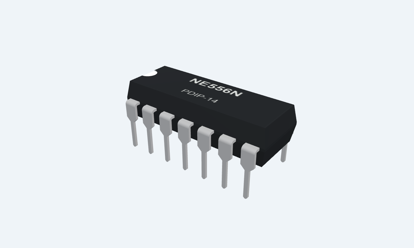
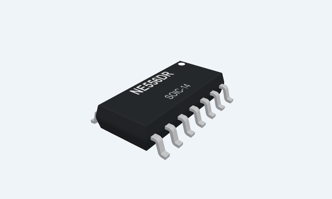
NE556 combines two independently controlled timer circuits in a 14-pin IC. Each channel has its own trigger, threshold, control, reset, output and discharge contact; only the power rails are shared. External resistors and capacitors set a repeating waveform or a single timed pulse. Our two-clock example makes the difference visible: channel 1 cycles slowly while channel 2 runs about ten times faster. The package switch compares NE556N through-hole PDIP-14 with NE556DR SOIC-14. Select any pin to inspect its function, or adjust the two timing networks below to explore the calculated results.

14Physical pins
NE556NPDIP-14
Manufacturer-referencedTexas Instruments
Pin diagram
Select a pin to explore its connection
Highlight
NE556NPDIP-14Top view
NE556DRSOIC-14Top view
Click a lead or use the arrow keys. Top view
PIN 1 · Outputs and discharge
Open-collector discharge1DISCH
Function
Discharges the external timing capacitor when this channel is LOW.
How to connect
Connect to the junction of RA and RB.
Electrical note
This is a switching node, not a second push-pull output.
PIN 2 · Timing inputs
Threshold input1THRES
Function
Ends the HIGH interval when the timing node exceeds the upper reference.
How to connect
Join to 1TRIG and the timing capacitor.
Electrical note
Nominal reference: 2/3 VCC with CONT unmodulated.
PIN 3 · Reset and control
Control voltage1CONT
Function
Sets the comparator reference for timer 1.
How to connect
Bypass to ground with 10 nF in the example.
Electrical note
Changing CONT changes both thresholds and the timing equations.
PIN 4 · Reset and control
Active-low reset1RESET
Function
Forces this output LOW and turns on its discharge switch.
How to connect
Tie to VCC for continuous operation.
Electrical note
Do not leave reset floating; it overrides trigger and threshold.
PIN 5 · Outputs and discharge
Push-pull output1OUT
Function
Timer 1 output, independent of the other channel.
How to connect
Connect a high-impedance scope or a current-limited LED.
Electrical note
Output swing depends on load; it is not rail-to-rail.
PIN 6 · Timing inputs
Trigger input1TRIG
Function
Starts the HIGH interval when the input falls below the lower reference.
How to connect
Join to 1THRES in the astable example.
Electrical note
Nominal reference: 1/3 VCC. A sustained LOW trigger can hold the output HIGH.
PIN 7 · Ground
GroundGND
Function
Common return for both channels.
How to connect
Connect all local ground symbols to supply return.
PIN 8 · Timing inputs
Trigger input2TRIG
Function
Starts the HIGH interval when the input falls below the lower reference.
How to connect
Join to 2THRES in the astable example.
Electrical note
Nominal reference: 1/3 VCC. A sustained LOW trigger can hold the output HIGH.
PIN 9 · Outputs and discharge
Push-pull output2OUT
Function
Timer 2 output, independent of the other channel.
How to connect
Connect a high-impedance scope or a current-limited LED.
Electrical note
Output swing depends on load; it is not rail-to-rail.
PIN 10 · Reset and control
Active-low reset2RESET
Function
Forces this output LOW and turns on its discharge switch.
How to connect
Tie to VCC for continuous operation.
Electrical note
Do not leave reset floating; it overrides trigger and threshold.
PIN 11 · Reset and control
Control voltage2CONT
Function
Sets the comparator reference for timer 2.
How to connect
Bypass to ground with 10 nF in the example.
Electrical note
Changing CONT changes both thresholds and the timing equations.
PIN 12 · Timing inputs
Threshold input2THRES
Function
Ends the HIGH interval when the timing node exceeds the upper reference.
How to connect
Join to 2TRIG and the timing capacitor.
Electrical note
Nominal reference: 2/3 VCC with CONT unmodulated.
PIN 13 · Outputs and discharge
Open-collector discharge2DISCH
Function
Discharges the external timing capacitor when this channel is LOW.
How to connect
Connect to the junction of RA and RB.
Electrical note
This is a switching node, not a second push-pull output.
PIN 14 · Supply
SupplyVCC
Function
Positive supply shared by the two timers.
How to connect
Apply regulated +5 V; place 100 nF directly between pins 14 and 7.
Key specifications
Choose a separate RC network for each timer. Reset can stop either channel while the other continues.
Recommended supply4.5–16 V
Independent timers2 Separate timing networks
Ambient range0–70 °C · NE grade
Physical contacts14 PDIP / SOIC
Package details
NE556N · PDIP-14
| Property | Details |
|---|---|
| Manufacturer | Texas Instruments |
| Part number | NE556N |
| Package | PDIP-14 |
| Connections | 14 pins |
| Mounting | Through-hole |
| Lead pitch | 2.54 mm |
| Package code | dip |
| Thermal reference | Board and package dependent; see manufacturer data |
Operating conditions
NE556 grade
Manufacturer specifications 5 parameters
Scroll sideways to see all columns.
| Parameter | Value | Conditions / notes |
|---|---|---|
| Supply | 4.5–16 V | Recommended operating range |
| Ambient temperature | 0 to +70°C | NE556N / NE556DR |
| Output loading | Up to ±200 mA specified | Check output drop and package dissipation; not a promise of rail-to-rail swing |
| Example supply | 5 V | Common to both channels |
| Local decoupling | 100 nF | Directly across pins 14 and 7 |
No specifications match. Try a parameter name or a unit.
Recommended operation is distinct from absolute stress limits.
Thresholds and output levels
25°C · stated test conditions
Manufacturer specifications 5 parameters
Scroll sideways to see all columns.
| Parameter | Value | Conditions / notes |
|---|---|---|
| Trigger at 5 V | 1.67 V typical; 1.1–2.2 V limits | Each channel |
| Threshold at 5 V | 3.3 V typical; 2.4–4.2 V limits | Each channel |
| LOW output | 0.1 V typical; 0.25 V maximum | 5 V supply; sinking 5 mA |
| HIGH output | 3.3 V typical; 2.75 V minimum | 5 V supply; sourcing 100 mA |
| Supply current | 6 mA typical; 12 mA maximum | 5 V; outputs LOW; no external load |
No specifications match. Try a parameter name or a unit.
These test points must not be extrapolated to every load or temperature.
Timing equations
Nominal RC relationships
Manufacturer specifications 5 parameters
Scroll sideways to see all columns.
| Parameter | Value | Conditions / notes |
|---|---|---|
| Astable HIGH | ln(2) × (RA + RB) × C | Capacitor charges through both resistors |
| Astable LOW | ln(2) × RB × C | Capacitor discharges through RB |
| Frequency | 1 / [ln(2) × (RA + 2RB) × C] | Use Ω, F and seconds |
| HIGH duty cycle | (RA + RB) / (RA + 2RB) | Above 50% in the ordinary two-resistor circuit |
| Monostable pulse | Approximately 1.1 × R × C | Trigger must return HIGH before the timing interval ends |
No specifications match. Try a parameter name or a unit.
Ideal ratios assume unmodulated CONT. The initial power-on interval differs from steady-state cycles.
Two-clock circuit
5 V · independent outputs
Manufacturer specifications 8 parameters
Scroll sideways to see all columns.
| Parameter | Value | Conditions / notes |
|---|---|---|
| RA1 / RA2 | 10 kΩ | VCC to respective DISCH pin |
| RB1 / RB2 | 100 kΩ | DISCH to respective timing node |
| C1 | 10 µF | Timing node 1 to GND; positive terminal to timing node |
| C2 | 1 µF | Timing node 2 to GND; positive terminal to timing node |
| Nominal f1 / f2 | 0.687 Hz / 6.87 Hz | Ideal values; component tolerances omitted |
| HIGH duty cycle | 52.38% | Both channels |
| Control bypass | 10 nF per channel | Pins 3 and 11 to GND |
| Reset | Pins 4 and 10 to +5 V | Neither input floats |
No specifications match. Try a parameter name or a unit.
The illustrated scope is a high-impedance load. Use a series resistor for any LED.
Control behavior
Applied independently to each timer
Manufacturer specifications 5 parameters
Scroll sideways to see all columns.
| Parameter | Value | Conditions / notes |
|---|---|---|
| RESET LOW | OUT LOW; DISCH conducting | Overrides other inputs |
| TRIG below lower reference | OUT HIGH; DISCH open | When RESET is inactive |
| THRES above upper reference | OUT LOW; DISCH conducting | When trigger is above its reference |
| Both timing inputs between references | Retain latch state | Hysteresis prevents chatter in a clean RC cycle |
| Unused channel | Hold RESET LOW and define its inputs | Do not assume floating pins are harmless |
No specifications match. Try a parameter name or a unit.
Input priority follows RESET, then trigger, then threshold.
Package and pin reference
NE556N · PDIP-14
Manufacturer specifications 5 parameters
Scroll sideways to see all columns.
| Parameter | Value | Conditions / notes |
|---|---|---|
| Pitch | 2.54 mm | Through-hole |
| Timer 1 | DISCH 1; THRES 2; CONT 3 | RESET 4; OUT 5; TRIG 6 |
| Timer 2 | TRIG 8; OUT 9; RESET 10 | CONT 11; THRES 12; DISCH 13 |
| Shared power | GND 7; VCC 14 | Never reuse the eight-pin NE555 numbering |
| Orientation | Top view | Pin-one mark and notch identify the numbering |
No specifications match. Try a parameter name or a unit.
Match the exact mechanical package before manufacturing a PCB.
Connections by function
Select a pin for its function, connection guidance and electrical notes.
Outputs and discharge4 pins
Timing inputs4 pins
Reset and control4 pins
Ground1 pin
Supply1 pin
Outputs and discharge4 pins
Timing inputs4 pins
Reset and control4 pins
Ground1 pin
Supply1 pin
NE556 at a glance
Follow the labeled connections and functional stages
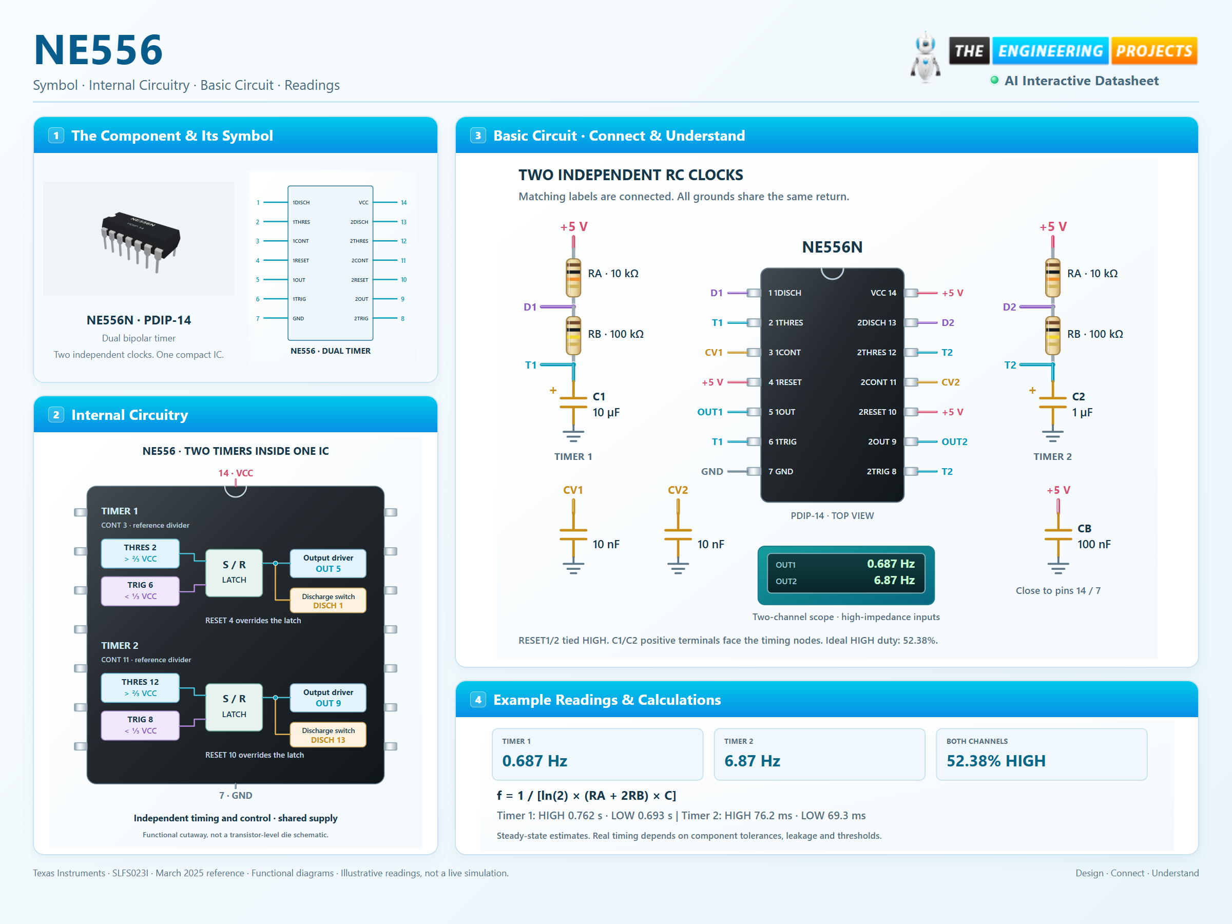
How it works
3 stages · Explore one step at a time
Charge a timing capacitor
With the discharge switch open, each capacitor charges through its RA + RB network. The output remains HIGH until the upper threshold is reached.
Discharge and repeat
The latch then drives the output LOW and connects DISCH to ground. The capacitor discharges through RB until the lower threshold starts another cycle.
Run both channels independently
The two networks share power, not a clock. Using 10 µF for channel 1 and 1 µF for channel 2 with equal resistors gives approximately a ten-to-one frequency ratio. They are not synchronized.
Step 1 of 3
Two timing networks. Two waveforms.
Adjust each channel and compare its ideal steady-state timing.
Timer 1 OUT · pin 5
——
——
Timer 2 OUT · pin 9
——
——
Supply: 5 V. Each graph uses its own time scale. Nominal astable timing, not an electrical simulation. Output amplitudes, tolerances, leakage, startup and loading are not modeled. Both RESET inputs are assumed HIGH; CONT is unmodulated.
NE556 in a circuit
One physical IC, two RC networks and two independent outputs.
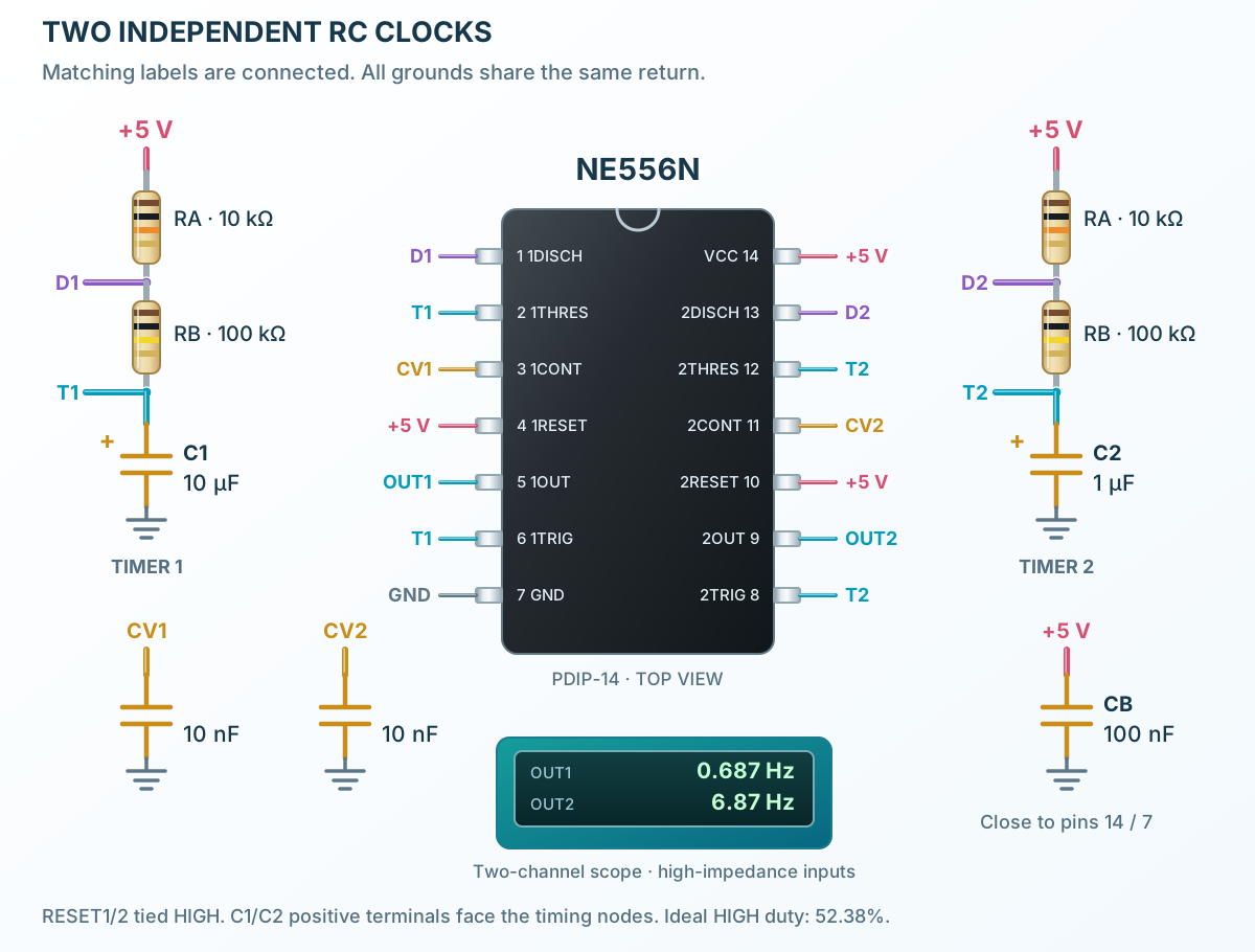
Connect it, step by step
Follow the component values and pin connections
Build two timing networks
Connect each RA to +5 V, each RB between DISCH and its capacitor node, and join TRIG and THRES at that node.
Define the control pins
Tie both RESET contacts HIGH and bypass each CONT input to ground with 10 nF.
Compare the two waveforms
A two-channel high-impedance scope sees approximately 0.69 Hz and 6.87 Hz with the illustrated ideal values.
Inside NE556
Two timer channels inside one package outline.
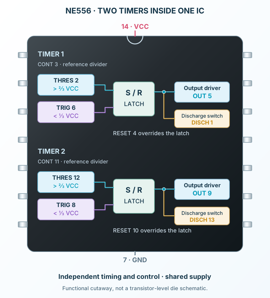
Explore the circuit
Select a stage to see its role and connections
Compare the timing voltage
Two reference levels determine when each channel changes state.
Remember the state
A separate latch per channel controls its output and discharge switch.
Share the supply only
A common bypass capacitor serves VCC and GND; timing and reset remain independent.
Selected packagePDIP-14NE556N
Physical connections14 pinsPackage-specific numbering
Reference collection7 tables33 parameters & pin functions
Pin reference
Signal names, electrical functions and connection guidance
Physical pin numbers14 pins
Scroll within the table to see all columns and rows.
| Pin | Signal | Type | Function & connection |
|---|---|---|---|
| 1DISCH | Open-collector discharge | Discharges the external timing capacitor when this channel is LOW.Connection guidanceConnect to the junction of RA and RB. This is a switching node, not a second push-pull output. | |
| 1THRES | Threshold input | Ends the HIGH interval when the timing node exceeds the upper reference.Connection guidanceJoin to 1TRIG and the timing capacitor. Nominal reference: 2/3 VCC with CONT unmodulated. | |
| 1CONT | Control voltage | Sets the comparator reference for timer 1.Connection guidanceBypass to ground with 10 nF in the example. Changing CONT changes both thresholds and the timing equations. | |
| 1RESET | Active-low reset | Forces this output LOW and turns on its discharge switch.Connection guidanceTie to VCC for continuous operation. Do not leave reset floating; it overrides trigger and threshold. | |
| 1OUT | Push-pull output | Timer 1 output, independent of the other channel.Connection guidanceConnect a high-impedance scope or a current-limited LED. Output swing depends on load; it is not rail-to-rail. | |
| 1TRIG | Trigger input | Starts the HIGH interval when the input falls below the lower reference.Connection guidanceJoin to 1THRES in the astable example. Nominal reference: 1/3 VCC. A sustained LOW trigger can hold the output HIGH. | |
| GND | Ground | Common return for both channels.Connection guidanceConnect all local ground symbols to supply return. | |
| 2TRIG | Trigger input | Starts the HIGH interval when the input falls below the lower reference.Connection guidanceJoin to 2THRES in the astable example. Nominal reference: 1/3 VCC. A sustained LOW trigger can hold the output HIGH. | |
| 2OUT | Push-pull output | Timer 2 output, independent of the other channel.Connection guidanceConnect a high-impedance scope or a current-limited LED. Output swing depends on load; it is not rail-to-rail. | |
| 2RESET | Active-low reset | Forces this output LOW and turns on its discharge switch.Connection guidanceTie to VCC for continuous operation. Do not leave reset floating; it overrides trigger and threshold. | |
| 2CONT | Control voltage | Sets the comparator reference for timer 2.Connection guidanceBypass to ground with 10 nF in the example. Changing CONT changes both thresholds and the timing equations. | |
| 2THRES | Threshold input | Ends the HIGH interval when the timing node exceeds the upper reference.Connection guidanceJoin to 2TRIG and the timing capacitor. Nominal reference: 2/3 VCC with CONT unmodulated. | |
| 2DISCH | Open-collector discharge | Discharges the external timing capacitor when this channel is LOW.Connection guidanceConnect to the junction of RA and RB. This is a switching node, not a second push-pull output. | |
| VCC | Supply | Positive supply shared by the two timers.Connection guidanceApply regulated +5 V; place 100 nF directly between pins 14 and 7. |
No pins match these filters. Try another signal name or reset the filters.
Operating conditions
NE556 grade
Manufacturer-referenced values5 parameters
Scroll within the table to see all columns and rows.
| Parameter | Value | Conditions / notes |
|---|---|---|
| Supply | 4.5–16 V | Recommended operating range |
| Ambient temperature | 0 to +70°C | NE556N / NE556DR |
| Output loading | Up to ±200 mA specified | Check output drop and package dissipation; not a promise of rail-to-rail swing |
| Example supply | 5 V | Common to both channels |
| Local decoupling | 100 nF | Directly across pins 14 and 7 |
No specifications match. Try a parameter name or a unit.
Recommended operation is distinct from absolute stress limits.
Thresholds and output levels
25°C · stated test conditions
Manufacturer-referenced values5 parameters
Scroll within the table to see all columns and rows.
| Parameter | Value | Conditions / notes |
|---|---|---|
| Trigger at 5 V | 1.67 V typical; 1.1–2.2 V limits | Each channel |
| Threshold at 5 V | 3.3 V typical; 2.4–4.2 V limits | Each channel |
| LOW output | 0.1 V typical; 0.25 V maximum | 5 V supply; sinking 5 mA |
| HIGH output | 3.3 V typical; 2.75 V minimum | 5 V supply; sourcing 100 mA |
| Supply current | 6 mA typical; 12 mA maximum | 5 V; outputs LOW; no external load |
No specifications match. Try a parameter name or a unit.
These test points must not be extrapolated to every load or temperature.
Timing equations
Nominal RC relationships
Manufacturer-referenced values5 parameters
Scroll within the table to see all columns and rows.
| Parameter | Value | Conditions / notes |
|---|---|---|
| Astable HIGH | ln(2) × (RA + RB) × C | Capacitor charges through both resistors |
| Astable LOW | ln(2) × RB × C | Capacitor discharges through RB |
| Frequency | 1 / [ln(2) × (RA + 2RB) × C] | Use Ω, F and seconds |
| HIGH duty cycle | (RA + RB) / (RA + 2RB) | Above 50% in the ordinary two-resistor circuit |
| Monostable pulse | Approximately 1.1 × R × C | Trigger must return HIGH before the timing interval ends |
No specifications match. Try a parameter name or a unit.
Ideal ratios assume unmodulated CONT. The initial power-on interval differs from steady-state cycles.
Two-clock circuit
5 V · independent outputs
Manufacturer-referenced values8 parameters
Scroll within the table to see all columns and rows.
| Parameter | Value | Conditions / notes |
|---|---|---|
| RA1 / RA2 | 10 kΩ | VCC to respective DISCH pin |
| RB1 / RB2 | 100 kΩ | DISCH to respective timing node |
| C1 | 10 µF | Timing node 1 to GND; positive terminal to timing node |
| C2 | 1 µF | Timing node 2 to GND; positive terminal to timing node |
| Nominal f1 / f2 | 0.687 Hz / 6.87 Hz | Ideal values; component tolerances omitted |
| HIGH duty cycle | 52.38% | Both channels |
| Control bypass | 10 nF per channel | Pins 3 and 11 to GND |
| Reset | Pins 4 and 10 to +5 V | Neither input floats |
No specifications match. Try a parameter name or a unit.
The illustrated scope is a high-impedance load. Use a series resistor for any LED.
Control behavior
Applied independently to each timer
Manufacturer-referenced values5 parameters
Scroll within the table to see all columns and rows.
| Parameter | Value | Conditions / notes |
|---|---|---|
| RESET LOW | OUT LOW; DISCH conducting | Overrides other inputs |
| TRIG below lower reference | OUT HIGH; DISCH open | When RESET is inactive |
| THRES above upper reference | OUT LOW; DISCH conducting | When trigger is above its reference |
| Both timing inputs between references | Retain latch state | Hysteresis prevents chatter in a clean RC cycle |
| Unused channel | Hold RESET LOW and define its inputs | Do not assume floating pins are harmless |
No specifications match. Try a parameter name or a unit.
Input priority follows RESET, then trigger, then threshold.
Package and pin reference
NE556N · PDIP-14
Manufacturer-referenced values5 parameters
Scroll within the table to see all columns and rows.
| Parameter | Value | Conditions / notes |
|---|---|---|
| Pitch | 2.54 mm | Through-hole |
| Timer 1 | DISCH 1; THRES 2; CONT 3 | RESET 4; OUT 5; TRIG 6 |
| Timer 2 | TRIG 8; OUT 9; RESET 10 | CONT 11; THRES 12; DISCH 13 |
| Shared power | GND 7; VCC 14 | Never reuse the eight-pin NE555 numbering |
| Orientation | Top view | Pin-one mark and notch identify the numbering |
No specifications match. Try a parameter name or a unit.
Match the exact mechanical package before manufacturing a PCB.
No matching rowsTry a pin name, parameter, unit or test condition, or reset the filters.
Independent pulse generators
Generate two low-frequency timing signals from separate networks.
Manufacturer application guideSequential timers
Use one channel to initiate another with a correctly shaped trigger pulse.
Manufacturer application guidePulse shaping
Configure either timer as a one-shot with a defined trigger and reset path.
Manufacturer application guideTake it into ProTech
Find NE556 in the Components Library to place its schematic symbol and connect its pins.
Reference page · circuit simulation model not yet availableOpen ProTech