PC817Phototransistor optocoupler
Pass the signal with light. Keep the two circuits electrically separate.
PC817 is a four-pin optocoupler with an infrared LED and an NPN phototransistor inside one package. Light carries the signal across the insulating barrier; there is no internal conductive connection between the two sides. This page follows Sharp’s PC817X1 rank A parts in through-hole and gullwing SMD packages. Their current-transfer ratio is 80–160% at 5 mA LED current, 5 V collector-emitter voltage and 25°C; other PC817 grades have different ranges. A series resistor controls LED current, while a separate supply and pull-up create the output signal. The illustrated common-emitter circuit inverts the input and preserves separate input and output grounds.
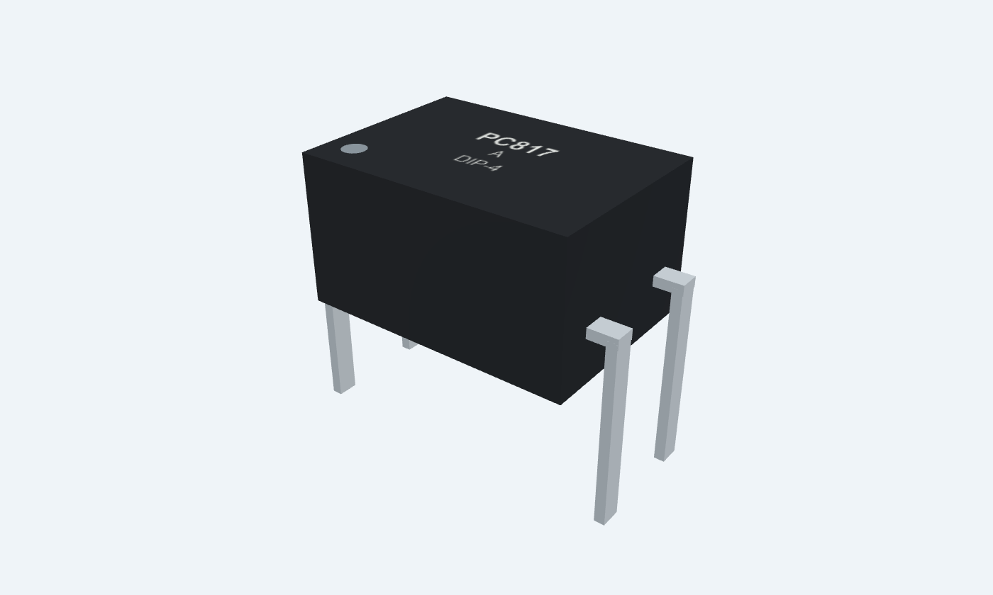
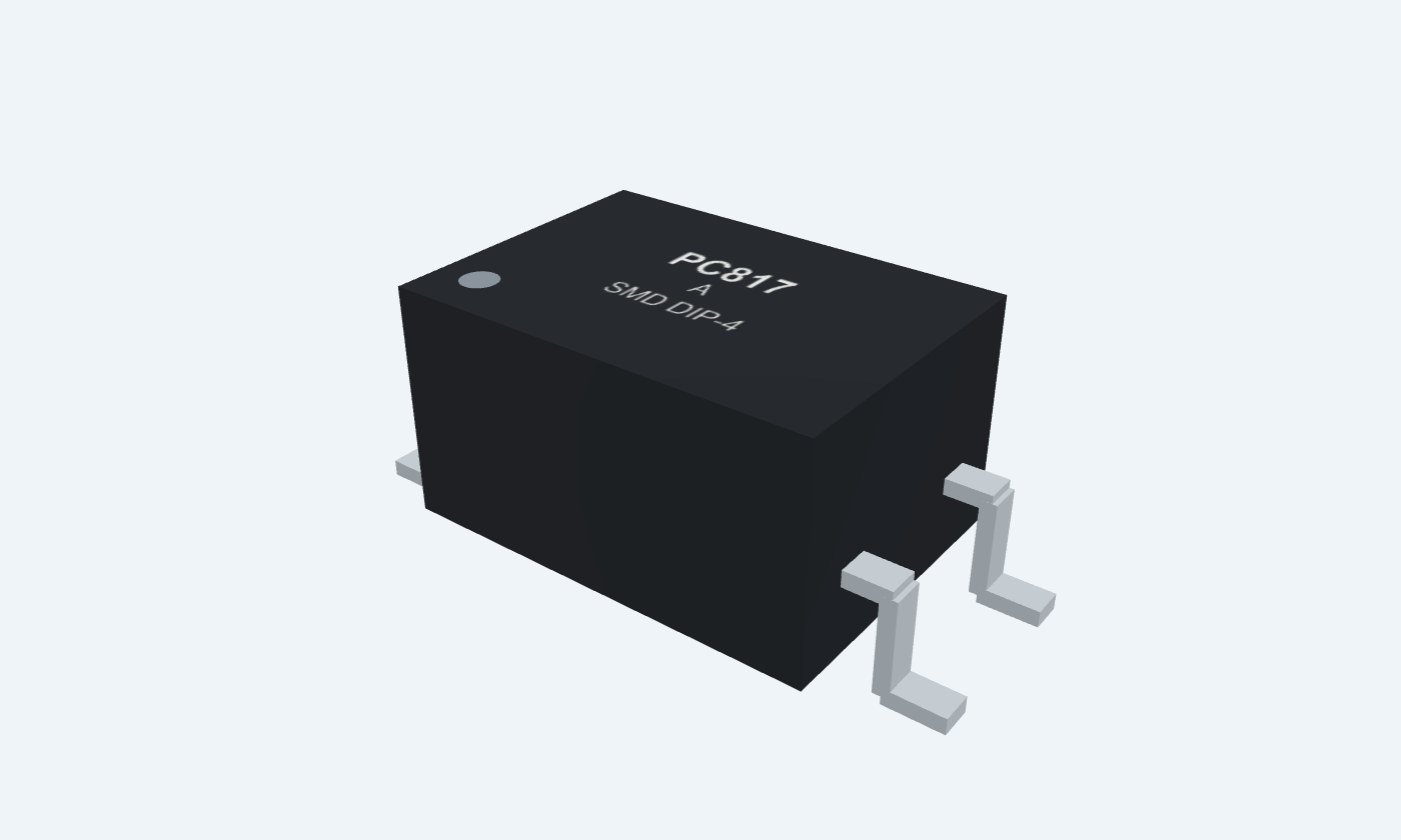

4Physical pins
PC817X1NSZ1BDIP-4
Manufacturer-referencedSharp
Pin diagram
Select a pin to explore its connection
Highlight
PC817DIP-4Top view · pin 1 at the marked corner
PC817SMD DIP-4Top view · pin 1 at the marked corner
Click a lead or use the arrow keys. Top view · pin 1 at the marked corner
PIN 1 · Infrared input
LED anodeA
Function
Positive terminal of the internal infrared emitter. Forward current produces the light that controls the output transistor.
How to connect
Drive through a current-limiting resistor from the input circuit.
Electrical note
Select resistance from the input voltage and forward voltage; never connect directly across a voltage source.
PIN 2 · Infrared input
LED cathodeK
Function
Negative terminal of the infrared emitter.
How to connect
Return to the input-side ground or input driver.
Electrical note
This is not internally connected to the output emitter or its ground.
PIN 3 · Isolated output
Phototransistor emitterE
Function
Emitter of the isolated NPN phototransistor.
How to connect
For the common-emitter example, return to the output-side ground.
Electrical note
There is no base pin. Light from the input emitter controls collector current.
PIN 4 · Isolated output
Phototransistor collectorC
Function
Collector of the isolated NPN phototransistor.
How to connect
Connect a pull-up resistor to the output-side supply; take the output signal from this node.
Electrical note
Light increases collector conduction and pulls the common-emitter output low. The output needs its own supply.
Key specifications
The infrared emitter drives a phototransistor through light. Input current, CTR, pull-up resistance and temperature determine the output behavior.
Electrical terminals4 LED + phototransistor
Selected rank A CTR80–160 % · stated test conditions
Operating ambient−30–100 °C · derating applies
Isolation test5 kVrms · 1 minute
Package details
PC817X1NSZ1B · DIP-4
| Property | Details |
|---|---|
| Manufacturer | Sharp |
| Part number | PC817X1NSZ1B |
| Package | DIP-4 |
| Connections | 4 pins |
| Mounting | Through-hole |
| Lead pitch | 2.54 mm |
| Package code | DIP |
| Thermal reference | Derate LED, collector and total dissipation with ambient temperature |
Selected devices and pinout
One gain grade · two lead forms
Manufacturer specifications 6 parameters
Scroll sideways to see all columns.
| Parameter | Value | Conditions / notes |
|---|---|---|
| Through-hole part | PC817X1NSZ1B | Rank A · four-pin DIP |
| SMD part | PC817X1NIP1B | Rank A · SMT gullwing DIP, not SOP-4 |
| Pin 1 / pin 2 | Anode / cathode | Input infrared LED |
| Pin 4 / pin 3 | Collector / emitter | Output phototransistor |
| CTR for selected rank A | 80–160% | Calculated from 4–8 mA collector current at IF = 5 mA, VCE = 5 V, 25°C |
| Isolation test | 5 kVrms for 1 minute | 40–60% RH; not a continuous working-voltage rating |
No specifications match. Try a parameter name or a unit.
Confirm the complete order code. PC817 variants and manufacturers need not have identical gain or limits.
Electrical characteristics
Sharp test conditions · 25°C
Manufacturer specifications 6 parameters
Scroll sideways to see all columns.
| Parameter | Value | Conditions / notes |
|---|---|---|
| LED forward voltage | 1.2 V typical; 1.4 V maximum | IF = 20 mA |
| LED reverse current | 10 µA maximum | VR = 4 V |
| Collector dark current | 100 nA maximum | VCE = 50 V; IF = 0 |
| Collector saturation voltage | 0.1 V typical; 0.2 V maximum | IF = 20 mA; IC = 1 mA |
| Input capacitance | 30 pF typical; 250 pF maximum | V = 0; f = 1 kHz |
| Input-output capacitance | 0.6 pF typical; 1.0 pF maximum | V = 0; f = 1 MHz |
No specifications match. Try a parameter name or a unit.
Forward voltage varies with current and temperature. CTR measured at VCE = 5 V does not guarantee the same transfer in saturation.
Response and loading
Load-dependent phototransistor response
Manufacturer specifications 6 parameters
Scroll sideways to see all columns.
| Parameter | Value | Conditions / notes |
|---|---|---|
| Rise time | 4 µs typical; 18 µs maximum | VCE = 2 V; IC = 2 mA; RL = 100 Ω |
| Fall time | 3 µs typical; 18 µs maximum | Same response-time test |
| Cut-off frequency | 80 kHz typical | VCE = 5 V; IC = 2 mA; RL = 100 Ω; −3 dB |
| Output pull-up | Lower resistance demands more collector current | Higher resistance increases sensitivity to leakage and capacitance |
| Deep saturation | Can slow turn-off | Account for stored charge in switching designs |
| High-speed protocols | Use a suitable logic-output isolator when needed | The 80 kHz test is not a guaranteed digital data rate |
No specifications match. Try a parameter name or a unit.
The example uses a 10 kΩ pull-up and therefore does not inherit the 100 Ω switching-time test results.
Isolated logic input
5 V input side · separate 3.3 V output side
Manufacturer specifications 6 parameters
Scroll sideways to see all columns.
| Parameter | Value | Conditions / notes |
|---|---|---|
| Input resistance | 750 Ω | Example assumes an approximately 1.2 V LED drop |
| Estimated LED current | 5.07 mA | (5 − 1.2) / 750 |
| Input resistor dissipation | Approximately 19.3 mW | IF² × R; 0.125 W or greater nominal rating provides margin |
| Output pull-up | 10 kΩ to +3.3 V_B | Collector pin 4 is the output node |
| Low-state pull-up current | Up to approximately 0.33 mA | 3.3 V / 10 kΩ, ignoring VCE(sat) |
| Grounds | GND_A and GND_B stay separate | No conductive link across the optocoupler |
No specifications match. Try a parameter name or a unit.
Illustrative low-voltage circuit: verify CTR across temperature and life, logic thresholds, drive capability and switching speed for the actual design.
Absolute maximum ratings
Stress limits at 25°C unless specified
Manufacturer specifications 7 parameters
Scroll sideways to see all columns.
| Parameter | Value | Conditions / notes |
|---|---|---|
| Continuous LED current | 50 mA | Derate with ambient temperature |
| LED reverse voltage | 6 V | Avoid reverse stress in normal operation |
| Collector-emitter voltage | 80 V | LED off |
| Emitter-collector voltage | 6 V | Reverse output polarity limit |
| Collector current | 50 mA | Also limited by power dissipation and temperature |
| LED / collector / total dissipation | 70 / 150 / 200 mW | At 25°C; derating required |
| Operating / storage temperature | −30–100°C / −55–125°C | Ambient operation / unpowered storage |
No specifications match. Try a parameter name or a unit.
These are stress limits, not recommended continuous operating targets. Isolation-system design also depends on spacing, insulation and applicable standards.
Package and PCB geometry
Same electrical numbering in both packages
Manufacturer specifications 6 parameters
Scroll sideways to see all columns.
| Parameter | Value | Conditions / notes |
|---|---|---|
| Moulded body | 6.5 × 4.6 mm nominal | 3.5 mm nominal body height |
| Lead pitch | 2.54 mm | Along each two-pin row |
| DIP footprint | 7.62 mm row spacing | TEP pattern: 1.00 mm holes and 1.80 mm pads |
| SMD footprint | 8.20 mm pad-row centres | Sharp reference pads: 2.20 × 1.70 mm |
| Pin 1 identification | Anode mark on body | Square through-hole pad / top-left SMD mark |
| Board routing | Preserve separation across the barrier | Avoid copper that bypasses the intended isolation |
No specifications match. Try a parameter name or a unit.
Dimensions follow Sharp’s mechanical drawings; check the ordered lead form and your fabricator’s tolerances.
Connections by function
Select a pin for its function, connection guidance and electrical notes.
Infrared input2 pins
Isolated output2 pins
Infrared input2 pins
Isolated output2 pins
PC817 at a glance
Follow the labeled connections and functional stages
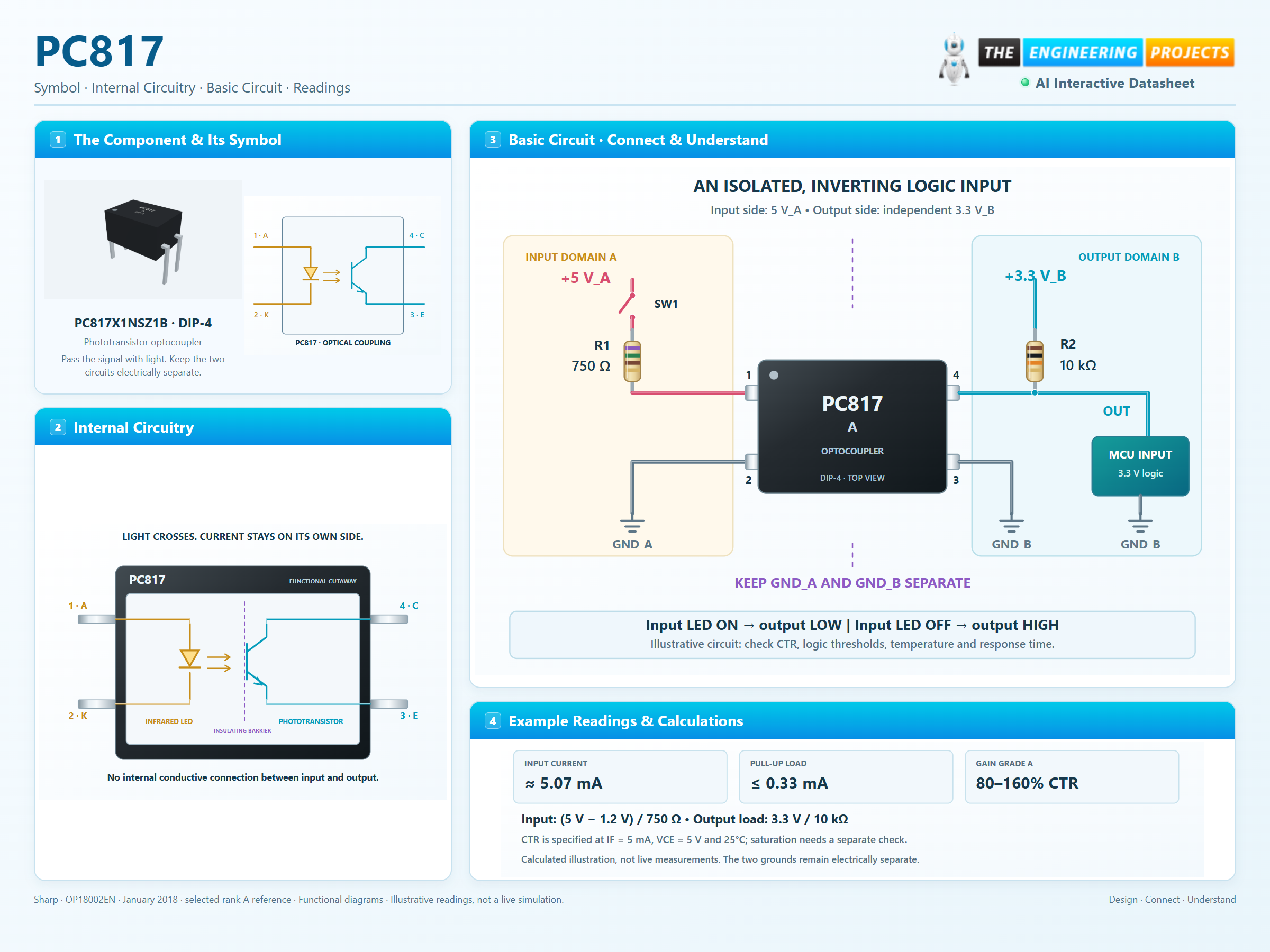
How it works
3 stages · Explore one step at a time
Turn current into light
Input current flows from anode to cathode through the internal infrared LED. The resistor limits that current.
Cross the insulating barrier
Photons reach the output transistor. No wire or shared ground is needed across the barrier.
Turn light into an output level
The transistor sinks current from the output pull-up. With the LED off, the pull-up restores a high level; with sufficient drive, the output goes low.
Step 1 of 3
PC817 in a circuit
Physical package, two supplies and two separate grounds.
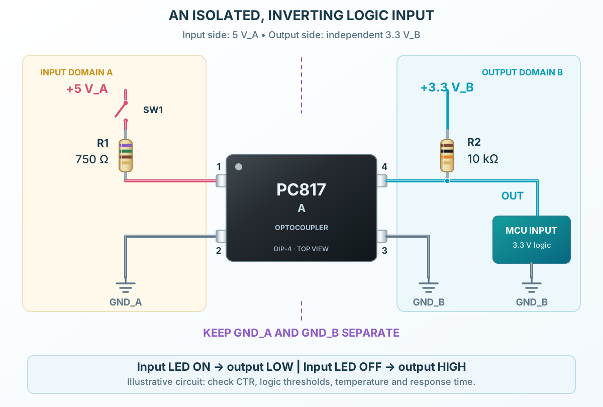
Connect it, step by step
Follow the component values and pin connections
Limit input current
Drive the anode through 750 Ω; return the cathode only to GND_A.
Power the output side
Pull the collector up to the independently powered 3.3 V_B rail through 10 kΩ.
Read the inverted signal
Connect the collector to the receiving logic input and the emitter to GND_B. Check the receiver’s logic thresholds.
Inside PC817
Infrared emitter and phototransistor inside the four-pin body.
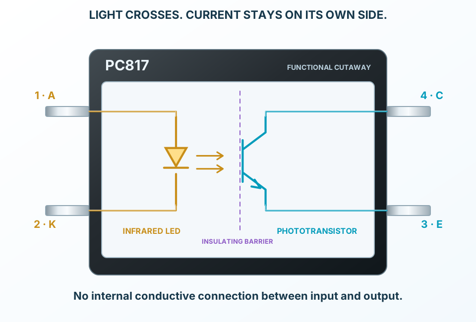
Explore the circuit
Select a stage to see its role and connections
Input emitter
Pins 1 and 2 form the infrared LED. A series resistor sets its current.
Insulating barrier
The input and output have no internal electrical connection.
Output detector
Pins 4 and 3 expose the phototransistor collector and emitter. The base is internal.
Selected packageDIP-4PC817X1NSZ1B
Physical connections4 pinsPackage-specific numbering
Reference collection7 tables37 parameters & pin functions
Pin reference
Signal names, electrical functions and connection guidance
Physical pin numbers4 pins
Scroll within the table to see all columns and rows.
| Pin | Signal | Type | Function & connection |
|---|---|---|---|
| A | LED anode | Positive terminal of the internal infrared emitter. Forward current produces the light that controls the output transistor.Connection guidanceDrive through a current-limiting resistor from the input circuit. Select resistance from the input voltage and forward voltage; never connect directly across a voltage source. | |
| K | LED cathode | Negative terminal of the infrared emitter.Connection guidanceReturn to the input-side ground or input driver. This is not internally connected to the output emitter or its ground. | |
| E | Phototransistor emitter | Emitter of the isolated NPN phototransistor.Connection guidanceFor the common-emitter example, return to the output-side ground. There is no base pin. Light from the input emitter controls collector current. | |
| C | Phototransistor collector | Collector of the isolated NPN phototransistor.Connection guidanceConnect a pull-up resistor to the output-side supply; take the output signal from this node. Light increases collector conduction and pulls the common-emitter output low. The output needs its own supply. |
No pins match these filters. Try another signal name or reset the filters.
Selected devices and pinout
One gain grade · two lead forms
Manufacturer-referenced values6 parameters
Scroll within the table to see all columns and rows.
| Parameter | Value | Conditions / notes |
|---|---|---|
| Through-hole part | PC817X1NSZ1B | Rank A · four-pin DIP |
| SMD part | PC817X1NIP1B | Rank A · SMT gullwing DIP, not SOP-4 |
| Pin 1 / pin 2 | Anode / cathode | Input infrared LED |
| Pin 4 / pin 3 | Collector / emitter | Output phototransistor |
| CTR for selected rank A | 80–160% | Calculated from 4–8 mA collector current at IF = 5 mA, VCE = 5 V, 25°C |
| Isolation test | 5 kVrms for 1 minute | 40–60% RH; not a continuous working-voltage rating |
No specifications match. Try a parameter name or a unit.
Confirm the complete order code. PC817 variants and manufacturers need not have identical gain or limits.
Electrical characteristics
Sharp test conditions · 25°C
Manufacturer-referenced values6 parameters
Scroll within the table to see all columns and rows.
| Parameter | Value | Conditions / notes |
|---|---|---|
| LED forward voltage | 1.2 V typical; 1.4 V maximum | IF = 20 mA |
| LED reverse current | 10 µA maximum | VR = 4 V |
| Collector dark current | 100 nA maximum | VCE = 50 V; IF = 0 |
| Collector saturation voltage | 0.1 V typical; 0.2 V maximum | IF = 20 mA; IC = 1 mA |
| Input capacitance | 30 pF typical; 250 pF maximum | V = 0; f = 1 kHz |
| Input-output capacitance | 0.6 pF typical; 1.0 pF maximum | V = 0; f = 1 MHz |
No specifications match. Try a parameter name or a unit.
Forward voltage varies with current and temperature. CTR measured at VCE = 5 V does not guarantee the same transfer in saturation.
Response and loading
Load-dependent phototransistor response
Manufacturer-referenced values6 parameters
Scroll within the table to see all columns and rows.
| Parameter | Value | Conditions / notes |
|---|---|---|
| Rise time | 4 µs typical; 18 µs maximum | VCE = 2 V; IC = 2 mA; RL = 100 Ω |
| Fall time | 3 µs typical; 18 µs maximum | Same response-time test |
| Cut-off frequency | 80 kHz typical | VCE = 5 V; IC = 2 mA; RL = 100 Ω; −3 dB |
| Output pull-up | Lower resistance demands more collector current | Higher resistance increases sensitivity to leakage and capacitance |
| Deep saturation | Can slow turn-off | Account for stored charge in switching designs |
| High-speed protocols | Use a suitable logic-output isolator when needed | The 80 kHz test is not a guaranteed digital data rate |
No specifications match. Try a parameter name or a unit.
The example uses a 10 kΩ pull-up and therefore does not inherit the 100 Ω switching-time test results.
Isolated logic input
5 V input side · separate 3.3 V output side
Manufacturer-referenced values6 parameters
Scroll within the table to see all columns and rows.
| Parameter | Value | Conditions / notes |
|---|---|---|
| Input resistance | 750 Ω | Example assumes an approximately 1.2 V LED drop |
| Estimated LED current | 5.07 mA | (5 − 1.2) / 750 |
| Input resistor dissipation | Approximately 19.3 mW | IF² × R; 0.125 W or greater nominal rating provides margin |
| Output pull-up | 10 kΩ to +3.3 V_B | Collector pin 4 is the output node |
| Low-state pull-up current | Up to approximately 0.33 mA | 3.3 V / 10 kΩ, ignoring VCE(sat) |
| Grounds | GND_A and GND_B stay separate | No conductive link across the optocoupler |
No specifications match. Try a parameter name or a unit.
Illustrative low-voltage circuit: verify CTR across temperature and life, logic thresholds, drive capability and switching speed for the actual design.
Absolute maximum ratings
Stress limits at 25°C unless specified
Manufacturer-referenced values7 parameters
Scroll within the table to see all columns and rows.
| Parameter | Value | Conditions / notes |
|---|---|---|
| Continuous LED current | 50 mA | Derate with ambient temperature |
| LED reverse voltage | 6 V | Avoid reverse stress in normal operation |
| Collector-emitter voltage | 80 V | LED off |
| Emitter-collector voltage | 6 V | Reverse output polarity limit |
| Collector current | 50 mA | Also limited by power dissipation and temperature |
| LED / collector / total dissipation | 70 / 150 / 200 mW | At 25°C; derating required |
| Operating / storage temperature | −30–100°C / −55–125°C | Ambient operation / unpowered storage |
No specifications match. Try a parameter name or a unit.
These are stress limits, not recommended continuous operating targets. Isolation-system design also depends on spacing, insulation and applicable standards.
Package and PCB geometry
Same electrical numbering in both packages
Manufacturer-referenced values6 parameters
Scroll within the table to see all columns and rows.
| Parameter | Value | Conditions / notes |
|---|---|---|
| Moulded body | 6.5 × 4.6 mm nominal | 3.5 mm nominal body height |
| Lead pitch | 2.54 mm | Along each two-pin row |
| DIP footprint | 7.62 mm row spacing | TEP pattern: 1.00 mm holes and 1.80 mm pads |
| SMD footprint | 8.20 mm pad-row centres | Sharp reference pads: 2.20 × 1.70 mm |
| Pin 1 identification | Anode mark on body | Square through-hole pad / top-left SMD mark |
| Board routing | Preserve separation across the barrier | Avoid copper that bypasses the intended isolation |
No specifications match. Try a parameter name or a unit.
Dimensions follow Sharp’s mechanical drawings; check the ordered lead form and your fabricator’s tolerances.
No matching rowsTry a pin name, parameter, unit or test condition, or reset the filters.
Isolated digital input
Read a low-voltage external signal while separating its return path from the controller.
Manufacturer application guidePower-supply feedback
Transfer an error signal across an isolation barrier with a suitable reference and loop-compensation circuit.
Manufacturer application guideGround-loop separation
Pass status signals between separately powered circuits without deliberately joining their grounds.
Manufacturer application guideTake it into ProTech
Find PC817 in the Components Library to place its schematic symbol and connect its pins.
Reference page · circuit simulation model not yet availableOpen ProTech