Real View
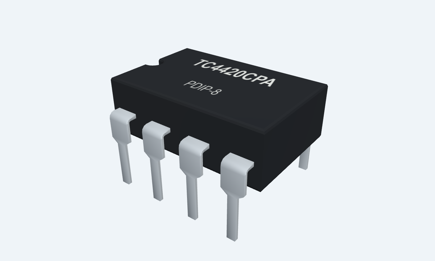
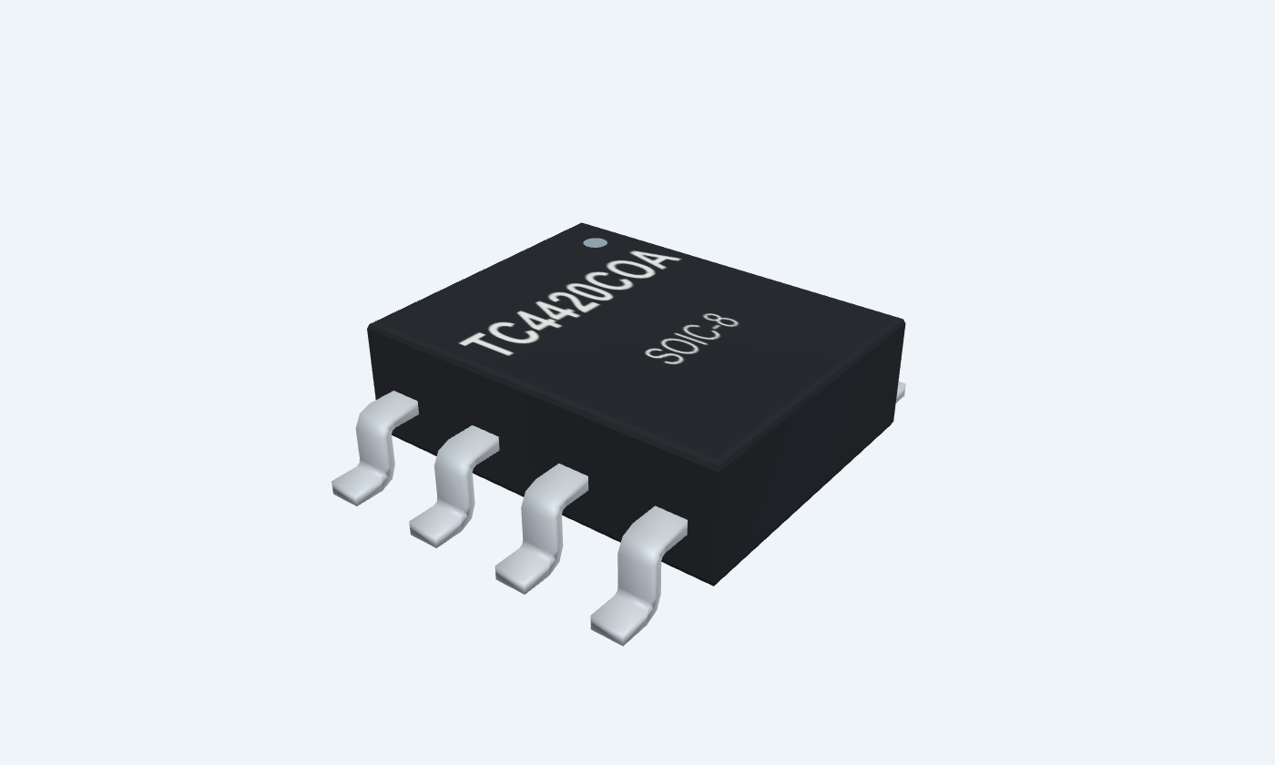
Charge and discharge a MOSFET gate with a dedicated driver.
TC4420 is a non-inverting gate driver that converts a logic signal into short, high-current pulses for charging and discharging a MOSFET gate. It is a driver stage, not a MOSFET power switch or an oscillator. The commercial DIP8 and SOIC8 versions share the same physical pin functions. Both VDD pins, both ground pins and both output pins must be connected. The duplicated contacts carry fast transient currents and are not optional alternatives. Local bypassing and a short driver-to-gate loop are essential to avoid ringing and supply disturbance. The example uses a 12 V driver supply, a 0–5 V PWM input and a 10 Ω gate resistor feeding a grounded-source N-channel MOSFET. A 100 kΩ gate-to-source resistor defines the off state. The 6 A figure is a peak rating under stated conditions; it is not a continuous load-current rating.
Select a pin to explore its connection
Click a lead or use the arrow keys. Top view
Driver supply
Join pin 8 to +12 V in the example; decouple locally.
Non-inverting logic input
Apply 0–5 V PWM with a common ground; use a 10 kΩ pulldown.
Unused contact
Leave unconnected.
Driver return
Join pin 5 and the MOSFET source with a short return.
Duplicated driver return
Connect together with pin 4.
Gate-drive output
Join pin 7; connect through 10 Ω to the MOSFET gate.
Duplicated gate-drive output
Connect together with pin 6.
Duplicated supply
Connect together with pin 1.
Charge and discharge a MOSFET gate with a dedicated driver.
TC4420CPA · PDIP-8
| Property | Details |
|---|---|
| Manufacturer | Microchip Technology |
| Part number | TC4420CPA |
| Package | PDIP-8 |
| Connections | 8 pins |
| Mounting | Through-hole |
| Lead pitch | 2.54 mm |
| Package code | PDIP-8 |
| Thermal reference | See operating and package limits |
TC4420 C grade
Scroll sideways to see all columns.
| Parameter | Value | Conditions / notes |
|---|---|---|
| Driver supply | 4.5–18 V | Recommended operating range |
| Ambient | 0–70°C | Selected CPA / COA |
| Guaranteed HIGH input | At least 2.4 V | DC characteristic |
| Guaranteed LOW input | At most 0.8 V | DC characteristic |
| Input current | −10 to +10 µA | 0 V ≤ VIN ≤ VDD |
| Input-to-output function | Non-inverting | TC4429 is the inverting alternative |
No specifications match. Try a parameter name or a unit.
Keep the input defined during startup and supply transitions.
Manufacturer test conditions
Scroll sideways to see all columns.
| Parameter | Value | Conditions / notes |
|---|---|---|
| Peak output current | 6 A typical | VDD = 18 V; not continuous |
| Output resistance HIGH | 2.1 Ω typical; 2.8 Ω max | 18 V; 10 mA |
| Output resistance LOW | 1.5 Ω typical; 2.5 Ω max | 18 V; 10 mA |
| Rise / fall time | 25 ns typical; 35 ns max | 2500 pF load; Figure 4-1 |
| Propagation delay | 55 ns typical; 75 ns max | Figure 4-1 |
| Supply current, input HIGH | 0.45 mA typical; 1.5 mA max | VIN = 3 V, static |
| Supply current, input LOW | 55 µA typical; 150 µA max | VIN = 0 V, static |
No specifications match. Try a parameter name or a unit.
Actual gate current is limited by driver resistance, external resistor, wiring and gate voltage.
12 V driver, 5 V logic
Scroll sideways to see all columns.
| Parameter | Value | Conditions / notes |
|---|---|---|
| Supply contacts | VDD1 and VDD8 together | 100 nF + 1 µF local bypass to GND4/5 |
| Output contacts | OUTPUT6 and OUTPUT7 together | 10 Ω series gate resistor |
| MOSFET source | GND | Use a suitable N-channel device and separate load-current routing |
| Gate pulldown | 100 kΩ | Gate to source |
| Logic pulldown | 10 kΩ | INPUT2 to GND |
| Example gate-charge budget | Qg = 20 nC, f = 20 kHz | Average charge current Qg × f = 0.4 mA |
| Gate-charge power | Qg × VDD × f = 4.8 mW | Illustrative, excludes driver static and crossover losses |
No specifications match. Try a parameter name or a unit.
Gate charge is a selected MOSFET parameter, not a TC4420 specification.
TC4420CPA · PDIP-8
Scroll sideways to see all columns.
| Parameter | Value | Conditions / notes |
|---|---|---|
| Pitch | 2.54 mm | Through-hole |
| Supply absolute maximum | 20 V | Stress ceiling |
| Power at TA ≤70°C | 730 mW PDIP; 470 mW SOIC | Derate and check actual mounting |
| Duplicate pins | All must be connected | Supply, ground and output pairs |
| Inductive load | Requires an appropriate flyback/clamp network | The shown teaching load is resistive |
No specifications match. Try a parameter name or a unit.
Do not route continuous load current through the driver output; it drives the gate.
Physical package contacts
Scroll sideways to see all columns.
| Parameter | Value | Conditions / notes |
|---|---|---|
| 1 · VDD | Driver supply | Join pin 8 to +12 V in the example; decouple locally. |
| 2 · INPUT | Non-inverting logic input | Apply 0–5 V PWM with a common ground; use a 10 kΩ pulldown. |
| 3 · NC | Unused contact | Leave unconnected. |
| 4 · GND | Driver return | Join pin 5 and the MOSFET source with a short return. |
| 5 · GND | Duplicated driver return | Connect together with pin 4. |
| 6 · OUTPUT | Gate-drive output | Join pin 7; connect through 10 Ω to the MOSFET gate. |
| 7 · OUTPUT | Duplicated gate-drive output | Connect together with pin 6. |
| 8 · VDD | Duplicated supply | Connect together with pin 1. |
No specifications match. Try a parameter name or a unit.
Connect all supply and return contacts; leave only explicitly unused contacts open.
Select a pin for its function, connection guidance and electrical notes.
Follow the labeled connections and functional stages
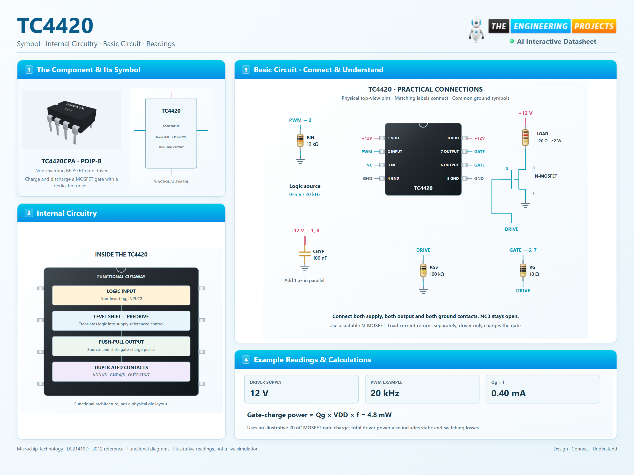
3 stages · Explore one step at a time
A valid logic input selects the output state.
The driver sources gate charge to turn a low-side MOSFET on.
It sinks gate charge to turn the MOSFET off quickly.
Physical package with colored wiring and explicit node labels.
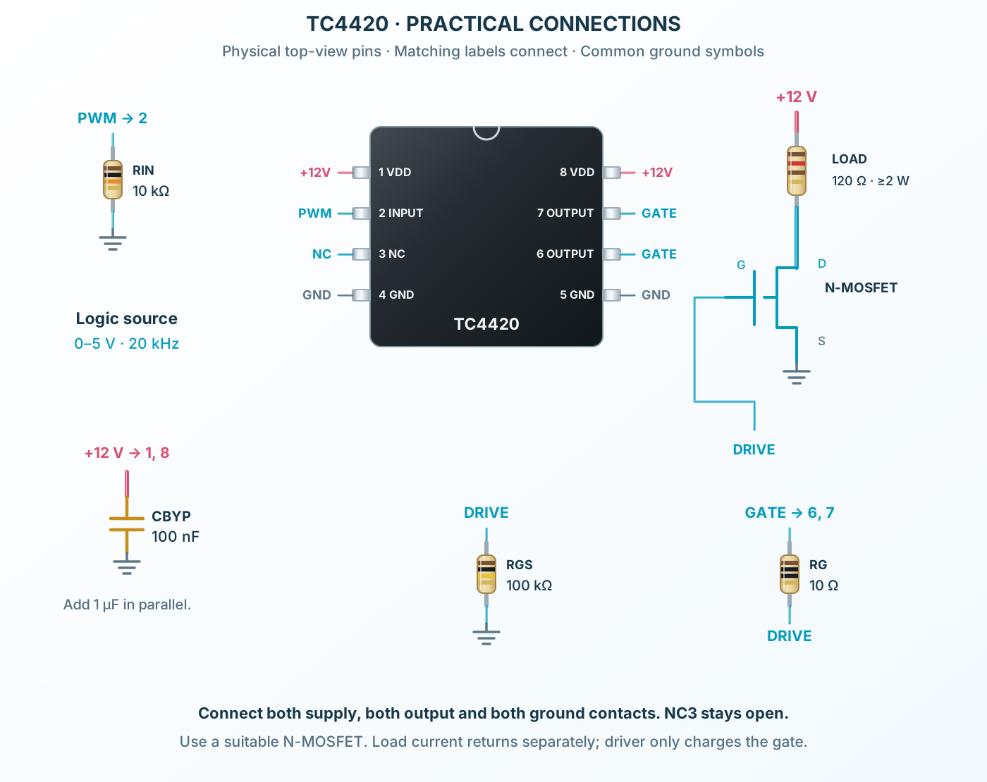
Follow the component values and pin connections
Connect every specified supply and return contact.
Fit the external components at the numbered pins shown.
Compare the nominal calculation with device and component tolerances.
Compact functional stages inside the IC body.
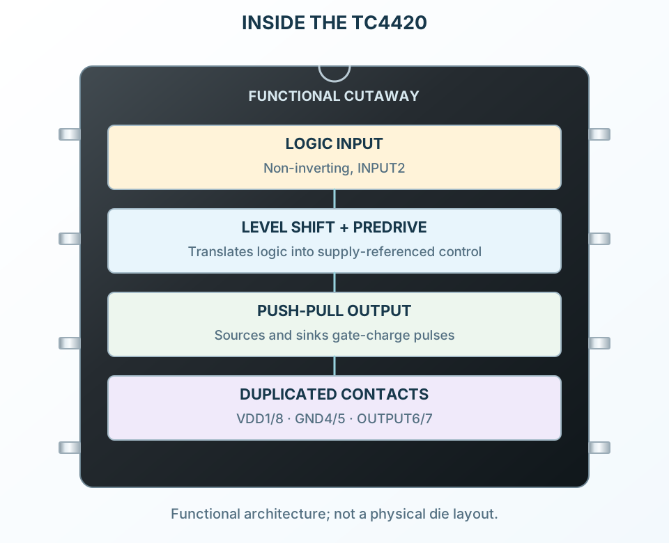
Select a stage to see its role and connections
A valid logic input selects the output state.
The driver sources gate charge to turn a low-side MOSFET on.
It sinks gate charge to turn the MOSFET off quickly.
Signal names, electrical functions and connection guidance
Scroll within the table to see all columns and rows.
| Pin | Signal | Type | Function & connection |
|---|---|---|---|
| VDD | Supply | Driver supplyConnection guidanceJoin pin 8 to +12 V in the example; decouple locally. | |
| INPUT | Input / control | Non-inverting logic inputConnection guidanceApply 0–5 V PWM with a common ground; use a 10 kΩ pulldown. | |
| NC | No connection | Unused contactConnection guidanceLeave unconnected. | |
| GND | Supply | Driver returnConnection guidanceJoin pin 5 and the MOSFET source with a short return. | |
| GND | Supply | Duplicated driver returnConnection guidanceConnect together with pin 4. | |
| OUTPUT | Output | Gate-drive outputConnection guidanceJoin pin 7; connect through 10 Ω to the MOSFET gate. | |
| OUTPUT | Output | Duplicated gate-drive outputConnection guidanceConnect together with pin 6. | |
| VDD | Supply | Duplicated supplyConnection guidanceConnect together with pin 1. |
No pins match these filters. Try another signal name or reset the filters.
TC4420 C grade
Scroll within the table to see all columns and rows.
| Parameter | Value | Conditions / notes |
|---|---|---|
| Driver supply | 4.5–18 V | Recommended operating range |
| Ambient | 0–70°C | Selected CPA / COA |
| Guaranteed HIGH input | At least 2.4 V | DC characteristic |
| Guaranteed LOW input | At most 0.8 V | DC characteristic |
| Input current | −10 to +10 µA | 0 V ≤ VIN ≤ VDD |
| Input-to-output function | Non-inverting | TC4429 is the inverting alternative |
No specifications match. Try a parameter name or a unit.
Keep the input defined during startup and supply transitions.
Manufacturer test conditions
Scroll within the table to see all columns and rows.
| Parameter | Value | Conditions / notes |
|---|---|---|
| Peak output current | 6 A typical | VDD = 18 V; not continuous |
| Output resistance HIGH | 2.1 Ω typical; 2.8 Ω max | 18 V; 10 mA |
| Output resistance LOW | 1.5 Ω typical; 2.5 Ω max | 18 V; 10 mA |
| Rise / fall time | 25 ns typical; 35 ns max | 2500 pF load; Figure 4-1 |
| Propagation delay | 55 ns typical; 75 ns max | Figure 4-1 |
| Supply current, input HIGH | 0.45 mA typical; 1.5 mA max | VIN = 3 V, static |
| Supply current, input LOW | 55 µA typical; 150 µA max | VIN = 0 V, static |
No specifications match. Try a parameter name or a unit.
Actual gate current is limited by driver resistance, external resistor, wiring and gate voltage.
12 V driver, 5 V logic
Scroll within the table to see all columns and rows.
| Parameter | Value | Conditions / notes |
|---|---|---|
| Supply contacts | VDD1 and VDD8 together | 100 nF + 1 µF local bypass to GND4/5 |
| Output contacts | OUTPUT6 and OUTPUT7 together | 10 Ω series gate resistor |
| MOSFET source | GND | Use a suitable N-channel device and separate load-current routing |
| Gate pulldown | 100 kΩ | Gate to source |
| Logic pulldown | 10 kΩ | INPUT2 to GND |
| Example gate-charge budget | Qg = 20 nC, f = 20 kHz | Average charge current Qg × f = 0.4 mA |
| Gate-charge power | Qg × VDD × f = 4.8 mW | Illustrative, excludes driver static and crossover losses |
No specifications match. Try a parameter name or a unit.
Gate charge is a selected MOSFET parameter, not a TC4420 specification.
TC4420CPA · PDIP-8
Scroll within the table to see all columns and rows.
| Parameter | Value | Conditions / notes |
|---|---|---|
| Pitch | 2.54 mm | Through-hole |
| Supply absolute maximum | 20 V | Stress ceiling |
| Power at TA ≤70°C | 730 mW PDIP; 470 mW SOIC | Derate and check actual mounting |
| Duplicate pins | All must be connected | Supply, ground and output pairs |
| Inductive load | Requires an appropriate flyback/clamp network | The shown teaching load is resistive |
No specifications match. Try a parameter name or a unit.
Do not route continuous load current through the driver output; it drives the gate.
Physical package contacts
Scroll within the table to see all columns and rows.
| Parameter | Value | Conditions / notes |
|---|---|---|
| 1 · VDD | Driver supply | Join pin 8 to +12 V in the example; decouple locally. |
| 2 · INPUT | Non-inverting logic input | Apply 0–5 V PWM with a common ground; use a 10 kΩ pulldown. |
| 3 · NC | Unused contact | Leave unconnected. |
| 4 · GND | Driver return | Join pin 5 and the MOSFET source with a short return. |
| 5 · GND | Duplicated driver return | Connect together with pin 4. |
| 6 · OUTPUT | Gate-drive output | Join pin 7; connect through 10 Ω to the MOSFET gate. |
| 7 · OUTPUT | Duplicated gate-drive output | Connect together with pin 6. |
| 8 · VDD | Duplicated supply | Connect together with pin 1. |
No specifications match. Try a parameter name or a unit.
Connect all supply and return contacts; leave only explicitly unused contacts open.
No matching rowsTry a pin name, parameter, unit or test condition, or reset the filters.
Use the reviewed basic circuit as a starting point, then verify load and temperature limits.
Manufacturer application guideCompare the internal functional blocks with the external connections.
Manufacturer application guideChoose the correct package and check the downloaded footprint before manufacture.
Manufacturer application guideFind TC4420 in the Components Library to place its schematic symbol and connect its pins.
Reference page · circuit simulation model not yet availableOpen ProTech