TL072Dual FET-input operational amplifier
Two high-impedance analog channels in one compact IC.
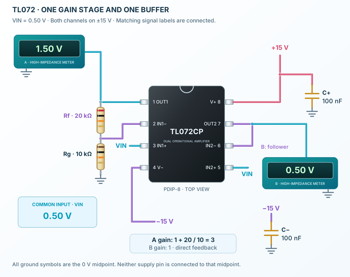
TL072 integrates two FET-input operational amplifiers. Each channel compares a pair of input voltages and uses external negative feedback to control its gain. The physical example uses channel A as a gain-of-three amplifier and channel B as a voltage follower. A shared 0.50 V input gives ideal outputs of 1.50 V and 0.50 V from a ±15 V supply. This page follows TI’s July 2025 reference for the C-grade P and D packages. Its revised P/D specifications differ from the legacy PS package; the manufacturer’s package-specific columns are kept separate.
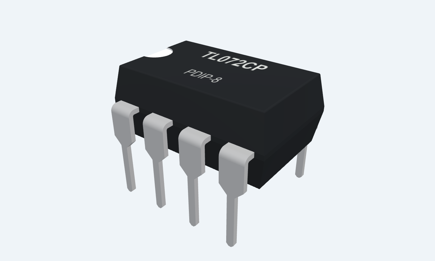
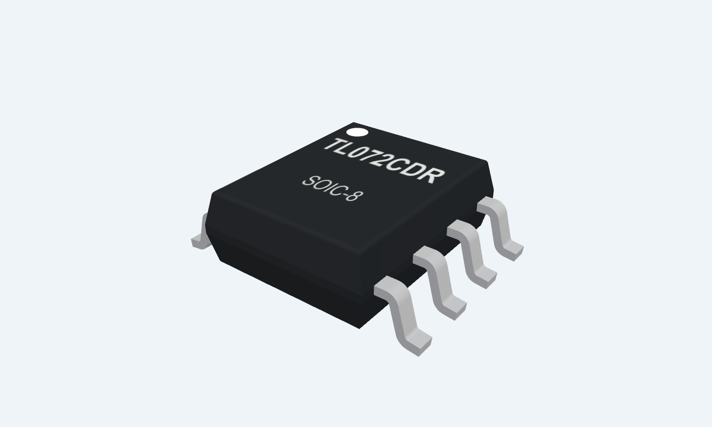

Analog outputsAnalog inputsShared supply rails
TL072CPPDIP-8Top view
TL072CDRSOIC-8Top view
Click a lead or use the arrow keys. Top view
PIN 1 · Analog outputs
Analog outputOUT1
Function
Channel A output.
How to connect
Return to IN1− through 20 kΩ; connect a high-impedance meter.
PIN 2 · Analog inputs
Inverting inputIN1−
Function
Channel A negative-feedback node.
How to connect
Join 20 kΩ from OUT1 and 10 kΩ to signal ground.
PIN 3 · Analog inputs
Non-inverting inputIN1+
Function
Channel A signal input.
How to connect
Apply VIN = 0.50 V relative to the 0 V midpoint.
PIN 4 · Shared supply rails
Negative supplyV−
Function
Negative rail shared by both amplifiers.
How to connect
Connect −15 V; bypass locally to 0 V with 100 nF.
PIN 5 · Analog inputs
Non-inverting inputIN2+
Function
Channel B signal input.
How to connect
Connect to the same VIN in the illustrated follower.
PIN 6 · Analog inputs
Inverting inputIN2−
Function
Channel B feedback input.
How to connect
Connect directly to OUT2 pin 7.
PIN 7 · Analog outputs
Analog outputOUT2
Function
Channel B output.
How to connect
Connect to IN2−; leave unloaded or use a high-impedance instrument.
PIN 8 · Shared supply rails
Positive supplyV+
Function
Positive rail shared by both amplifiers.
How to connect
Connect +15 V; bypass locally to 0 V with 100 nF.
At a glance
Dual FET-input operational amplifier
High input impedance suits voltage buffering and active filters. Each channel needs its own negative-feedback path.
4.5–40 V · TI P/D packages, Rev WSupply span
5.25 MHz · P/D packagesTypical bandwidth
0–70 °CC-grade ambient
20 V/µs · specified testTypical slew rate
Operating profile
TL072CP
Operating conditions
Key parameters and their test conditions
- Total supply span
- 4.5–40 VConditions / notes: V+ minus V−; Rev W, all except NS/PS/M
- Ambient temperature
- 0 to +70°CConditions / notes: TL072C grade
- Recommended input range
- V− + 4 V to V+ + 0.1 VConditions / notes: Observe supply and signal restrictions
- Example supply
- +15 V / −15 VConditions / notes: 0 V is the midpoint
- Legacy PS package
- 10–30 V total supplyConditions / notes: Different column; not the package illustrated here
Package details
Follows the selected physical package
- Manufacturer
- Texas Instruments
- Part number
- TL072CP
- Package
- PDIP-8
- Connections
- 8 pins
- Mounting
- Through-hole
- Lead pitch
- 2.54 mm
- Package code
- dip
- Thermal reference
- Board and package dependent; see manufacturer data
Connections by function
Select a pin to open its function, electrical notes and wiring guidance.
Analog outputs2 pins
Analog inputs4 pins
Shared supply rails2 pins
Analog outputs2 pins
Analog inputs4 pins
Shared supply rails2 pins
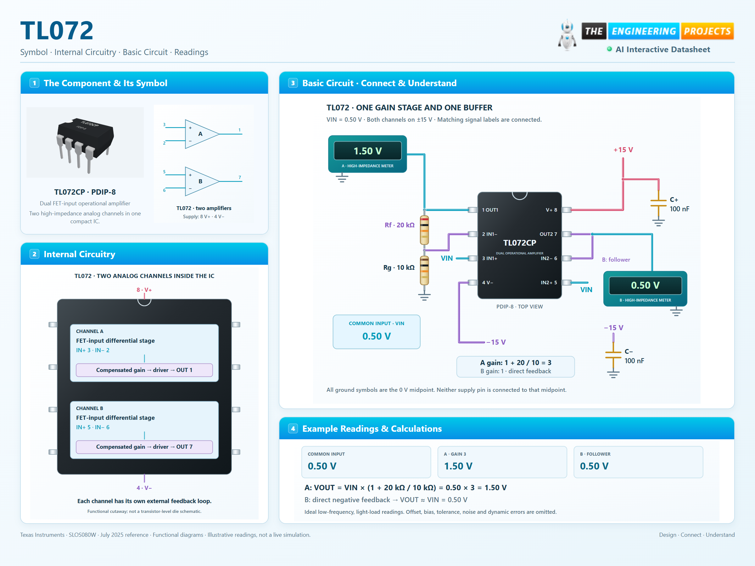
Compare each input pair
The FET input stage draws very little bias current at room temperature. Source resistance, board leakage and temperature still affect the input error.
Set two different gains
Channel A uses 20 kΩ feedback and 10 kΩ to the 0 V midpoint, giving a gain of three. Channel B directly feeds its output back to its negative input, giving unity gain.
Check headroom and speed
With a 0.50 V input, the ideal outputs are 1.50 V and 0.50 V. Real output also depends on input offset, resistor accuracy, loading, noise and signal frequency.
Both channels share the supply rails but have independent feedback paths. The diagram shows a low-frequency, light-load example; use the specified limits for your actual circuit.
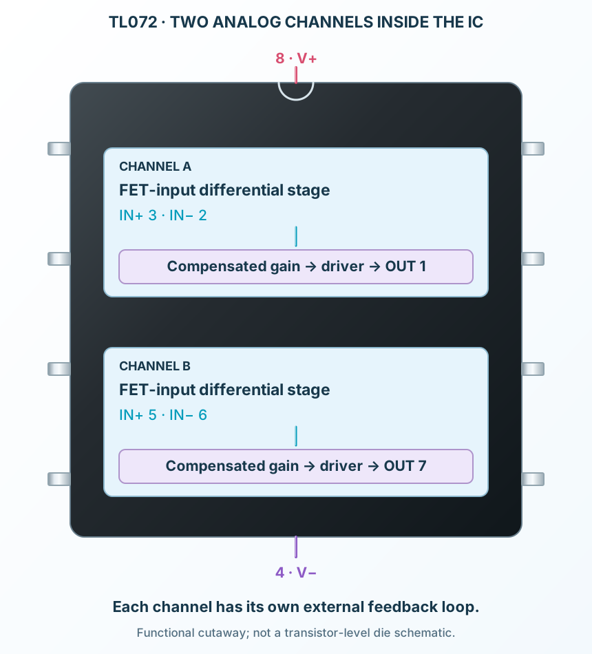
Pin reference
Select a pin to explore its function and connection.
8 pins
| Pin | Signal | Type | Function |
|---|---|---|---|
| OUT1 | Analog output | Channel A output. | |
| IN1− | Inverting input | Channel A negative-feedback node. | |
| IN1+ | Non-inverting input | Channel A signal input. | |
| V− | Negative supply | Negative rail shared by both amplifiers. | |
| IN2+ | Non-inverting input | Channel B signal input. | |
| IN2− | Inverting input | Channel B feedback input. | |
| OUT2 | Analog output | Channel B output. | |
| V+ | Positive supply | Positive rail shared by both amplifiers. |
No pins match. Try a signal name or choose All pins.
Operating conditions
TI TL072C · P/D package columns
Manufacturer specifications 5 parameters
| Parameter | Value | Conditions / notes |
|---|---|---|
| Total supply span | 4.5–40 V | V+ minus V−; Rev W, all except NS/PS/M |
| Ambient temperature | 0 to +70°C | TL072C grade |
| Recommended input range | V− + 4 V to V+ + 0.1 V | Observe supply and signal restrictions |
| Example supply | +15 V / −15 V | 0 V is the midpoint |
| Legacy PS package | 10–30 V total supply | Different column; not the package illustrated here |
No specifications match. Try a parameter name or a unit.
Values follow the stated revision and package. Do not apply current P/D limits to an unidentified older die.
DC characteristics
±15 V · 25°C unless stated
Manufacturer specifications 7 parameters
| Parameter | Value | Conditions / notes |
|---|---|---|
| Input offset voltage | 3 mV typical; 10 mV maximum | TL072C; RS = 50 Ω |
| Input offset, full temperature | 13 mV maximum | 0–70°C |
| Input bias current | 65 pA typical; 200 pA maximum | 7 nA maximum over temperature |
| Input offset current | 5 pA typical; 100 pA maximum | 10 nA maximum over temperature |
| Supply current per amplifier | 1.4 mA typical; 2.5 mA maximum | No load; output at 0 V |
| Common-mode range | ±11 V minimum; −12 to +15 V typical | ±15 V test supply |
| Output swing | ±12 V minimum; ±13.5 V typical | RL = 10 kΩ |
No specifications match. Try a parameter name or a unit.
Typical values describe representative devices; use specified limits for error budgets.
Dynamic characteristics
TI Rev W · P/D packages
Manufacturer specifications 5 parameters
| Parameter | Value | Conditions / notes |
|---|---|---|
| Gain-bandwidth product | 5.25 MHz typical | P/D package column |
| Slew rate | 8 V/µs minimum; 20 V/µs typical | 10 V input; CL = 100 pF; RL = 2 kΩ |
| Input voltage noise at 1 kHz | 37 nV/√Hz typical | All except PS/NS/M |
| Input voltage noise at 10 kHz | 21 nV/√Hz typical | P/D package column |
| Phase margin | 56° typical | Gain +1; RL = 10 kΩ; CL = 20 pF |
No specifications match. Try a parameter name or a unit.
Bandwidth, slew rate and settling behavior are different limits; check all three for a changing signal.
Two-channel amplifier example
±15 V rails · 0 V signal reference
Manufacturer specifications 7 parameters
| Parameter | Value | Conditions / notes |
|---|---|---|
| Input VIN | 0.50 V | Pins 3 and 5; common signal ground |
| Channel A feedback | 20 kΩ | OUT1 pin 1 to IN1− pin 2 |
| Channel A ground resistor | 10 kΩ | IN1− pin 2 to 0 V |
| Channel A ideal output | 1.50 V | 0.50 × (1 + 20 / 10) |
| Channel B feedback | Direct connection | OUT2 pin 7 to IN2− pin 6 |
| Channel B ideal output | 0.50 V | Unity-gain follower |
| Bypass capacitors | 100 nF per rail | Each supply rail to the 0 V midpoint |
No specifications match. Try a parameter name or a unit.
The 0 V reference is not the negative supply pin. Keep both rail-bypass loops short.
Physical pin reference
TL072CP · PDIP-8
Manufacturer specifications 5 parameters
| Parameter | Value | Conditions / notes |
|---|---|---|
| Lead pitch | 2.54 mm | Through-hole |
| Channel A | OUT1 1; IN1− 2; IN1+ 3 | Independent feedback loop |
| Channel B | IN2+ 5; IN2− 6; OUT2 7 | Independent feedback loop |
| Supply | V− 4; V+ 8 | Shared by both channels |
| Package orientation | Top view; pin 1 at the marker | Counterclockwise numbering |
No specifications match. Try a parameter name or a unit.
This dual-amplifier pinout differs from single amplifiers such as TL081 or LM741.
High-impedance buffers
Buffer suitable high-resistance signal sources with attention to input leakage and common-mode range.
Manufacturer application guideActive filters
Use separate feedback networks to build two filter stages, or a filter and an output buffer.
Manufacturer application guideAudio conditioning
Build gain or mixing stages with appropriate coupling, supply decoupling and load headroom.
Manufacturer application guideTake it into ProTech
Find TL072 in the Components Library to place its schematic symbol and connect its pins.
Reference page · circuit simulation model not yet availableOpen ProTech