Real View
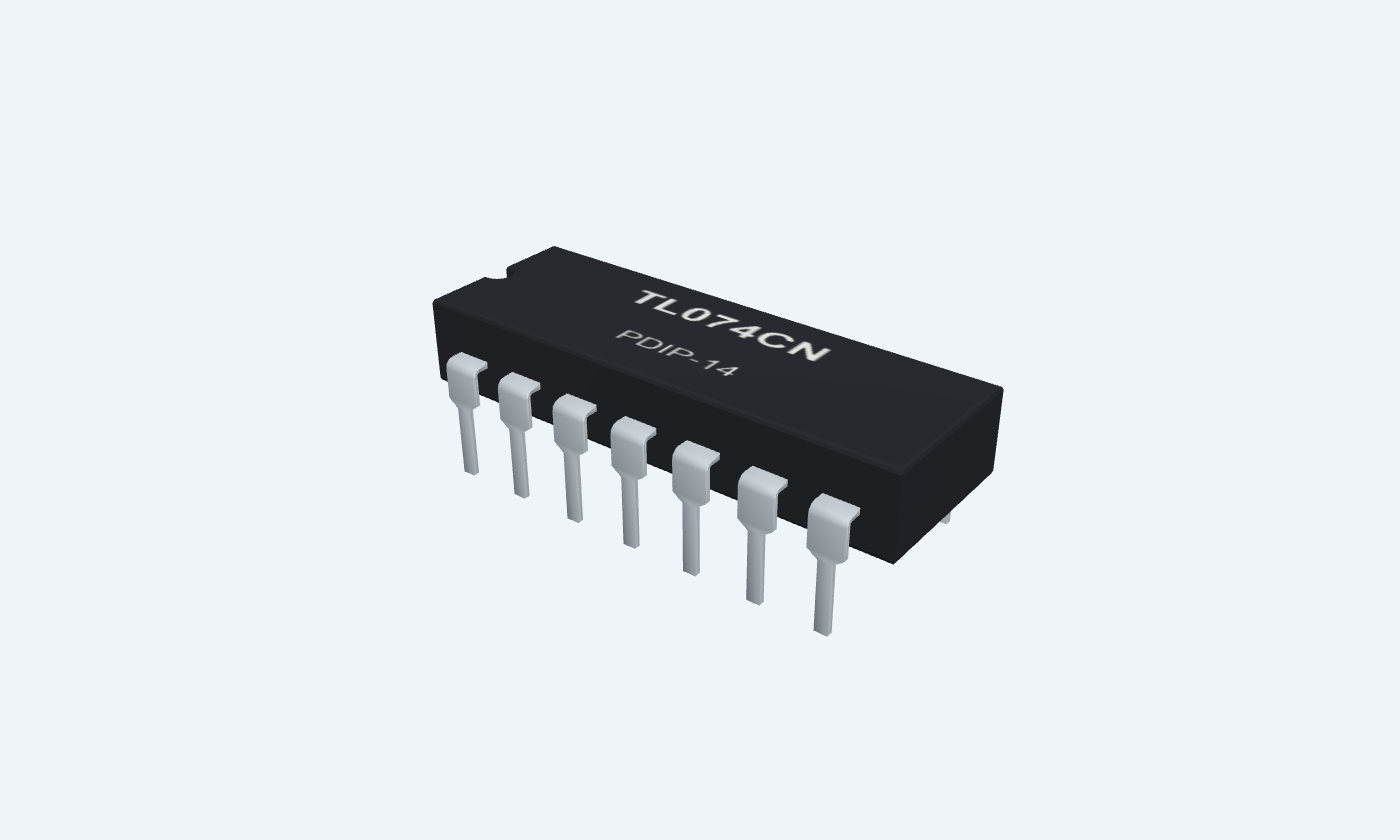
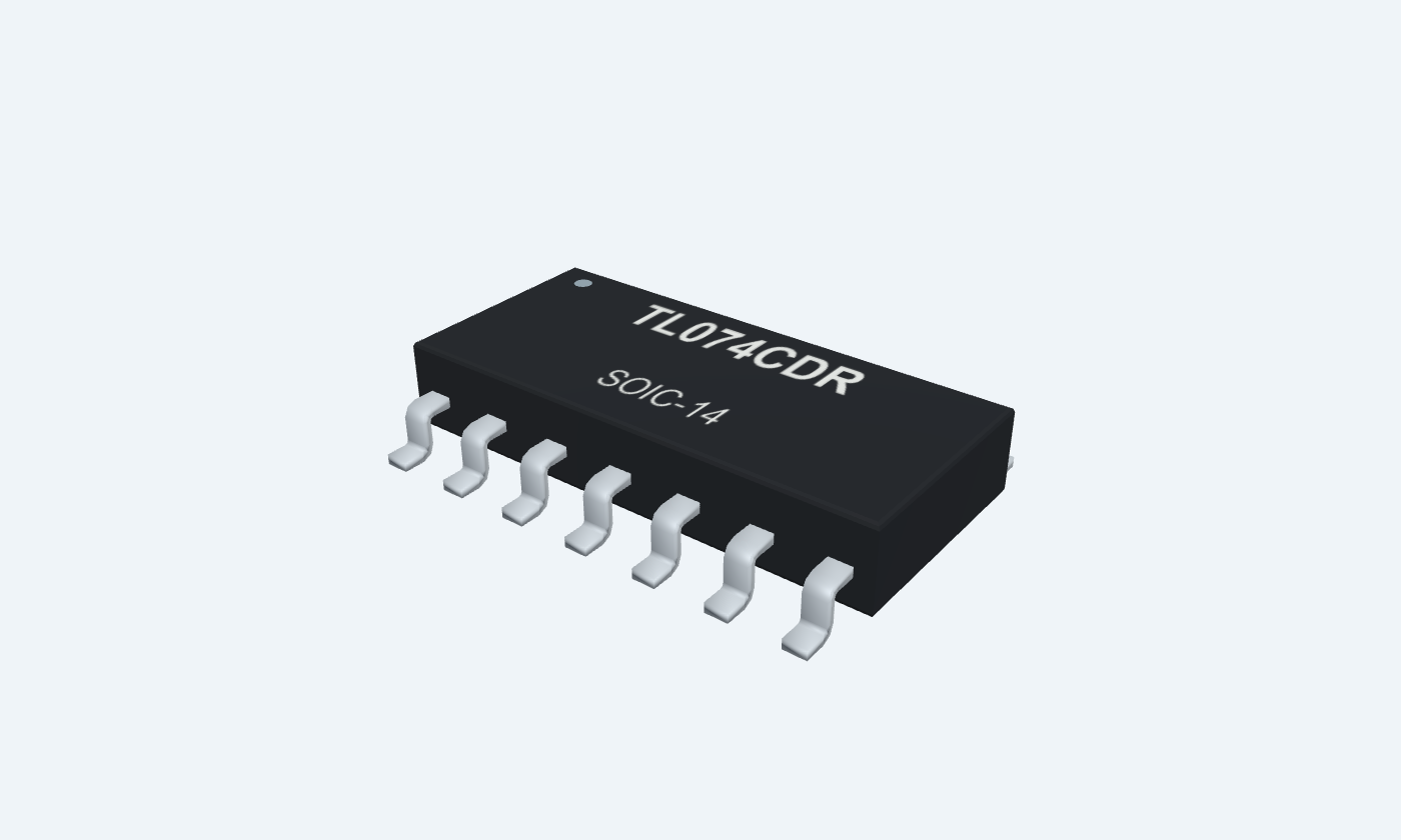
Four low-input-current channels for analog signal paths.
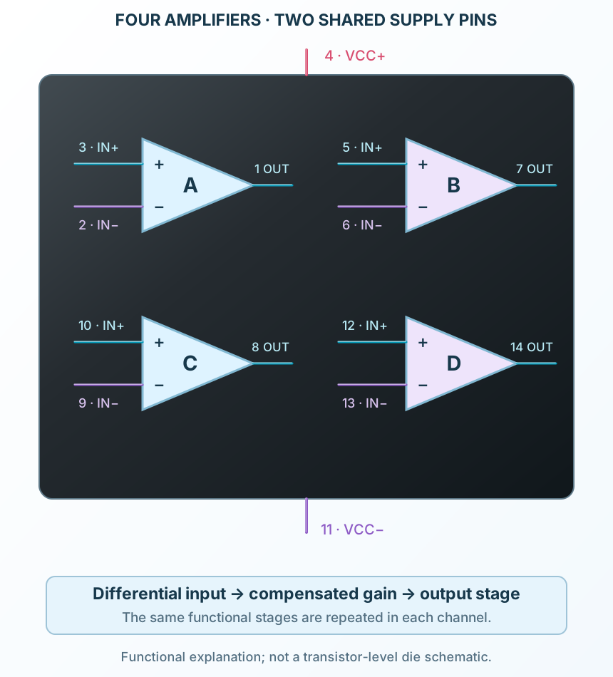
TL074 contains four FET-input operational amplifiers in a fourteen-pin package. Separate input pairs and outputs allow four feedback circuits to share one pair of supply rails. Its low input current suits analog buffers, active filters and signal-conditioning stages. The selected commercial parts are TL074CN in PDIP-14 and TL074CDR in SOIC-14, rated for 0 to 70°C. TI identifies both legacy SFAB and newer RFB silicon under non-H part numbers. This page labels its electrical data as the original-die tables in revision W; verify the shipment’s CSO identifier before using revision-specific limits. The example uses ±15 V rails, a 0 V signal midpoint and 0.40 V input. Channel A has a gain of four and ideally produces 1.60 V; the other three channels are defined, lightly loaded followers. Input/output headroom, offset, bias current and signal speed limit real accuracy.
Select a pin to explore its connection
Click a lead or use the arrow keys. Top view
Channel A output.
Connect the 30 kΩ feedback resistor and high-impedance meter.
Output swing requires supply headroom.
Channel A negative-feedback node.
Join 30 kΩ from OUTA and 10 kΩ to the 0 V midpoint.
Channel A positive input.
Connect to the common 0.40 V input in the example.
Stay within the specified input common-mode range.
Positive rail shared by four channels.
Connect +15 V; bypass locally to 0 V with 100 nF.
Channel B positive input.
Connect to the common 0.40 V input in the example.
Stay within the specified input common-mode range.
Channel B negative-feedback node.
Join directly to OUTB for a follower.
Channel B output.
Connect to its own negative input; no external load in this example.
Output swing requires supply headroom.
Channel C output.
Connect to its own negative input; no external load in this example.
Output swing requires supply headroom.
Channel C negative-feedback node.
Join directly to OUTC for a follower.
Channel C positive input.
Connect to the common 0.40 V input in the example.
Stay within the specified input common-mode range.
Negative rail shared by four channels.
Connect −15 V; bypass locally to 0 V with 100 nF.
This is not signal ground in the split-supply example.
Channel D positive input.
Connect to the common 0.40 V input in the example.
Stay within the specified input common-mode range.
Channel D negative-feedback node.
Join directly to OUTD for a follower.
Channel D output.
Connect to its own negative input; no external load in this example.
Output swing requires supply headroom.
Keep every amplifier input defined. The illustrated followers close their own feedback loops; none of the spare channels is left floating.
TL074CN · PDIP-14
| Property | Details |
|---|---|
| Manufacturer | Texas Instruments |
| Part number | TL074CN |
| Package | PDIP-14 |
| Connections | 14 pins |
| Mounting | Through-hole |
| Lead pitch | 2.54 mm |
| Package code | dip |
| Thermal reference | Board and package dependent; see manufacturer data |
TI revision W · manufacturer ordering data
Scroll sideways to see all columns.
| Parameter | Value | Conditions / notes |
|---|---|---|
| Through-hole order | TL074CN | PDIP-14 N; commercial 0–70°C |
| SMD order | TL074CDR | SOIC-14 D; commercial 0–70°C |
| Legacy flow | CSO SFAB | Use sections 5.8, 5.9 and 5.11 |
| Latest flow | CSO RFB | Use sections 5.7 and 5.10 |
| Non-H, non-M orders | May use either flow | Confirm shipment identity; suffix alone is insufficient |
| Page electrical reference | Original-die tables 5.8 and 5.9 | No TL074H accuracy or temperature claims substituted |
No specifications match. Try a parameter name or a unit.
Use the manufacturer PDF and shipment label together.
Selected N/D package; original-table characterization
Scroll sideways to see all columns.
| Parameter | Value | Conditions / notes |
|---|---|---|
| Illustrated split rails | +15 V and −15 V | 30 V total supply span |
| Revision-W recommended span | 4.5–40 V for the all-other-devices category | NS/PS and M exceptions: 10–30 V; verify die-specific applicability |
| Revision-W recommended input | VCC−+4 V to VCC++0.1 V | All-other-devices category; do not treat as rail-to-rail output |
| C-grade ambient | 0 to70°C | Not I, M or H temperature limits |
| Common-mode at ±15 V | ±11 V minimum; −12 to+15 V typical | Original-die electrical table |
| Output swing, RL10 kΩ | ±12 V minimum; ±13.5 V typical | At ±15 V; ±12 V minimum over temperature |
| Output swing, RL≥2 kΩ | ±10 V minimum | Output loading reduces swing |
No specifications match. Try a parameter name or a unit.
The ±15 V example has generous input and output headroom.
C-grade · ±15 V ·25°C unless stated
Scroll sideways to see all columns.
| Parameter | Value | Conditions / notes |
|---|---|---|
| Input offset voltage | 3 mV typical; 10 mV maximum | 13 mV maximum over full temperature; RS50 Ω |
| Input offset drift | ±18 µV/°C typical | Full-temperature characterization |
| Input bias current | 65 pA typical; 200 pA maximum | 7 nA maximum over full temperature |
| Input offset current | 5 pA typical; 100 pA maximum | 10 nA maximum over full temperature for C grade |
| Quiescent current per amplifier | 1.4 mA typical; 2.5 mA maximum | No load; VO0 V; four channels total 5.6 mA typ. |
| Open-loop gain | 25 V/mV minimum; 200 V/mV typical | C grade; 15 V/mV minimum over full temperature |
| CMRR / PSRR | 70 dB minimum; 100 dB typical | C grade; source test conditions retained |
No specifications match. Try a parameter name or a unit.
Low room-temperature bias current does not imply negligible high-temperature leakage.
Revision-W tables; N/D package category
Scroll sideways to see all columns.
| Parameter | Value | Conditions / notes |
|---|---|---|
| Gain-bandwidth product | 5.25 MHz typical | All-other-devices category; NS/PS/M table entry is 3 MHz |
| Slew rate | 8 V/µs minimum; 20 V/µs typical | VI10 V, CL100 pF, RL2 kΩ; C grade |
| Input voltage noise at1 kHz | 37 nV/√Hz typical | All-other-devices category |
| Input voltage noise at10 kHz | 21 nV/√Hz typical | Noise density, not integrated RMS noise |
| Low-frequency voltage noise | 1.4 µV RMS typical | 0.1–10 Hz; all-other-devices category |
| Input current noise | 10 fA/√Hz typical | 1 kHz; RS20 Ω |
| Phase margin | 56° typical | Gain+1, RL10 kΩ, CL20 pF |
No specifications match. Try a parameter name or a unit.
These revision-W values must not be silently replaced by older family summaries or the H-die table.
Split-supply circuit with defined unused channels
Scroll sideways to see all columns.
| Parameter | Value | Conditions / notes |
|---|---|---|
| Input VIN | 0.40 V | To pins3,5,10,12; referenced to0 V |
| A feedback | 30 kΩ fromOUT1 toIN−2 | 10 kΩ fromIN−2 to0 V |
| A ideal output | 1.60 V | 0.40×(1+30/10) |
| B follower | OUT7 connected toIN−6 | Input5; ideal output0.40 V |
| C follower | OUT8 connected toIN−9 | Input10; ideal output0.40 V |
| D follower | OUT14 connected toIN−13 | Input12; ideal output0.40 V |
| Bypass | 100 nF per supply rail to0 V | Positive pin4; negative pin11 |
No specifications match. Try a parameter name or a unit.
The midpoint is not pin11. Both supplies are required for the shown circuit.
TL074CN · PDIP-14
Scroll sideways to see all columns.
| Parameter | Value | Conditions / notes |
|---|---|---|
| Lead pitch | 2.54 mm | Through-hole |
| ChannelA | 3 IN+;2 IN−;1 OUT | Independent amplifier |
| ChannelB | 5 IN+;6 IN−;7 OUT | Independent amplifier |
| ChannelC | 10 IN+;9 IN−;8 OUT | Independent amplifier |
| ChannelD | 12 IN+;13 IN−;14 OUT | Independent amplifier |
| Shared rails | 4 VCC+;11 VCC− | Top-view counterclockwise numbering |
| PCB practice | Short feedback and bypass loops | Keep output currents away from sensitive input returns |
No specifications match. Try a parameter name or a unit.
Check the exact package before manufacture.
Select a pin for its function, connection guidance and electrical notes.
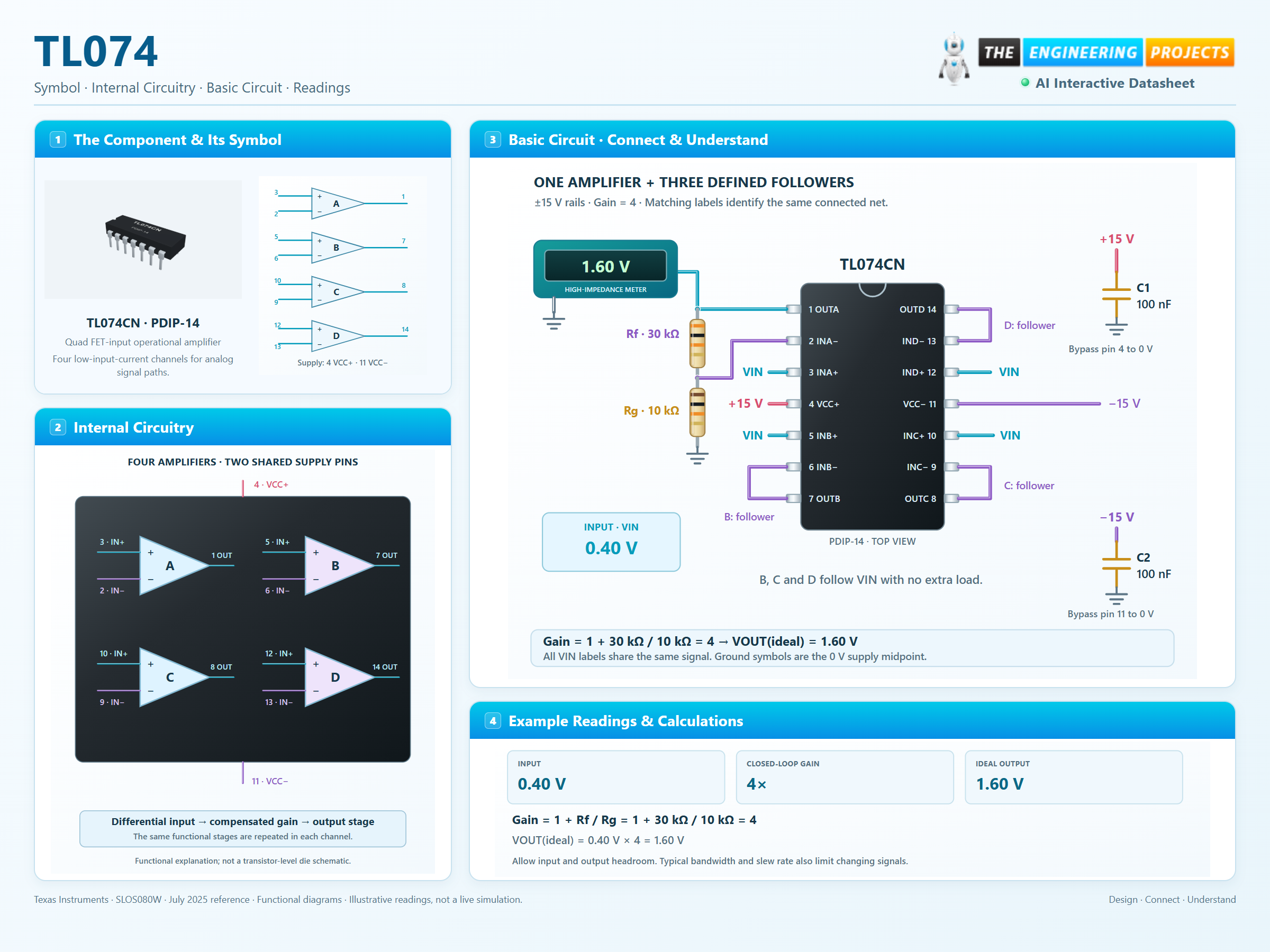
Follow the labeled connections and functional stages
3 stages · Explore one step at a time
Each input stage compares its positive input with its feedback node.
A uses 30 kΩ / 10 kΩ for gain four. B, C and D each connect output to their own negative input.
Use the 0 V supply midpoint as signal ground. Check common-mode and output headroom before increasing amplitude.
A physical fourteen-pin IC with clearly identified split supplies.
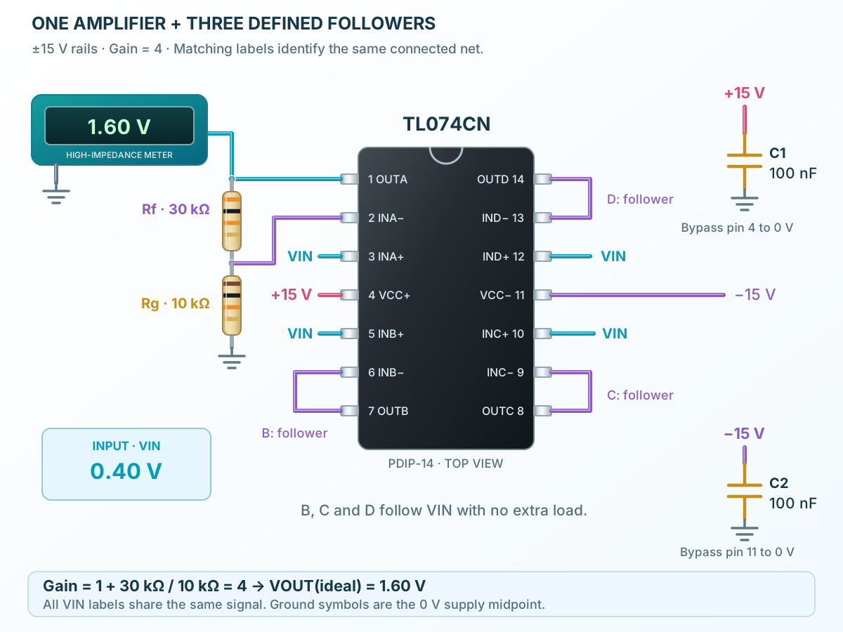
Follow the component values and pin connections
Connect+15 V to4,−15 V to11; bypass each rail to0 V.
Use30 kΩ/10 kΩ forA and direct feedback forB,C,D.
Expect1.60 V atA and0.40 V at the unloaded followers, before device error.
Four amplifier channels in a compact package cutaway.
Select a stage to see its role and connections
Each input pair senses the signal/feedback difference.
An internal gain and compensation path controls each output.
All four channels share pins4and11, while feedback remains independent.
Signal names, electrical functions and connection guidance
Scroll within the table to see all columns and rows.
| Pin | Signal | Type | Function & connection |
|---|---|---|---|
| OUTA | Analog output | Channel A output.Connection guidanceConnect the 30 kΩ feedback resistor and high-impedance meter. Output swing requires supply headroom. | |
| INA− | Inverting input | Channel A negative-feedback node.Connection guidanceJoin 30 kΩ from OUTA and 10 kΩ to the 0 V midpoint. | |
| INA+ | Non-inverting input | Channel A positive input.Connection guidanceConnect to the common 0.40 V input in the example. Stay within the specified input common-mode range. | |
| VCC+ | Positive supply | Positive rail shared by four channels.Connection guidanceConnect +15 V; bypass locally to 0 V with 100 nF. | |
| INB+ | Non-inverting input | Channel B positive input.Connection guidanceConnect to the common 0.40 V input in the example. Stay within the specified input common-mode range. | |
| INB− | Inverting input | Channel B negative-feedback node.Connection guidanceJoin directly to OUTB for a follower. | |
| OUTB | Analog output | Channel B output.Connection guidanceConnect to its own negative input; no external load in this example. Output swing requires supply headroom. | |
| OUTC | Analog output | Channel C output.Connection guidanceConnect to its own negative input; no external load in this example. Output swing requires supply headroom. | |
| INC− | Inverting input | Channel C negative-feedback node.Connection guidanceJoin directly to OUTC for a follower. | |
| INC+ | Non-inverting input | Channel C positive input.Connection guidanceConnect to the common 0.40 V input in the example. Stay within the specified input common-mode range. | |
| VCC− | Negative supply | Negative rail shared by four channels.Connection guidanceConnect −15 V; bypass locally to 0 V with 100 nF. This is not signal ground in the split-supply example. | |
| IND+ | Non-inverting input | Channel D positive input.Connection guidanceConnect to the common 0.40 V input in the example. Stay within the specified input common-mode range. | |
| IND− | Inverting input | Channel D negative-feedback node.Connection guidanceJoin directly to OUTD for a follower. | |
| OUTD | Analog output | Channel D output.Connection guidanceConnect to its own negative input; no external load in this example. Output swing requires supply headroom. |
No pins match these filters. Try another signal name or reset the filters.
TI revision W · manufacturer ordering data
Scroll within the table to see all columns and rows.
| Parameter | Value | Conditions / notes |
|---|---|---|
| Through-hole order | TL074CN | PDIP-14 N; commercial 0–70°C |
| SMD order | TL074CDR | SOIC-14 D; commercial 0–70°C |
| Legacy flow | CSO SFAB | Use sections 5.8, 5.9 and 5.11 |
| Latest flow | CSO RFB | Use sections 5.7 and 5.10 |
| Non-H, non-M orders | May use either flow | Confirm shipment identity; suffix alone is insufficient |
| Page electrical reference | Original-die tables 5.8 and 5.9 | No TL074H accuracy or temperature claims substituted |
No specifications match. Try a parameter name or a unit.
Use the manufacturer PDF and shipment label together.
Selected N/D package; original-table characterization
Scroll within the table to see all columns and rows.
| Parameter | Value | Conditions / notes |
|---|---|---|
| Illustrated split rails | +15 V and −15 V | 30 V total supply span |
| Revision-W recommended span | 4.5–40 V for the all-other-devices category | NS/PS and M exceptions: 10–30 V; verify die-specific applicability |
| Revision-W recommended input | VCC−+4 V to VCC++0.1 V | All-other-devices category; do not treat as rail-to-rail output |
| C-grade ambient | 0 to70°C | Not I, M or H temperature limits |
| Common-mode at ±15 V | ±11 V minimum; −12 to+15 V typical | Original-die electrical table |
| Output swing, RL10 kΩ | ±12 V minimum; ±13.5 V typical | At ±15 V; ±12 V minimum over temperature |
| Output swing, RL≥2 kΩ | ±10 V minimum | Output loading reduces swing |
No specifications match. Try a parameter name or a unit.
The ±15 V example has generous input and output headroom.
C-grade · ±15 V ·25°C unless stated
Scroll within the table to see all columns and rows.
| Parameter | Value | Conditions / notes |
|---|---|---|
| Input offset voltage | 3 mV typical; 10 mV maximum | 13 mV maximum over full temperature; RS50 Ω |
| Input offset drift | ±18 µV/°C typical | Full-temperature characterization |
| Input bias current | 65 pA typical; 200 pA maximum | 7 nA maximum over full temperature |
| Input offset current | 5 pA typical; 100 pA maximum | 10 nA maximum over full temperature for C grade |
| Quiescent current per amplifier | 1.4 mA typical; 2.5 mA maximum | No load; VO0 V; four channels total 5.6 mA typ. |
| Open-loop gain | 25 V/mV minimum; 200 V/mV typical | C grade; 15 V/mV minimum over full temperature |
| CMRR / PSRR | 70 dB minimum; 100 dB typical | C grade; source test conditions retained |
No specifications match. Try a parameter name or a unit.
Low room-temperature bias current does not imply negligible high-temperature leakage.
Revision-W tables; N/D package category
Scroll within the table to see all columns and rows.
| Parameter | Value | Conditions / notes |
|---|---|---|
| Gain-bandwidth product | 5.25 MHz typical | All-other-devices category; NS/PS/M table entry is 3 MHz |
| Slew rate | 8 V/µs minimum; 20 V/µs typical | VI10 V, CL100 pF, RL2 kΩ; C grade |
| Input voltage noise at1 kHz | 37 nV/√Hz typical | All-other-devices category |
| Input voltage noise at10 kHz | 21 nV/√Hz typical | Noise density, not integrated RMS noise |
| Low-frequency voltage noise | 1.4 µV RMS typical | 0.1–10 Hz; all-other-devices category |
| Input current noise | 10 fA/√Hz typical | 1 kHz; RS20 Ω |
| Phase margin | 56° typical | Gain+1, RL10 kΩ, CL20 pF |
No specifications match. Try a parameter name or a unit.
These revision-W values must not be silently replaced by older family summaries or the H-die table.
Split-supply circuit with defined unused channels
Scroll within the table to see all columns and rows.
| Parameter | Value | Conditions / notes |
|---|---|---|
| Input VIN | 0.40 V | To pins3,5,10,12; referenced to0 V |
| A feedback | 30 kΩ fromOUT1 toIN−2 | 10 kΩ fromIN−2 to0 V |
| A ideal output | 1.60 V | 0.40×(1+30/10) |
| B follower | OUT7 connected toIN−6 | Input5; ideal output0.40 V |
| C follower | OUT8 connected toIN−9 | Input10; ideal output0.40 V |
| D follower | OUT14 connected toIN−13 | Input12; ideal output0.40 V |
| Bypass | 100 nF per supply rail to0 V | Positive pin4; negative pin11 |
No specifications match. Try a parameter name or a unit.
The midpoint is not pin11. Both supplies are required for the shown circuit.
TL074CN · PDIP-14
Scroll within the table to see all columns and rows.
| Parameter | Value | Conditions / notes |
|---|---|---|
| Lead pitch | 2.54 mm | Through-hole |
| ChannelA | 3 IN+;2 IN−;1 OUT | Independent amplifier |
| ChannelB | 5 IN+;6 IN−;7 OUT | Independent amplifier |
| ChannelC | 10 IN+;9 IN−;8 OUT | Independent amplifier |
| ChannelD | 12 IN+;13 IN−;14 OUT | Independent amplifier |
| Shared rails | 4 VCC+;11 VCC− | Top-view counterclockwise numbering |
| PCB practice | Short feedback and bypass loops | Keep output currents away from sensitive input returns |
No specifications match. Try a parameter name or a unit.
Check the exact package before manufacture.
No matching rowsTry a pin name, parameter, unit or test condition, or reset the filters.
Use multiple feedback stages with adequate bandwidth and signal headroom.
Manufacturer application guideAccount for PCB leakage and temperature as well as specified input current.
Manufacturer application guideBudget noise, offset, rail swing and output loading for each channel.
Manufacturer application guideFind TL074 in the Components Library to place its schematic symbol and connect its pins.
Reference page · circuit simulation model not yet availableOpen ProTech