TLC555Low-power CMOS timer
The familiar eight-pin timer, with a low-current CMOS core.
TLC555 is a CMOS timer with the same eight-pin arrangement as the bipolar NE555. Two comparators monitor an external timing capacitor, a latch remembers the current state, and an internal discharge switch resets the capacitor for the next interval. Its high input impedance permits small timing capacitors and low-power timing networks. This page selects commercial-grade TLC555CP in PDIP-8 and TLC555CDR in SOIC-8: recommended operation is 2–15 V and 0–70°C. Industrial TLC555I has a different 3 V minimum supply. Do not transfer the C-grade low-voltage limit to every suffix. The 5 V example uses RA = 10 kΩ, RB = 68 kΩ and C = 10 µF for approximately one blink per second. A 4.7 kΩ LED resistor keeps output loading light. The interactive calculation shows ideal steady-state timing; capacitor tolerance, leakage, startup and output loading affect real measurements.
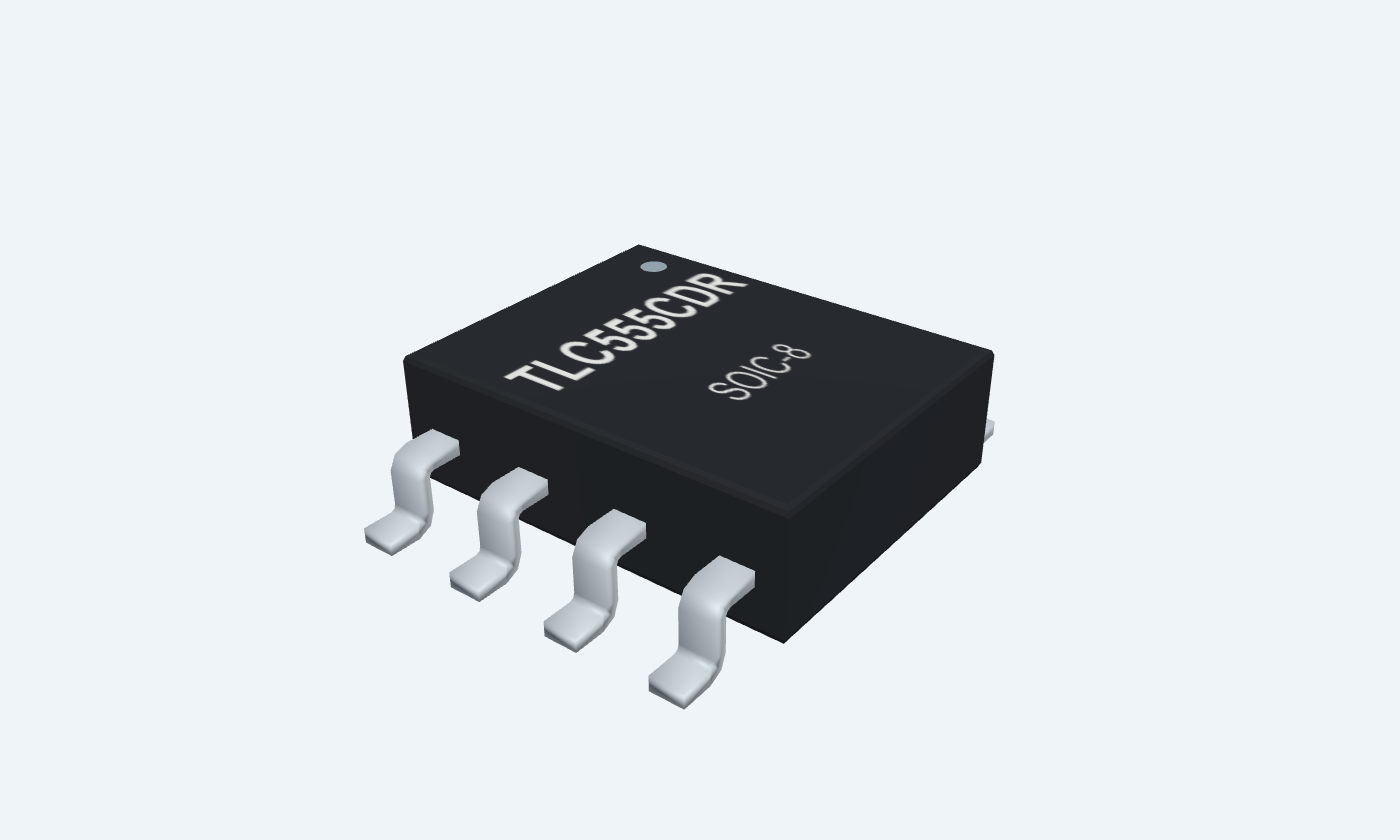

8Physical pins
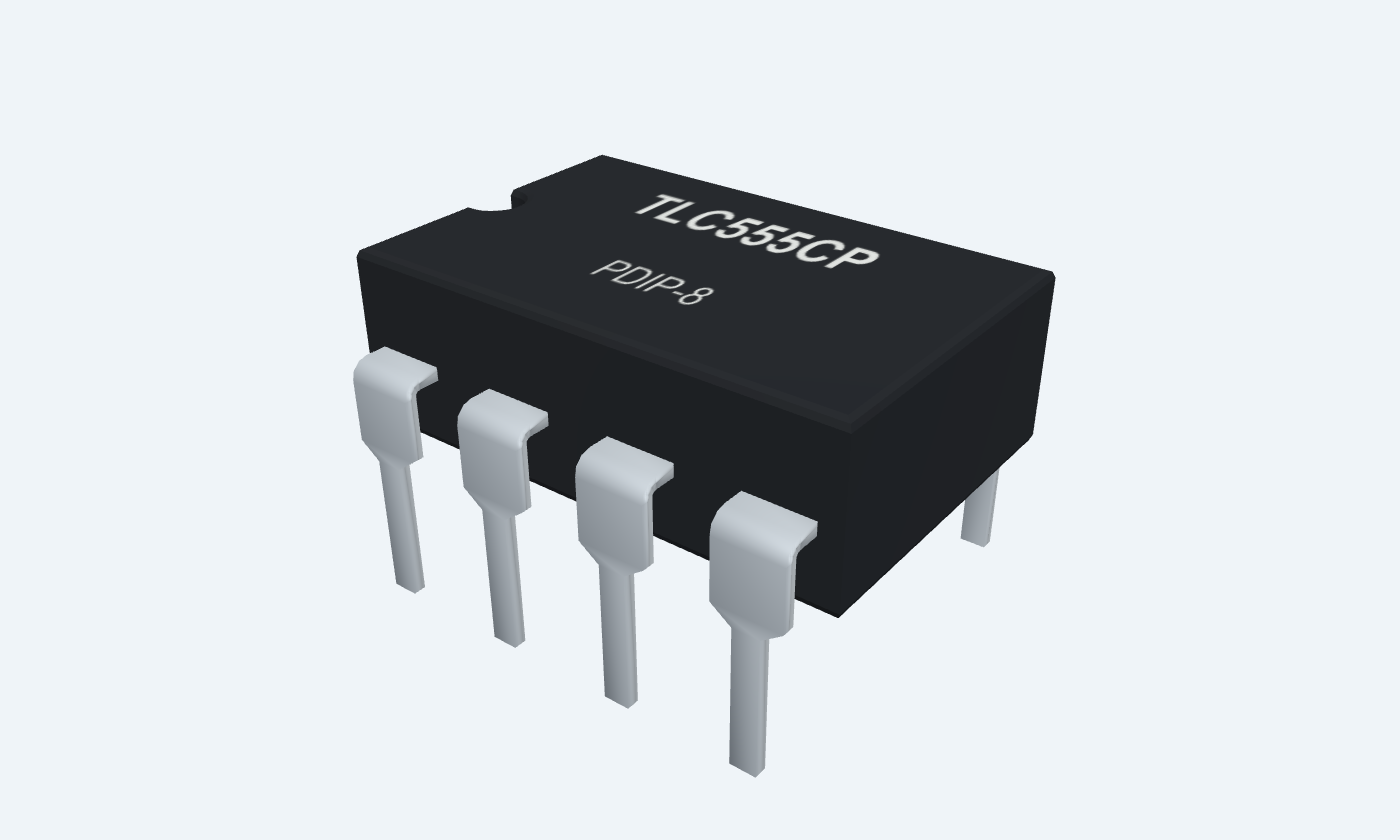
TLC555CPPDIP-8
Manufacturer-referencedTexas Instruments
Pin diagram
Select a pin to explore its connection
Highlight
TLC555CPPDIP-8Top view
TLC555CDRSOIC-8Top view
Click a lead or use the arrow keys. Top view
PIN 1 · Ground
Supply returnGND
Function
Common reference for the timer.
How to connect
Connect to circuit ground.
PIN 2 · Timing inputs
Trigger inputTRIG
Function
Below approximately one-third VDD sets the latch when RESET is inactive.
How to connect
Join THRES6 at the timing capacitor node.
Electrical note
A sustained LOW trigger can hold the output HIGH.
PIN 3 · Output and discharge
CMOS outputOUT
Function
Push-pull timing output.
How to connect
Drive an LED through 4.7 kΩ to ground.
Electrical note
Output voltage depends on load. Source capability is lower than sink capability.
PIN 4 · Reset and control
Active-LOW resetRESET
Function
Overrides the comparators, forcing OUT LOW and DISCH conducting.
How to connect
Tie to VDD for continuous oscillation.
Electrical note
Never leave RESET floating.
PIN 5 · Reset and control
Comparator referenceCONT
Function
Approximately two-thirds VDD with no external drive.
How to connect
Bypass to ground with 10 nF.
Electrical note
Changing CONT changes timing thresholds and equations.
PIN 6 · Timing inputs
Threshold inputTHRES
Function
Above CONT resets the latch when TRIG is above its lower threshold.
How to connect
Join TRIG2 at the timing capacitor node.
PIN 7 · Output and discharge
Discharge switchDISCH
Function
Provides a low-impedance path to ground while OUT is LOW.
How to connect
Connect to the RA/RB junction.
Electrical note
Not a second push-pull output.
PIN 8 · Supply
Positive supplyVDD
Function
Power for the CMOS timer.
How to connect
Apply +5 V; bypass to GND1 locally with 100 nF.
Electrical note
Selected TLC555C grade: recommended 2–15 V, 0–70°C.
Key specifications
The familiar eight-pin timer, with a low-current CMOS core.
Selected C-grade supply2–15 V recommended
Supply current180 µA typical · 5 V, 25°C
Selected ambient range0–70 °C
Package contacts8 PDIP / SOIC
Package details
TLC555CP · PDIP-8
| Property | Details |
|---|---|
| Manufacturer | Texas Instruments |
| Part number | TLC555CP |
| Package | PDIP-8 |
| Connections | 8 pins |
| Mounting | Through-hole |
| Lead pitch | 2.54 mm |
| Package code | PDIP-8 |
| Thermal reference | See operating and package limits |
Recommended operation
TLC555CP / TLC555CDR
Manufacturer specifications 5 parameters
Scroll sideways to see all columns.
| Parameter | Value | Conditions / notes |
|---|---|---|
| Supply | 2–15 V | C grade; example uses 5 V |
| Ambient | 0 to +70°C | C grade in either selected package |
| Industrial grade comparison | 3–15 V; −40 to +85°C | TLC555I, not the selected parts |
| Nominal timing window | 1/3 to 2/3 VDD | CONT unmodulated |
| Typical output capabilities | 100 mA sink; 10 mA source | Feature values, not guaranteed rail-level drive |
No specifications match. Try a parameter name or a unit.
Observe the electrical test conditions and thermal limits; output capability is asymmetric.
Five-volt electrical limits
25°C unless stated
Manufacturer specifications 8 parameters
Scroll sideways to see all columns.
| Parameter | Value | Conditions / notes |
|---|---|---|
| Supply current | 180 µA typical; 350 µA max | 5 V; expected timing configurations |
| Supply current over C-grade temperature | 500 µA max | 5 V; 0–70°C |
| Trigger threshold | 1.36–1.96 V; 1.66 V typical | 5 V, 25°C |
| Upper threshold | 2.8–3.8 V; 3.3 V typical | 5 V, 25°C |
| HIGH output | 4.8 V typical; 4.1 V minimum | Sourcing 1 mA |
| LOW output | 0.21 V typical; 0.4 V maximum | Sinking 8 mA |
| Timing-input current | 10 pA typical | 25°C; TRIG and THRES |
| Timing-input capacitance | 2.1 pF typical | Each timing input |
No specifications match. Try a parameter name or a unit.
Typical values describe characterization, not guaranteed performance for every device.
Nominal timing equations
Standard two-resistor astable
Manufacturer specifications 5 parameters
Scroll sideways to see all columns.
| Parameter | Value | Conditions / notes |
|---|---|---|
| HIGH time | ln(2) × (RA + RB) × C | Charging interval |
| LOW time | ln(2) × RB × C | Discharge interval |
| Frequency | 1 / [ln(2) × (RA + 2RB) × C] | Ω, F, seconds |
| HIGH duty cycle | (RA + RB) / (RA + 2RB) | Ordinary astable duty exceeds 50% |
| Monostable duration | Approximately 1.1 × R × C | Clean trigger must release before the interval finishes |
No specifications match. Try a parameter name or a unit.
Initial power-up timing differs from subsequent cycles. Comparator limits, leakage and component tolerance change real timing.
Low-current LED flasher
5 V · nominal 0.988 Hz
Manufacturer specifications 7 parameters
Scroll sideways to see all columns.
| Parameter | Value | Conditions / notes |
|---|---|---|
| RA / RB | 10 kΩ / 68 kΩ | RA from VDD8 to DISCH7; RB from DISCH7 to TRIG2/THRES6 |
| Timing capacitor | 10 µF | Positive at timing node, negative at ground |
| HIGH / LOW interval | 0.541 / 0.471 s | Ideal steady-state values |
| HIGH duty | 53.42% | LED anode driven through 4.7 kΩ from OUT3 |
| LED current estimate | Approximately 0.64 mA | (5−2)/4700; actual output and LED drops vary |
| RESET / CONT | 4 to VDD; 5 through 10 nF to GND | No floating controls |
| Local bypass | 100 nF | VDD8 directly to GND1 |
No specifications match. Try a parameter name or a unit.
All ground symbols are the same return. Use a driver for larger loads.
Input priority
RESET first, then trigger
Manufacturer specifications 4 parameters
Scroll sideways to see all columns.
| Parameter | Value | Conditions / notes |
|---|---|---|
| RESET LOW | OUT LOW; DISCH ON | Overrides the timing inputs |
| TRIG below lower threshold | OUT HIGH; DISCH OFF | RESET inactive |
| THRES above upper threshold | OUT LOW; DISCH ON | TRIG above lower threshold |
| Both between thresholds | Latch retains state | No new threshold crossing |
No specifications match. Try a parameter name or a unit.
The ordinary timing equations assume CONT is bypassed and RESET is HIGH.
Package and absolute limits
TLC555CP · PDIP-8
Manufacturer specifications 7 parameters
Scroll sideways to see all columns.
| Parameter | Value | Conditions / notes |
|---|---|---|
| Pitch | 2.54 mm | Through-hole |
| Absolute supply | −0.3 to +18 V | Stress rating, not the 15 V operating limit |
| Absolute input | −0.3 V to VDD | Any input |
| Absolute output/discharge sink | 150 mA | Stress limit, not recommended continuous loading |
| Absolute output source | 15 mA | Stress limit |
| Storage | −65 to +150°C | Unpowered |
| Junction-to-ambient reference | 93.1°C/W PDIP; 138.9°C/W SOIC | TI thermal test conditions; board-dependent |
No specifications match. Try a parameter name or a unit.
Do not design continuous operation at an absolute maximum.
Connections by function
Select a pin for its function, connection guidance and electrical notes.
Ground1 pin
Timing inputs2 pins
Output and discharge2 pins
Reset and control2 pins
Supply1 pin
Ground1 pin
Timing inputs2 pins
Output and discharge2 pins
Reset and control2 pins
Supply1 pin
TLC555 at a glance
Follow the labeled connections and functional stages
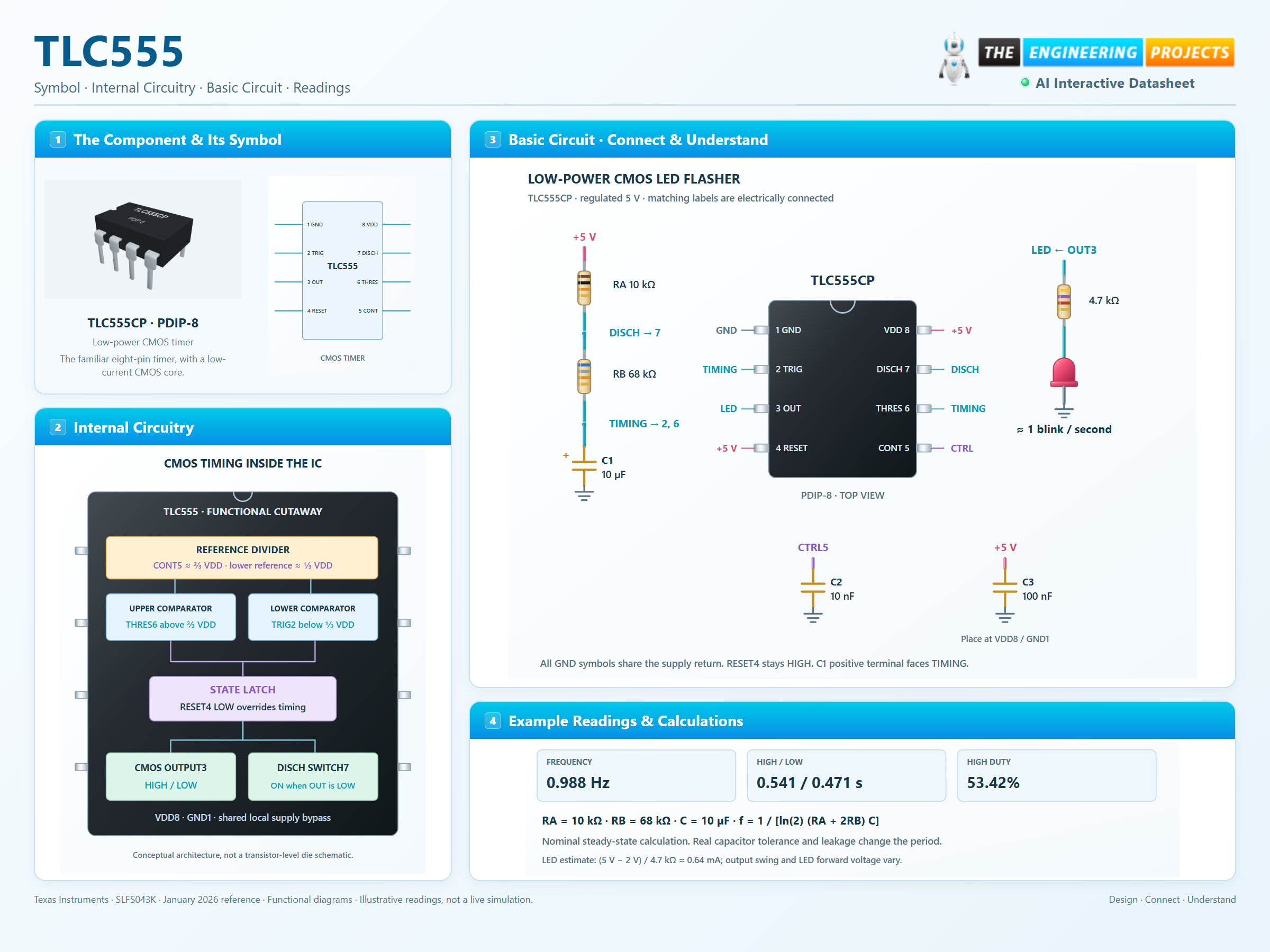
How it works
3 stages · Explore one step at a time
Charge
With DISCH open, the capacitor charges through RA plus RB until THRES crosses the upper threshold.
Discharge
The latch changes state, OUT goes LOW, and DISCH drains the capacitor through RB.
Repeat
When TRIG crosses the lower threshold, the latch sets and the next HIGH interval begins.
Step 1 of 3
Two timing networks. Two waveforms.
Adjust each channel and compare its ideal steady-state timing.
CMOS timer OUT · pin 3
——
——
Supply: 5 V. Each graph uses its own time scale. Nominal astable calculator; not a device simulation. RESET HIGH, CONT unmodulated. Tolerances, startup, leakage and output loading are not modeled.
TLC555 in a circuit
Light output loading and a shared ground return.
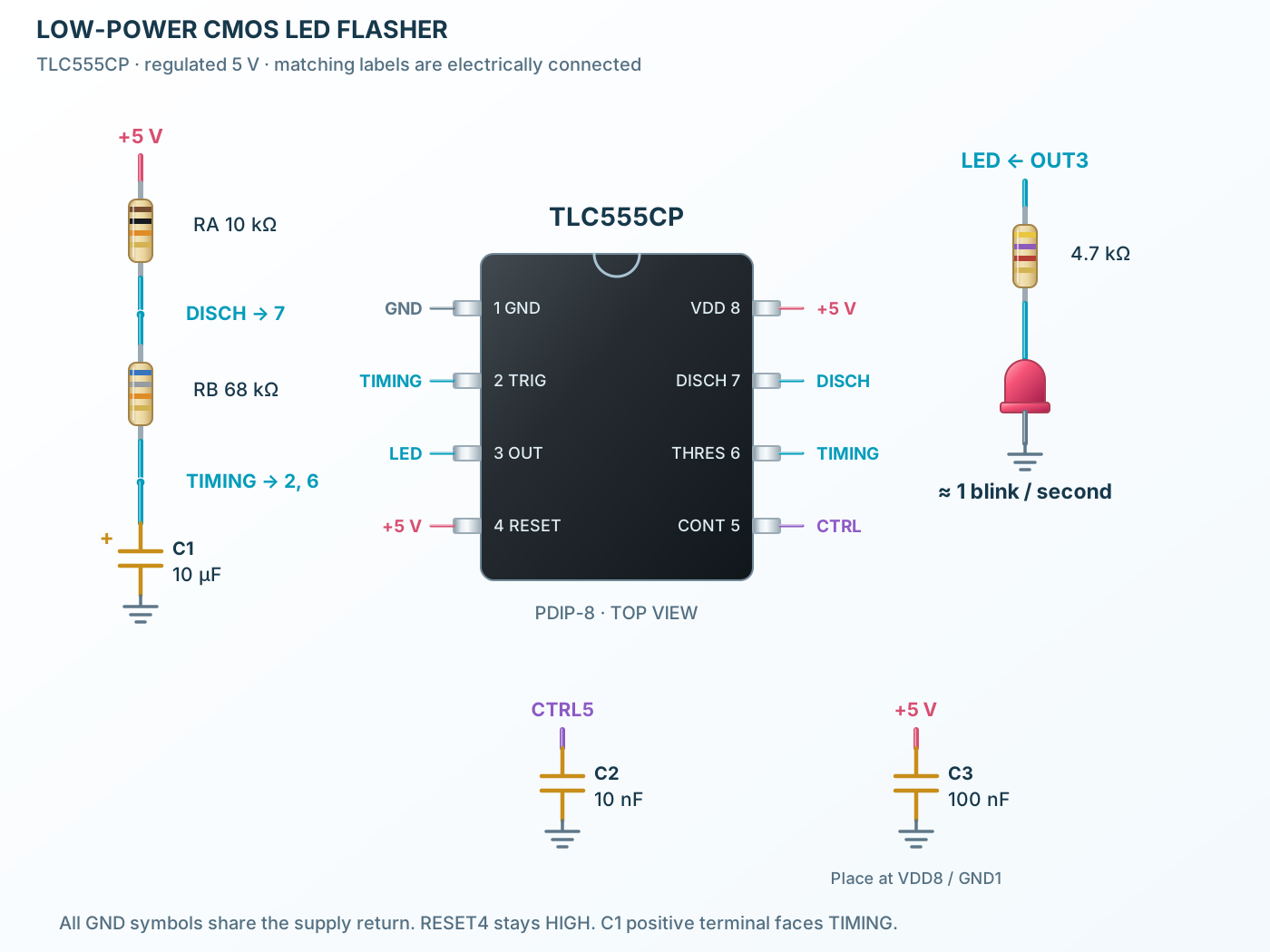
Connect it, step by step
Follow the component values and pin connections
Timing network
Connect RA to VDD and RB between DISCH and the joined timing inputs.
Controls
Tie RESET HIGH and bypass CONT to ground.
Indicator
Drive the LED through 4.7 kΩ; use an external stage for heavier loads.
Inside TLC555
CMOS comparators, latch and output inside one IC.
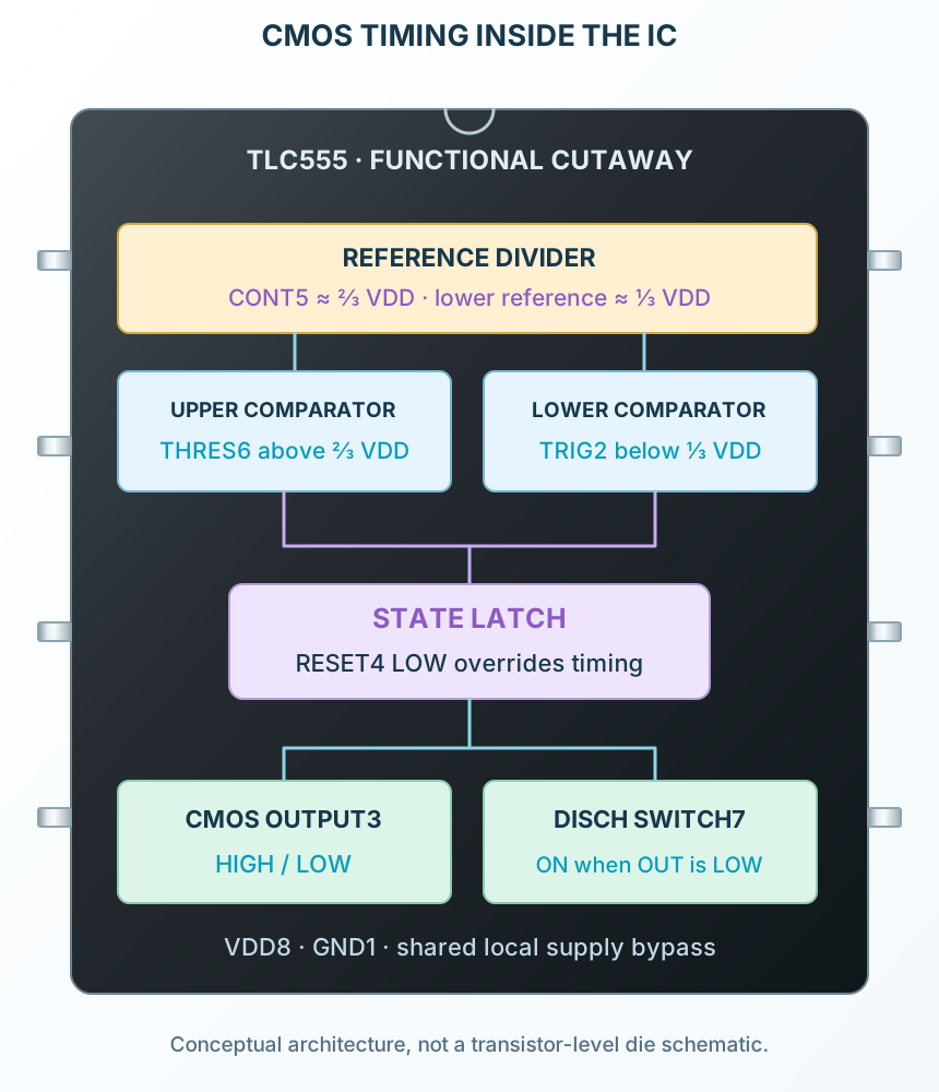
Explore the circuit
Select a stage to see its role and connections
Compare
Two thresholds establish the timing window.
Remember
The latch retains its state between crossings.
Switch
CMOS output and discharge paths change together.
Selected packagePDIP-8TLC555CP
Physical connections8 pinsPackage-specific numbering
Reference collection7 tables36 parameters & pin functions
Pin reference
Signal names, electrical functions and connection guidance
Physical pin numbers8 pins
Scroll within the table to see all columns and rows.
| Pin | Signal | Type | Function & connection |
|---|---|---|---|
| GND | Supply return | Common reference for the timer.Connection guidanceConnect to circuit ground. | |
| TRIG | Trigger input | Below approximately one-third VDD sets the latch when RESET is inactive.Connection guidanceJoin THRES6 at the timing capacitor node. A sustained LOW trigger can hold the output HIGH. | |
| OUT | CMOS output | Push-pull timing output.Connection guidanceDrive an LED through 4.7 kΩ to ground. Output voltage depends on load. Source capability is lower than sink capability. | |
| RESET | Active-LOW reset | Overrides the comparators, forcing OUT LOW and DISCH conducting.Connection guidanceTie to VDD for continuous oscillation. Never leave RESET floating. | |
| CONT | Comparator reference | Approximately two-thirds VDD with no external drive.Connection guidanceBypass to ground with 10 nF. Changing CONT changes timing thresholds and equations. | |
| THRES | Threshold input | Above CONT resets the latch when TRIG is above its lower threshold.Connection guidanceJoin TRIG2 at the timing capacitor node. | |
| DISCH | Discharge switch | Provides a low-impedance path to ground while OUT is LOW.Connection guidanceConnect to the RA/RB junction. Not a second push-pull output. | |
| VDD | Positive supply | Power for the CMOS timer.Connection guidanceApply +5 V; bypass to GND1 locally with 100 nF. Selected TLC555C grade: recommended 2–15 V, 0–70°C. |
No pins match these filters. Try another signal name or reset the filters.
Recommended operation
TLC555CP / TLC555CDR
Manufacturer-referenced values5 parameters
Scroll within the table to see all columns and rows.
| Parameter | Value | Conditions / notes |
|---|---|---|
| Supply | 2–15 V | C grade; example uses 5 V |
| Ambient | 0 to +70°C | C grade in either selected package |
| Industrial grade comparison | 3–15 V; −40 to +85°C | TLC555I, not the selected parts |
| Nominal timing window | 1/3 to 2/3 VDD | CONT unmodulated |
| Typical output capabilities | 100 mA sink; 10 mA source | Feature values, not guaranteed rail-level drive |
No specifications match. Try a parameter name or a unit.
Observe the electrical test conditions and thermal limits; output capability is asymmetric.
Five-volt electrical limits
25°C unless stated
Manufacturer-referenced values8 parameters
Scroll within the table to see all columns and rows.
| Parameter | Value | Conditions / notes |
|---|---|---|
| Supply current | 180 µA typical; 350 µA max | 5 V; expected timing configurations |
| Supply current over C-grade temperature | 500 µA max | 5 V; 0–70°C |
| Trigger threshold | 1.36–1.96 V; 1.66 V typical | 5 V, 25°C |
| Upper threshold | 2.8–3.8 V; 3.3 V typical | 5 V, 25°C |
| HIGH output | 4.8 V typical; 4.1 V minimum | Sourcing 1 mA |
| LOW output | 0.21 V typical; 0.4 V maximum | Sinking 8 mA |
| Timing-input current | 10 pA typical | 25°C; TRIG and THRES |
| Timing-input capacitance | 2.1 pF typical | Each timing input |
No specifications match. Try a parameter name or a unit.
Typical values describe characterization, not guaranteed performance for every device.
Nominal timing equations
Standard two-resistor astable
Manufacturer-referenced values5 parameters
Scroll within the table to see all columns and rows.
| Parameter | Value | Conditions / notes |
|---|---|---|
| HIGH time | ln(2) × (RA + RB) × C | Charging interval |
| LOW time | ln(2) × RB × C | Discharge interval |
| Frequency | 1 / [ln(2) × (RA + 2RB) × C] | Ω, F, seconds |
| HIGH duty cycle | (RA + RB) / (RA + 2RB) | Ordinary astable duty exceeds 50% |
| Monostable duration | Approximately 1.1 × R × C | Clean trigger must release before the interval finishes |
No specifications match. Try a parameter name or a unit.
Initial power-up timing differs from subsequent cycles. Comparator limits, leakage and component tolerance change real timing.
Low-current LED flasher
5 V · nominal 0.988 Hz
Manufacturer-referenced values7 parameters
Scroll within the table to see all columns and rows.
| Parameter | Value | Conditions / notes |
|---|---|---|
| RA / RB | 10 kΩ / 68 kΩ | RA from VDD8 to DISCH7; RB from DISCH7 to TRIG2/THRES6 |
| Timing capacitor | 10 µF | Positive at timing node, negative at ground |
| HIGH / LOW interval | 0.541 / 0.471 s | Ideal steady-state values |
| HIGH duty | 53.42% | LED anode driven through 4.7 kΩ from OUT3 |
| LED current estimate | Approximately 0.64 mA | (5−2)/4700; actual output and LED drops vary |
| RESET / CONT | 4 to VDD; 5 through 10 nF to GND | No floating controls |
| Local bypass | 100 nF | VDD8 directly to GND1 |
No specifications match. Try a parameter name or a unit.
All ground symbols are the same return. Use a driver for larger loads.
Input priority
RESET first, then trigger
Manufacturer-referenced values4 parameters
Scroll within the table to see all columns and rows.
| Parameter | Value | Conditions / notes |
|---|---|---|
| RESET LOW | OUT LOW; DISCH ON | Overrides the timing inputs |
| TRIG below lower threshold | OUT HIGH; DISCH OFF | RESET inactive |
| THRES above upper threshold | OUT LOW; DISCH ON | TRIG above lower threshold |
| Both between thresholds | Latch retains state | No new threshold crossing |
No specifications match. Try a parameter name or a unit.
The ordinary timing equations assume CONT is bypassed and RESET is HIGH.
Package and absolute limits
TLC555CP · PDIP-8
Manufacturer-referenced values7 parameters
Scroll within the table to see all columns and rows.
| Parameter | Value | Conditions / notes |
|---|---|---|
| Pitch | 2.54 mm | Through-hole |
| Absolute supply | −0.3 to +18 V | Stress rating, not the 15 V operating limit |
| Absolute input | −0.3 V to VDD | Any input |
| Absolute output/discharge sink | 150 mA | Stress limit, not recommended continuous loading |
| Absolute output source | 15 mA | Stress limit |
| Storage | −65 to +150°C | Unpowered |
| Junction-to-ambient reference | 93.1°C/W PDIP; 138.9°C/W SOIC | TI thermal test conditions; board-dependent |
No specifications match. Try a parameter name or a unit.
Do not design continuous operation at an absolute maximum.
No matching rowsTry a pin name, parameter, unit or test condition, or reset the filters.
Low-power oscillators
Generate moderate-frequency clocks with a suitable RC network.
Manufacturer application guideOne-shot timing
Create a single pulse from a defined trigger.
Manufacturer application guidePulse-width control
Use the control input to alter timing, respecting the manufacturer application circuits.
Manufacturer application guideTake it into ProTech
Find TLC555 in the Components Library to place its schematic symbol and connect its pins.
Reference page · circuit simulation model not yet availableOpen ProTech