UC3842ACurrent-mode PWM controller
Start a pulse. Measure current. End it at the threshold.
UC3842A is a current-mode PWM controller with an oscillator, voltage-error amplifier, current comparator, latch and gate driver. It begins a switching pulse with the oscillator and ends it when the sensed current reaches the threshold requested by the feedback loop. This variant uses a nominal 16 V startup threshold and a 10 V turn-off threshold. It can operate near full duty cycle; it must not be confused with the lower-startup UC3843A or the half-duty UC3844A and UC3845A variants. The example uses an 18 V bench supply, an RC oscillator and an adjustable low-voltage signal at ISENSE. It demonstrates pulse truncation on a scope without a power MOSFET, transformer or mains connection. The selected eight-pin packages keep the same electrical pin numbers.
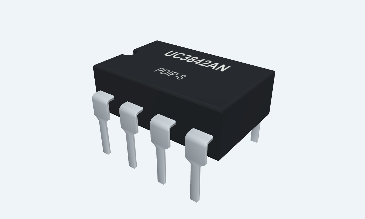
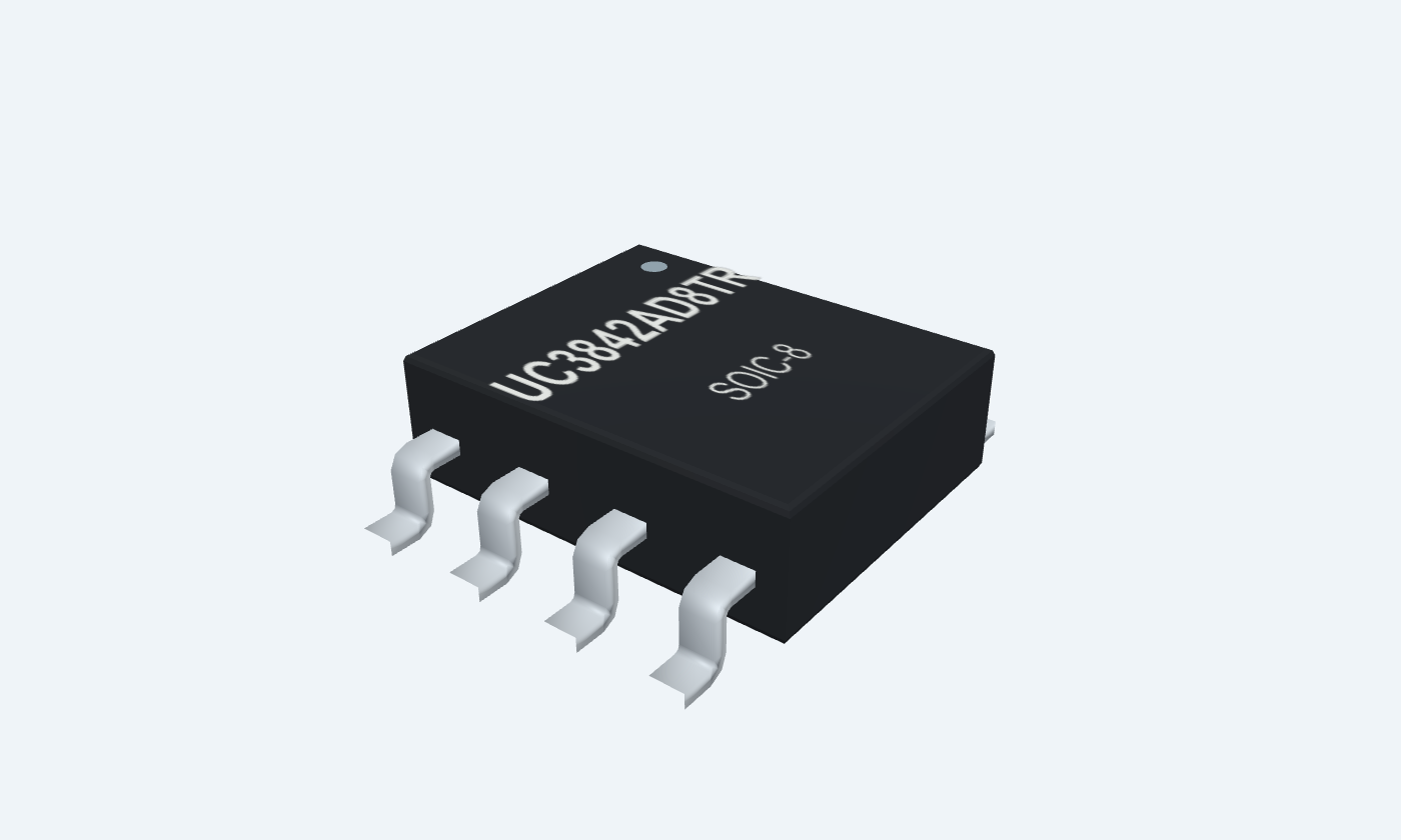

8Physical pins
UC3842ANPDIP-8
Manufacturer-referencedTexas Instruments
Pin diagram
Select a pin to explore its connection
Highlight
UC3842ANPDIP-8Top view
UC3842ASOIC-8Top view
Click a lead or use the arrow keys. Top view
PIN 1 · Feedback compensation
Error-amplifier outputCOMP
Function
Controls the current comparator threshold and accepts the loop-compensation network.
How to connect
Leave externally open in the fixed-demand bench circuit.
Electrical note
Do not force the node against its amplifier drive.
PIN 2 · Feedback and current sense
Voltage feedbackFB
Function
Inverting error-amplifier input, compared with an internal nominal 2.5 V reference.
How to connect
Ground in this open-loop scope demonstration to request the maximum current threshold.
Electrical note
A real regulated converter needs feedback and compensation; this example has no power stage.
PIN 3 · Feedback and current sense
Current-sense inputISENSE
Function
Ends an output pulse when the sense voltage exceeds the COMP-derived threshold; the maximum threshold is approximately 1 V.
How to connect
Feed a 0–1.25 V control through 1 kΩ, with 1 nF to GND at the input.
Electrical note
DC above the threshold can leave very short pulses because turn-off has propagation delay.
PIN 4 · RC oscillator
Oscillator timing nodeRT/CT
Function
Connects both the charging resistor and timing capacitor.
How to connect
Use RT = 10 kΩ from VREF8 to this pin and CT = 3.3 nF from this pin to GND.
Electrical note
RT returns to VREF, not to ground.
PIN 5 · Ground
Common returnGND
Function
Control and driver return in the selected eight-pin packages.
How to connect
Join timing, bypass, control and scope grounds locally.
PIN 6 · Gate driver
Totem-pole gate driverOUTPUT
Function
Pulsed output intended to drive an external power switch through a suitable gate resistor.
How to connect
Connect a high-impedance scope and a 10 kΩ load to GND in this demonstration.
Electrical note
The 1 A headline is peak driver capability, not a continuous load supply.
PIN 7 · Supply
Controller and driver supplyVCC
Function
Undervoltage lockout keeps OUTPUT low until startup voltage is reached.
How to connect
Use regulated +18 V with 10 µF and 100 nF local bypass.
Electrical note
UC3842A starts around 16 V; a 12 V supply may never start it.
PIN 8 · Bias reference
5 V referenceVREF
Function
Bias and oscillator supply available after startup.
How to connect
Bypass with 1 µF; feed RT and the low-current sense-control network.
Electrical note
Keep normal external reference load at or below 10 mA.
Key specifications
COMP sets the sense threshold below an internal clamp. The output latch prevents a second full pulse until the next clock cycle.
Typical startup16 V · UC3842A
Maximum sense threshold1 V typical
Oscillator capability500 kHz maximum
Selected ambient0–70 °C
Package details
UC3842AN · PDIP-8
| Property | Details |
|---|---|
| Manufacturer | Texas Instruments |
| Part number | UC3842AN |
| Package | PDIP-8 |
| Connections | 8 pins |
| Mounting | Through-hole |
| Lead pitch | 2.54 mm |
| Package code | PDIP-8 |
| Thermal reference | See operating and package limits |
Startup and bias
UC3842A variant only
Manufacturer specifications 6 parameters
Scroll sideways to see all columns.
| Parameter | Value | Conditions / notes |
|---|---|---|
| Startup threshold | 14.5–17.5 V; 16 V typical | VCC rising |
| Turn-off threshold | 8.5–11.5 V; 10 V typical | VCC falling after turn-on |
| Example supply | 18 V regulated | Allows margin above the maximum startup threshold |
| Startup current | 0.3 mA typical; 0.5 mA maximum | Specified test conditions |
| Operating supply current | 11 mA typical; 17 mA maximum | FB and ISENSE grounded; unloaded test conditions |
| Ambient temperature | 0 to +70°C | Selected UC3842A grade |
No specifications match. Try a parameter name or a unit.
The shared family operating table does not override the UC3842A startup threshold.
Reference and feedback
UC384xA specifications
Manufacturer specifications 7 parameters
Scroll sideways to see all columns.
| Parameter | Value | Conditions / notes |
|---|---|---|
| Initial VREF | 4.9–5.1 V; 5 V typical | TJ = 25°C, IO = 1 mA |
| Total VREF variation | 4.82–5.18 V | Specified line, load and temperature |
| Normal VREF load | 10 mA maximum | Reference supplies timing and control networks |
| VREF bypass | 1 µF | Close to VREF8 and GND5 |
| FB regulation reference | 2.42–2.58 V; 2.5 V typical | VCOMP = 2.5 V |
| Amplifier unity bandwidth | 1 MHz typical; 0.7 MHz minimum | Manufacturer test conditions |
| Amplifier output | COMP1 | Compensation and current-demand control |
No specifications match. Try a parameter name or a unit.
VREF is not a motor or general power-supply output.
Timing and pulse limits
Eight-pin RT/CT4
Manufacturer specifications 7 parameters
Scroll sideways to see all columns.
| Parameter | Value | Conditions / notes |
|---|---|---|
| RT connection | VREF8 to RT/CT4 | Recommended resistor range 5–100 kΩ |
| CT connection | RT/CT4 to GND5 | Recommended capacitance 470 pF–4.7 nF |
| Example network | 10 kΩ and 3.3 nF | Matches the electrical-characteristic timing setup |
| Initial frequency | 47–57 kHz; 52 kHz typical | TJ = 25°C and stated datasheet conditions |
| Typical period | About 19.2 µs | 1 / 52 kHz |
| Maximum duty capability | 92% minimum; 96% typical | UC3842A test conditions |
| Other family members | UC3844A / UC3845A limit duty to about half | Do not mix their timing behavior with this page |
No specifications match. Try a parameter name or a unit.
Frequency and maximum duty are affected by discharge current and the RC network.
Current comparator
Voltage determines external peak current
Manufacturer specifications 7 parameters
Scroll sideways to see all columns.
| Parameter | Value | Conditions / notes |
|---|---|---|
| Maximum sense input | 0.9–1.1 V; 1 V typical | VCOMP = 5 V; specified test |
| Sense control gain | 2.85–3.15 V/V; 3 typical | Specified current-sense transfer |
| Comparator delay | 150 ns typical; 300 ns maximum | ISENSE transition from 0 to 2 V |
| Shunt relationship | IPK ≈ VTRIP / RSENSE | Ignores propagation overshoot and filtering |
| Illustrative 0.5 Ω shunt | 1 V / 0.5 Ω = 2 A | Calculation only; no shunt or power stage in the bench demo |
| DC sense above threshold | Pulses are cut short | Propagation delay can leave narrow pulses |
| Duty above 50% | Slope compensation may be needed | Current-mode subharmonic behavior must be checked |
No specifications match. Try a parameter name or a unit.
Actual power-stage peak current also depends on delay, noise filtering, tolerances and inductor current slope.
18 V scope circuit
Observe current-comparator action
Manufacturer specifications 8 parameters
Scroll sideways to see all columns.
| Parameter | Value | Conditions / notes |
|---|---|---|
| VCC7 / GND5 | 18 V / common return | 10 µF and 100 nF local supply bypass |
| VREF8 | 1 µF bypass | Feeds RT and the sense-control divider |
| RT / CT | 10 kΩ from REF to pin 4; 3.3 nF from pin 4 to GND | Keep timing traces short |
| FB2 / COMP1 | GND / no external connection | Maximum current demand in this demonstration |
| Sense control | 30 kΩ in series with a 10 kΩ pot across REF/GND | Pot wiper gives approximately 0–1.25 V |
| ISENSE3 filter | Wiper through 1 kΩ; 1 nF from pin 3 to GND | Reduces wiper noise; not a power-stage filter design |
| OUTPUT6 | High-impedance scope plus 10 kΩ to GND | No transformer or switching MOSFET |
| Control action | Raise sense voltage from zero | Observe pulse truncation near the comparator threshold |
No specifications match. Try a parameter name or a unit.
All grounds share one return. The output can reach near VCC; use a properly rated probe.
Output and layout
Totem-pole gate drive
Manufacturer specifications 6 parameters
Scroll sideways to see all columns.
| Parameter | Value | Conditions / notes |
|---|---|---|
| Peak output capability | Up to ±1 A | Peak gate drive; observe thermal and pulse limits |
| LOW at 20 mA sink | 0.1 V typical; 0.4 V maximum | Specified VCC = 15 V test |
| HIGH at 20 mA source | 13.5 V typical; 13 V minimum | Specified VCC = 15 V test |
| External MOSFET connection | Use a suitable gate resistor | Limits peak gate charging current |
| Supply bypass sizing | VCC capacitance at least 10× VREF bypass | Also account for power-switch gate capacitance |
| Ground arrangement | Short local timing and sense returns | Keep gate-current loops away from analog inputs |
No specifications match. Try a parameter name or a unit.
The eight-pin version shares power and signal ground internally; larger packages have additional pins.
Packages and absolute limits
UC3842AN · PDIP-8
Manufacturer specifications 7 parameters
Scroll sideways to see all columns.
| Parameter | Value | Conditions / notes |
|---|---|---|
| PDIP reference | UC3842AN · 8 pins | TI P; current appendix marks NRND |
| SMD reference | UC3842AD8TR · 8 pins | TI D8; active orderable in reviewed appendix |
| Different SMD ordering | UC3842AD · 14 pins | Different pin map; not represented by this eight-pin preview |
| VCC absolute maximum | 30 V from a low-impedance source | Stress limit; not a recommended operating target |
| Analog-input absolute range | −0.3 to +6.3 V | Recommended analog limits are tighter |
| Storage temperature | −65 to +150°C | Unpowered |
| Output capacitive energy | 5 µJ absolute maximum | Check driver dissipation and repetition |
No specifications match. Try a parameter name or a unit.
Use exact suffixes and manufacturer drawings when selecting a package.
Connections by function
Select a pin for its function, connection guidance and electrical notes.
Feedback compensation1 pin
Feedback and current sense2 pins
RC oscillator1 pin
Ground1 pin
Gate driver1 pin
Supply1 pin
Bias reference1 pin
Feedback compensation1 pin
Feedback and current sense2 pins
RC oscillator1 pin
Ground1 pin
Gate driver1 pin
Supply1 pin
Bias reference1 pin
UC3842A at a glance
Follow the labeled connections and functional stages
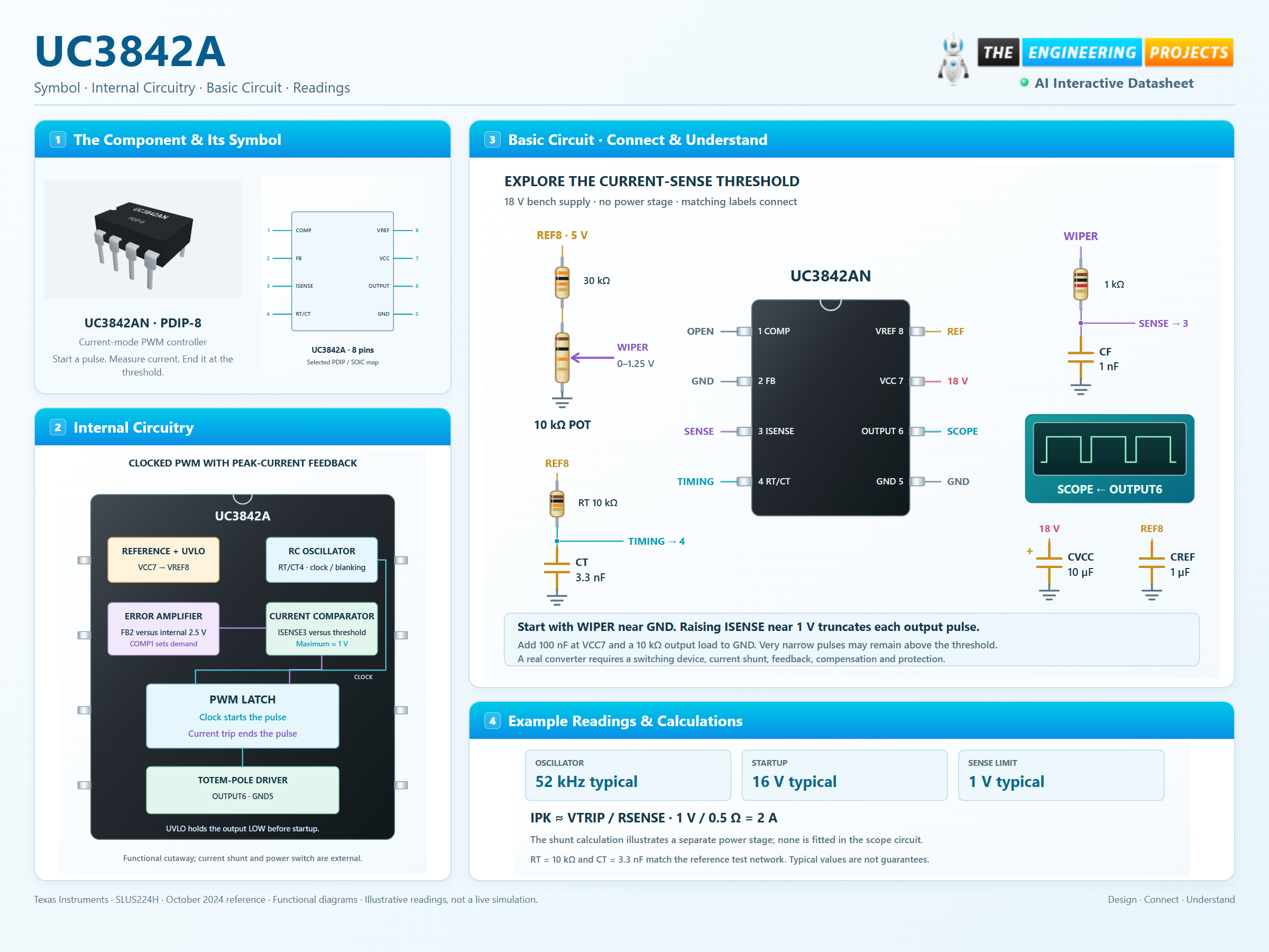
How it works
3 stages · Explore one step at a time
Cross the startup threshold
VCC must first reach the start threshold. After startup, hysteresis permits operation at a lower voltage.
Set the peak-current demand
The error amplifier compares FB with 2.5 V. COMP programs the current-comparator trip point, up to the internal limit.
Terminate the pulse
A sufficiently high ISENSE signal resets the PWM latch. Oscillator blanking also limits maximum duty.
Step 1 of 3
UC3842A in a circuit
An RC oscillator, a low-voltage control and a scope.
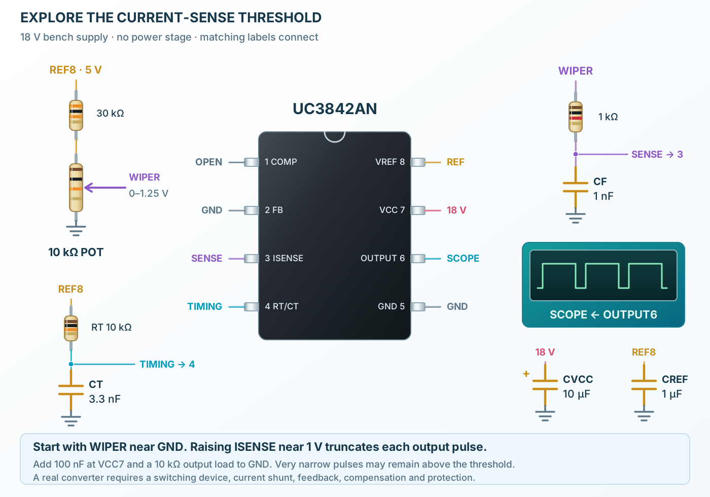
Connect it, step by step
Follow the component values and pin connections
Provide startup headroom
An 18 V supply exceeds the specified maximum start threshold. A 12 V supply is not sufficient for guaranteed cold startup.
Connect the oscillator
RT connects to VREF and CT connects to ground, meeting at pin 4.
Raise the sense input
Increase the pot wiper from zero toward 1.25 V and observe shorter pulses. Very narrow pulses may remain above the threshold.
Inside UC3842A
Reference, current comparator and a clocked PWM latch.
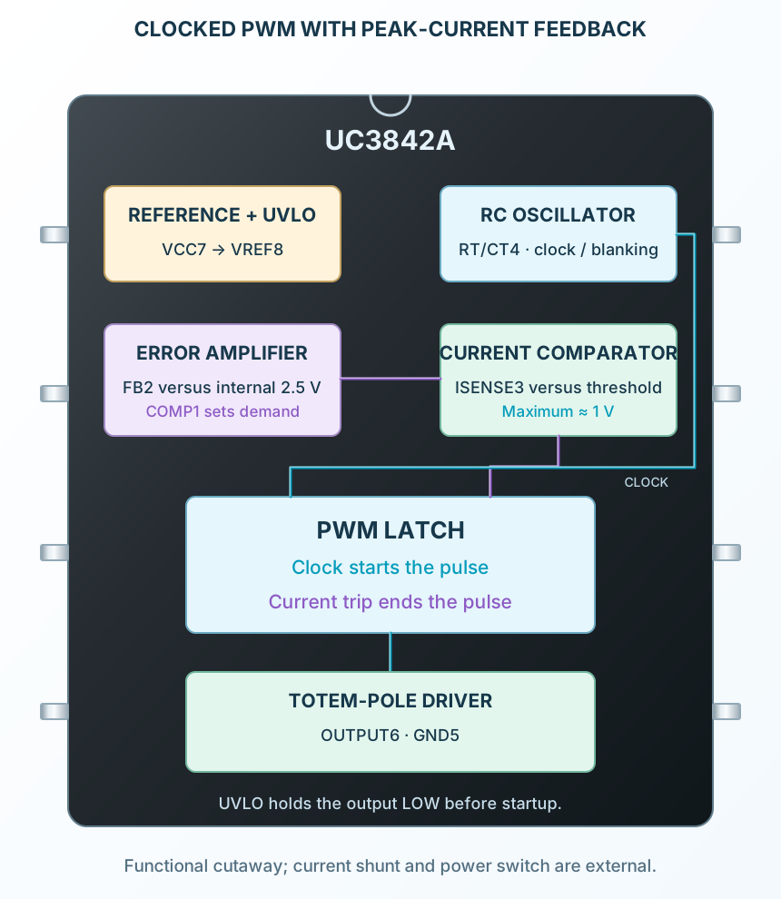
Explore the circuit
Select a stage to see its role and connections
Establish the references
UVLO controls startup. VREF supplies timing and the feedback reference.
Compare sensed current
COMP sets a threshold for ISENSE, bounded by the internal clamp.
Reset the PWM latch
A current trip ends the pulse; the next oscillator cycle allows a new one.
Selected packagePDIP-8UC3842AN
Physical connections8 pinsPackage-specific numbering
Reference collection8 tables48 parameters & pin functions
Pin reference
Signal names, electrical functions and connection guidance
Physical pin numbers8 pins
Scroll within the table to see all columns and rows.
| Pin | Signal | Type | Function & connection |
|---|---|---|---|
| COMP | Error-amplifier output | Controls the current comparator threshold and accepts the loop-compensation network.Connection guidanceLeave externally open in the fixed-demand bench circuit. Do not force the node against its amplifier drive. | |
| FB | Voltage feedback | Inverting error-amplifier input, compared with an internal nominal 2.5 V reference.Connection guidanceGround in this open-loop scope demonstration to request the maximum current threshold. A real regulated converter needs feedback and compensation; this example has no power stage. | |
| ISENSE | Current-sense input | Ends an output pulse when the sense voltage exceeds the COMP-derived threshold; the maximum threshold is approximately 1 V.Connection guidanceFeed a 0–1.25 V control through 1 kΩ, with 1 nF to GND at the input. DC above the threshold can leave very short pulses because turn-off has propagation delay. | |
| RT/CT | Oscillator timing node | Connects both the charging resistor and timing capacitor.Connection guidanceUse RT = 10 kΩ from VREF8 to this pin and CT = 3.3 nF from this pin to GND. RT returns to VREF, not to ground. | |
| GND | Common return | Control and driver return in the selected eight-pin packages.Connection guidanceJoin timing, bypass, control and scope grounds locally. | |
| OUTPUT | Totem-pole gate driver | Pulsed output intended to drive an external power switch through a suitable gate resistor.Connection guidanceConnect a high-impedance scope and a 10 kΩ load to GND in this demonstration. The 1 A headline is peak driver capability, not a continuous load supply. | |
| VCC | Controller and driver supply | Undervoltage lockout keeps OUTPUT low until startup voltage is reached.Connection guidanceUse regulated +18 V with 10 µF and 100 nF local bypass. UC3842A starts around 16 V; a 12 V supply may never start it. | |
| VREF | 5 V reference | Bias and oscillator supply available after startup.Connection guidanceBypass with 1 µF; feed RT and the low-current sense-control network. Keep normal external reference load at or below 10 mA. |
No pins match these filters. Try another signal name or reset the filters.
Startup and bias
UC3842A variant only
Manufacturer-referenced values6 parameters
Scroll within the table to see all columns and rows.
| Parameter | Value | Conditions / notes |
|---|---|---|
| Startup threshold | 14.5–17.5 V; 16 V typical | VCC rising |
| Turn-off threshold | 8.5–11.5 V; 10 V typical | VCC falling after turn-on |
| Example supply | 18 V regulated | Allows margin above the maximum startup threshold |
| Startup current | 0.3 mA typical; 0.5 mA maximum | Specified test conditions |
| Operating supply current | 11 mA typical; 17 mA maximum | FB and ISENSE grounded; unloaded test conditions |
| Ambient temperature | 0 to +70°C | Selected UC3842A grade |
No specifications match. Try a parameter name or a unit.
The shared family operating table does not override the UC3842A startup threshold.
Reference and feedback
UC384xA specifications
Manufacturer-referenced values7 parameters
Scroll within the table to see all columns and rows.
| Parameter | Value | Conditions / notes |
|---|---|---|
| Initial VREF | 4.9–5.1 V; 5 V typical | TJ = 25°C, IO = 1 mA |
| Total VREF variation | 4.82–5.18 V | Specified line, load and temperature |
| Normal VREF load | 10 mA maximum | Reference supplies timing and control networks |
| VREF bypass | 1 µF | Close to VREF8 and GND5 |
| FB regulation reference | 2.42–2.58 V; 2.5 V typical | VCOMP = 2.5 V |
| Amplifier unity bandwidth | 1 MHz typical; 0.7 MHz minimum | Manufacturer test conditions |
| Amplifier output | COMP1 | Compensation and current-demand control |
No specifications match. Try a parameter name or a unit.
VREF is not a motor or general power-supply output.
Timing and pulse limits
Eight-pin RT/CT4
Manufacturer-referenced values7 parameters
Scroll within the table to see all columns and rows.
| Parameter | Value | Conditions / notes |
|---|---|---|
| RT connection | VREF8 to RT/CT4 | Recommended resistor range 5–100 kΩ |
| CT connection | RT/CT4 to GND5 | Recommended capacitance 470 pF–4.7 nF |
| Example network | 10 kΩ and 3.3 nF | Matches the electrical-characteristic timing setup |
| Initial frequency | 47–57 kHz; 52 kHz typical | TJ = 25°C and stated datasheet conditions |
| Typical period | About 19.2 µs | 1 / 52 kHz |
| Maximum duty capability | 92% minimum; 96% typical | UC3842A test conditions |
| Other family members | UC3844A / UC3845A limit duty to about half | Do not mix their timing behavior with this page |
No specifications match. Try a parameter name or a unit.
Frequency and maximum duty are affected by discharge current and the RC network.
Current comparator
Voltage determines external peak current
Manufacturer-referenced values7 parameters
Scroll within the table to see all columns and rows.
| Parameter | Value | Conditions / notes |
|---|---|---|
| Maximum sense input | 0.9–1.1 V; 1 V typical | VCOMP = 5 V; specified test |
| Sense control gain | 2.85–3.15 V/V; 3 typical | Specified current-sense transfer |
| Comparator delay | 150 ns typical; 300 ns maximum | ISENSE transition from 0 to 2 V |
| Shunt relationship | IPK ≈ VTRIP / RSENSE | Ignores propagation overshoot and filtering |
| Illustrative 0.5 Ω shunt | 1 V / 0.5 Ω = 2 A | Calculation only; no shunt or power stage in the bench demo |
| DC sense above threshold | Pulses are cut short | Propagation delay can leave narrow pulses |
| Duty above 50% | Slope compensation may be needed | Current-mode subharmonic behavior must be checked |
No specifications match. Try a parameter name or a unit.
Actual power-stage peak current also depends on delay, noise filtering, tolerances and inductor current slope.
18 V scope circuit
Observe current-comparator action
Manufacturer-referenced values8 parameters
Scroll within the table to see all columns and rows.
| Parameter | Value | Conditions / notes |
|---|---|---|
| VCC7 / GND5 | 18 V / common return | 10 µF and 100 nF local supply bypass |
| VREF8 | 1 µF bypass | Feeds RT and the sense-control divider |
| RT / CT | 10 kΩ from REF to pin 4; 3.3 nF from pin 4 to GND | Keep timing traces short |
| FB2 / COMP1 | GND / no external connection | Maximum current demand in this demonstration |
| Sense control | 30 kΩ in series with a 10 kΩ pot across REF/GND | Pot wiper gives approximately 0–1.25 V |
| ISENSE3 filter | Wiper through 1 kΩ; 1 nF from pin 3 to GND | Reduces wiper noise; not a power-stage filter design |
| OUTPUT6 | High-impedance scope plus 10 kΩ to GND | No transformer or switching MOSFET |
| Control action | Raise sense voltage from zero | Observe pulse truncation near the comparator threshold |
No specifications match. Try a parameter name or a unit.
All grounds share one return. The output can reach near VCC; use a properly rated probe.
Output and layout
Totem-pole gate drive
Manufacturer-referenced values6 parameters
Scroll within the table to see all columns and rows.
| Parameter | Value | Conditions / notes |
|---|---|---|
| Peak output capability | Up to ±1 A | Peak gate drive; observe thermal and pulse limits |
| LOW at 20 mA sink | 0.1 V typical; 0.4 V maximum | Specified VCC = 15 V test |
| HIGH at 20 mA source | 13.5 V typical; 13 V minimum | Specified VCC = 15 V test |
| External MOSFET connection | Use a suitable gate resistor | Limits peak gate charging current |
| Supply bypass sizing | VCC capacitance at least 10× VREF bypass | Also account for power-switch gate capacitance |
| Ground arrangement | Short local timing and sense returns | Keep gate-current loops away from analog inputs |
No specifications match. Try a parameter name or a unit.
The eight-pin version shares power and signal ground internally; larger packages have additional pins.
Packages and absolute limits
UC3842AN · PDIP-8
Manufacturer-referenced values7 parameters
Scroll within the table to see all columns and rows.
| Parameter | Value | Conditions / notes |
|---|---|---|
| PDIP reference | UC3842AN · 8 pins | TI P; current appendix marks NRND |
| SMD reference | UC3842AD8TR · 8 pins | TI D8; active orderable in reviewed appendix |
| Different SMD ordering | UC3842AD · 14 pins | Different pin map; not represented by this eight-pin preview |
| VCC absolute maximum | 30 V from a low-impedance source | Stress limit; not a recommended operating target |
| Analog-input absolute range | −0.3 to +6.3 V | Recommended analog limits are tighter |
| Storage temperature | −65 to +150°C | Unpowered |
| Output capacitive energy | 5 µJ absolute maximum | Check driver dissipation and repetition |
No specifications match. Try a parameter name or a unit.
Use exact suffixes and manufacturer drawings when selecting a package.
No matching rowsTry a pin name, parameter, unit or test condition, or reset the filters.
Current-mode converters
Control a separately designed flyback, forward or other compatible power stage.
Manufacturer application guideCycle-by-cycle limiting
Use an external sense network to limit peak switching current.
Manufacturer application guideController bench testing
Inspect the oscillator and comparator response without connecting a power stage.
Manufacturer application guideTake it into ProTech
Find UC3842A in the Components Library to place its schematic symbol and connect its pins.
Reference page · circuit simulation model not yet availableOpen ProTech