Real View
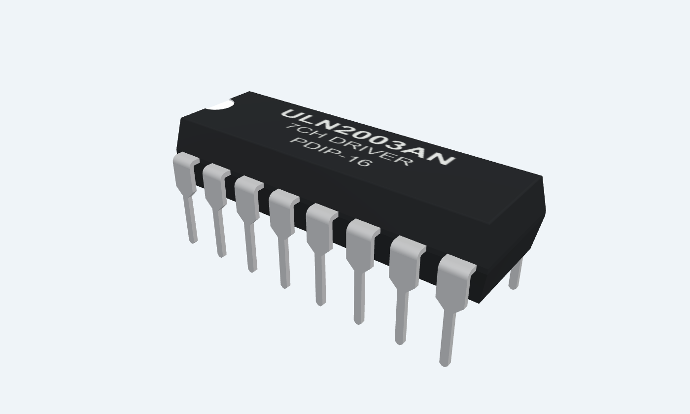
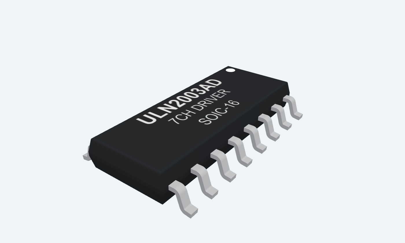
Let low-power logic control relays, lamps and coils.
ULN2003A combines seven NPN Darlington pairs in one 16-pin package. A logic HIGH turns on its matching collector output, allowing the IC to sink current from an external load. Each channel includes a 2.7 kΩ input resistor and a clamp diode. The diode cathodes share COM, which connects to the positive supply when driving relay or motor coils. This reference covers ULN2003AN and ULN2003AD. A 12 V relay example explains the common ground, voltage drop and package power budget.
Select a pin to explore its connection
Click a lead or use the arrow keys. Top view
Drives channel 1 through an internal 2.7 kΩ base resistor.
Connect to a 5 V logic output. Tie unused inputs LOW.
HIGH turns the corresponding low-side output on.
Drives channel 2 through an internal 2.7 kΩ base resistor.
Connect to a 5 V logic output. Tie unused inputs LOW.
HIGH turns the corresponding low-side output on.
Drives channel 3 through an internal 2.7 kΩ base resistor.
Connect to a 5 V logic output. Tie unused inputs LOW.
HIGH turns the corresponding low-side output on.
Drives channel 4 through an internal 2.7 kΩ base resistor.
Connect to a 5 V logic output. Tie unused inputs LOW.
HIGH turns the corresponding low-side output on.
Drives channel 5 through an internal 2.7 kΩ base resistor.
Connect to a 5 V logic output. Tie unused inputs LOW.
HIGH turns the corresponding low-side output on.
Drives channel 6 through an internal 2.7 kΩ base resistor.
Connect to a 5 V logic output. Tie unused inputs LOW.
HIGH turns the corresponding low-side output on.
Drives channel 7 through an internal 2.7 kΩ base resistor.
Connect to a 5 V logic output. Tie unused inputs LOW.
HIGH turns the corresponding low-side output on.
Shared emitter and substrate return for all seven channels.
Connect to load-supply ground and controller ground.
This is the high-current return path; route it appropriately.
Common cathodes of the seven internal flyback diodes.
Connect to the positive relay or motor-coil supply for inductive loads.
COM is not a logic supply pin and is not ground.
Collector output of channel 7.
Connect between the load and the IC; the other load terminal goes to the positive load supply.
Sinks current only. Allow Darlington voltage drop and package heating.
Collector output of channel 6.
Connect between the load and the IC; the other load terminal goes to the positive load supply.
Sinks current only. Allow Darlington voltage drop and package heating.
Collector output of channel 5.
Connect between the load and the IC; the other load terminal goes to the positive load supply.
Sinks current only. Allow Darlington voltage drop and package heating.
Collector output of channel 4.
Connect between the load and the IC; the other load terminal goes to the positive load supply.
Sinks current only. Allow Darlington voltage drop and package heating.
Collector output of channel 3.
Connect between the load and the IC; the other load terminal goes to the positive load supply.
Sinks current only. Allow Darlington voltage drop and package heating.
Collector output of channel 2.
Connect between the load and the IC; the other load terminal goes to the positive load supply.
Sinks current only. Allow Darlington voltage drop and package heating.
Collector output of channel 1.
Connect between the load and the IC; the other load terminal goes to the positive load supply.
Sinks current only. Allow Darlington voltage drop and package heating.
The chip switches the low side of each load. COM serves the clamp diodes; it does not power the input logic.
ULN2003AN · PDIP-16
| Property | Details |
|---|---|
| Manufacturer | Texas Instruments |
| Part number | ULN2003AN |
| Package | PDIP-16 |
| Connections | 16 pins |
| Mounting | Through-hole |
| Lead pitch | 2.54 mm |
| Package code | dip |
| Thermal reference | Board and package dependent; see manufacturer data |
Input and output pairs
Scroll sideways to see all columns.
| Parameter | Value | Conditions / notes |
|---|---|---|
| Channel 1 | 1B pin 1 → 1C pin 16 | HIGH input turns the output sink on |
| Channel 2 | 2B pin 2 → 2C pin 15 | Same behavior |
| Channel 3 | 3B pin 3 → 3C pin 14 | Same behavior |
| Channel 4 | 4B pin 4 → 4C pin 13 | Same behavior |
| Channel 5 | 5B pin 5 → 5C pin 12 | Same behavior |
| Channel 6 | 6B pin 6 → 6C pin 11 | Same behavior |
| Channel 7 | 7B pin 7 → 7C pin 10 | Same behavior |
| Common emitter | E pin 8 | Ground return |
| Diode common | COM pin 9 | Positive inductive-load supply |
No specifications match. Try a parameter name or a unit.
The physical output order is reversed across the package.
ULN2003A · 25°C
Scroll sideways to see all columns.
| Parameter | Value | Conditions / notes |
|---|---|---|
| Input resistor | 2.7 kΩ | Internal series base resistor |
| ON input voltage | 2.4 V maximum | IC = 200 mA; VCE = 2 V |
| ON input voltage | 3.0 V maximum | IC = 300 mA; VCE = 2 V |
| Saturation voltage | 0.9 V typical; 1.1 V maximum | 100 mA collector; 250 µA input |
| Saturation voltage | 1.0 V typical; 1.3 V maximum | 200 mA collector; 350 µA input |
| Saturation voltage | 1.2 V typical; 1.6 V maximum | 350 mA collector; 500 µA input |
| Input current | 0.93 mA typical; 1.35 mA maximum | VI = 3.85 V |
| Clamp diode forward voltage | 1.7 V typical; 2.0 V maximum | IF = 350 mA |
No specifications match. Try a parameter name or a unit.
Use the specified drive current when interpreting the saturation-voltage limits.
Do not add seven maximum channel currents
Scroll sideways to see all columns.
| Parameter | Value | Conditions / notes |
|---|---|---|
| Collector-emitter voltage | 0–50 V | Recommended range; observe transient margin |
| Recommended junction range | −40 to +125°C | Package thermal design matters |
| Peak collector current | 500 mA per channel | Absolute maximum; see duty-cycle curves |
| Total emitter-terminal current | 2.5 A magnitude | Absolute maximum, not a continuous thermal rating |
| Input voltage | 30 V maximum | Absolute maximum; normal control is 5 V logic |
| Clamp current | 500 mA maximum | Absolute maximum per clamp path |
| Maximum junction temperature | 150°C | Absolute maximum |
| Storage | −65 to +150°C | Unpowered |
No specifications match. Try a parameter name or a unit.
A load’s voltage, current and duty cycle must all fit the complete system.
12 V supply · 240 Ω coil
Scroll sideways to see all columns.
| Parameter | Value | Conditions / notes |
|---|---|---|
| Illustrative driver drop | 0.90 V | Fixed teaching estimate; actual value varies |
| Coil voltage when ON | 11.10 V | 12 − 0.90 |
| Coil current when ON | 46.25 mA | 11.10 / 240 |
| Driver dissipation per channel | 41.6 mW | 0.90 × 0.04625 |
| Seven channels ON | 323.75 mA; 291.4 mW | Collector current and output-stage dissipation |
| Relay selection | Check guaranteed pickup voltage | Allow supply, coil and driver tolerances |
No specifications match. Try a parameter name or a unit.
These are DC estimates, not a relay pickup guarantee or transient calculation.
ULN2003AN · PDIP-16
Scroll sideways to see all columns.
| Parameter | Value | Conditions / notes |
|---|---|---|
| Lead pitch | 2.54 mm | Through-hole; top view |
| PDIP-16 RθJA | 66.7°C/W | TI standardized test board |
| SOIC-16 RθJA | 88.6°C/W | TI standardized test board |
| Board dependence | Copper and airflow change temperature | Do not treat RθJA as a universal enclosure constant |
| Unused channels | Inputs LOW; collectors unconnected | Do not leave control inputs floating |
No specifications match. Try a parameter name or a unit.
See the PDF for duty-cycle derating and the exact thermal measurement conditions.
Select a pin for its function, connection guidance and electrical notes.
Follow the labeled connections and functional stages
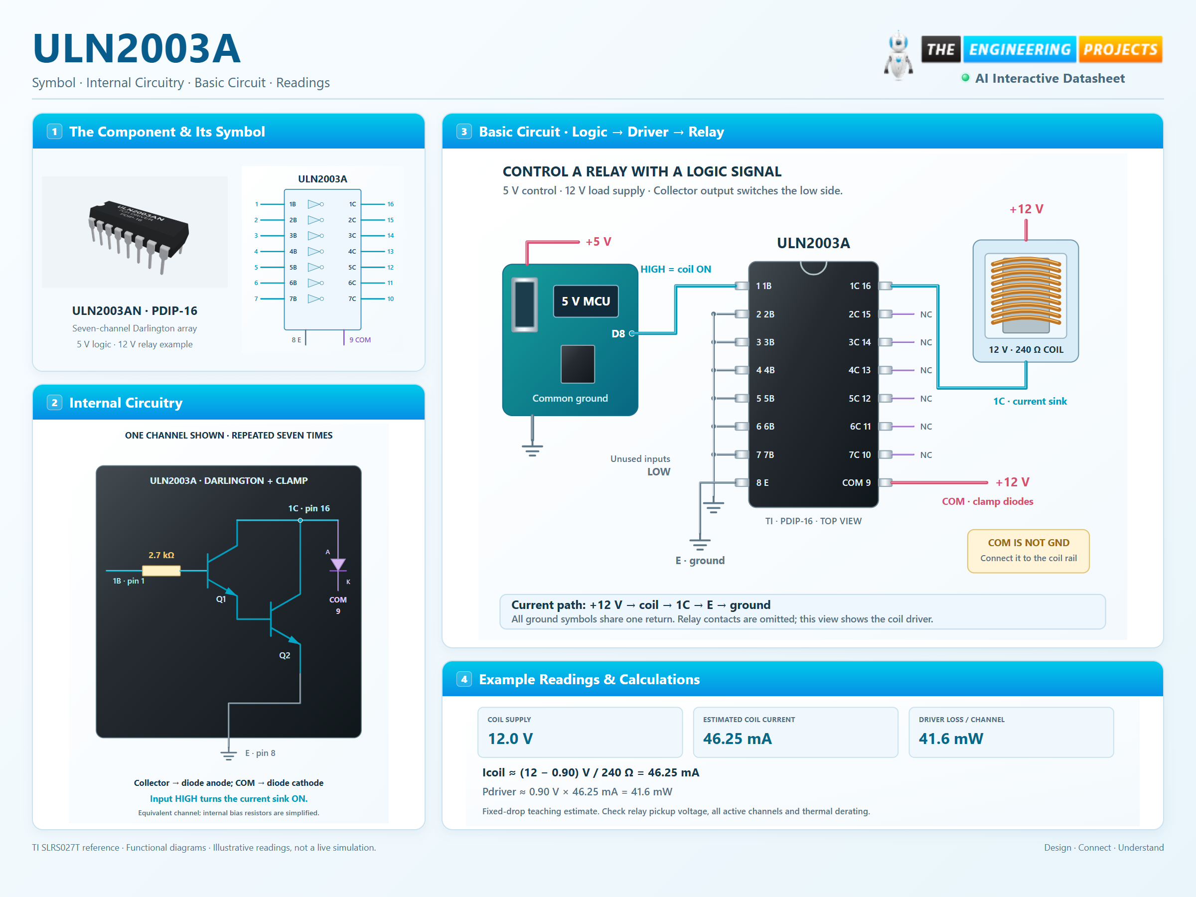
3 stages · Explore one step at a time
A logic HIGH supplies base current through the internal 2.7 kΩ resistor. Two transistors provide current gain in each channel.
The collector sinks current through the load to E. Current flows from the load supply, through the relay coil, through the Darlington pair and back to ground.
When a coil turns off, its current briefly continues through the internal clamp diode to COM. Connect COM to the coil supply and consider how that supply absorbs the energy.
Click an input. Follow its collector current and the combined power budget.
Enable JavaScript to try the drivers.
Illustrative steady-state relay loads. Each coil is 240 Ω on a 12 V supply; the driver drop is fixed at 0.90 V. No relay mechanics, flyback waveform, temperature rise or saturation curve is simulated. COM is connected to the load supply.
A controller signal switches a 12 V coil through channel 1.
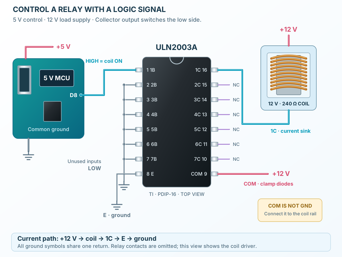
Follow the component values and pin connections
Wire the coil between +12 V and 1C pin 16. Connect E pin 8 to the common ground.
Tie COM pin 9 to the same +12 V rail so the internal diode can carry switch-off current.
A HIGH on 1B pin 1 energizes the coil. LOW releases it. Check pickup voltage with the driver drop included.
Seven input resistors, seven Darlington pairs and seven clamp diodes.
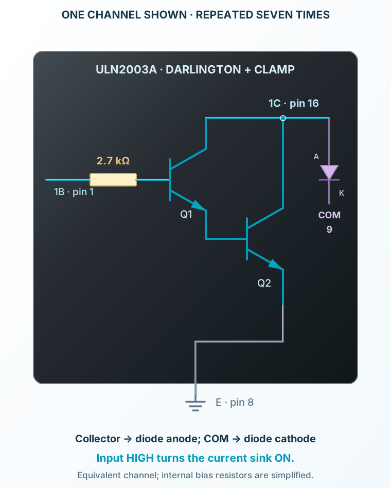
Select a stage to see its role and connections
The first NPN transistor drives the second, increasing current gain.
Both collectors connect to the output. The driver provides a current sink, not a positive voltage source.
The diode anode is at the collector and its cathode is at COM, returning inductive current to the load supply.
Signal names, electrical functions and connection guidance
Scroll within the table to see all columns and rows.
| Pin | Signal | Type | Function & connection |
|---|---|---|---|
| 1B | Darlington input | Drives channel 1 through an internal 2.7 kΩ base resistor.Connection guidanceConnect to a 5 V logic output. Tie unused inputs LOW. HIGH turns the corresponding low-side output on. | |
| 2B | Darlington input | Drives channel 2 through an internal 2.7 kΩ base resistor.Connection guidanceConnect to a 5 V logic output. Tie unused inputs LOW. HIGH turns the corresponding low-side output on. | |
| 3B | Darlington input | Drives channel 3 through an internal 2.7 kΩ base resistor.Connection guidanceConnect to a 5 V logic output. Tie unused inputs LOW. HIGH turns the corresponding low-side output on. | |
| 4B | Darlington input | Drives channel 4 through an internal 2.7 kΩ base resistor.Connection guidanceConnect to a 5 V logic output. Tie unused inputs LOW. HIGH turns the corresponding low-side output on. | |
| 5B | Darlington input | Drives channel 5 through an internal 2.7 kΩ base resistor.Connection guidanceConnect to a 5 V logic output. Tie unused inputs LOW. HIGH turns the corresponding low-side output on. | |
| 6B | Darlington input | Drives channel 6 through an internal 2.7 kΩ base resistor.Connection guidanceConnect to a 5 V logic output. Tie unused inputs LOW. HIGH turns the corresponding low-side output on. | |
| 7B | Darlington input | Drives channel 7 through an internal 2.7 kΩ base resistor.Connection guidanceConnect to a 5 V logic output. Tie unused inputs LOW. HIGH turns the corresponding low-side output on. | |
| E | Common emitter | Shared emitter and substrate return for all seven channels.Connection guidanceConnect to load-supply ground and controller ground. This is the high-current return path; route it appropriately. | |
| COM | Clamp diode common | Common cathodes of the seven internal flyback diodes.Connection guidanceConnect to the positive relay or motor-coil supply for inductive loads. COM is not a logic supply pin and is not ground. | |
| 7C | Open-collector driver | Collector output of channel 7.Connection guidanceConnect between the load and the IC; the other load terminal goes to the positive load supply. Sinks current only. Allow Darlington voltage drop and package heating. | |
| 6C | Open-collector driver | Collector output of channel 6.Connection guidanceConnect between the load and the IC; the other load terminal goes to the positive load supply. Sinks current only. Allow Darlington voltage drop and package heating. | |
| 5C | Open-collector driver | Collector output of channel 5.Connection guidanceConnect between the load and the IC; the other load terminal goes to the positive load supply. Sinks current only. Allow Darlington voltage drop and package heating. | |
| 4C | Open-collector driver | Collector output of channel 4.Connection guidanceConnect between the load and the IC; the other load terminal goes to the positive load supply. Sinks current only. Allow Darlington voltage drop and package heating. | |
| 3C | Open-collector driver | Collector output of channel 3.Connection guidanceConnect between the load and the IC; the other load terminal goes to the positive load supply. Sinks current only. Allow Darlington voltage drop and package heating. | |
| 2C | Open-collector driver | Collector output of channel 2.Connection guidanceConnect between the load and the IC; the other load terminal goes to the positive load supply. Sinks current only. Allow Darlington voltage drop and package heating. | |
| 1C | Open-collector driver | Collector output of channel 1.Connection guidanceConnect between the load and the IC; the other load terminal goes to the positive load supply. Sinks current only. Allow Darlington voltage drop and package heating. |
No pins match these filters. Try another signal name or reset the filters.
Input and output pairs
Scroll within the table to see all columns and rows.
| Parameter | Value | Conditions / notes |
|---|---|---|
| Channel 1 | 1B pin 1 → 1C pin 16 | HIGH input turns the output sink on |
| Channel 2 | 2B pin 2 → 2C pin 15 | Same behavior |
| Channel 3 | 3B pin 3 → 3C pin 14 | Same behavior |
| Channel 4 | 4B pin 4 → 4C pin 13 | Same behavior |
| Channel 5 | 5B pin 5 → 5C pin 12 | Same behavior |
| Channel 6 | 6B pin 6 → 6C pin 11 | Same behavior |
| Channel 7 | 7B pin 7 → 7C pin 10 | Same behavior |
| Common emitter | E pin 8 | Ground return |
| Diode common | COM pin 9 | Positive inductive-load supply |
No specifications match. Try a parameter name or a unit.
The physical output order is reversed across the package.
ULN2003A · 25°C
Scroll within the table to see all columns and rows.
| Parameter | Value | Conditions / notes |
|---|---|---|
| Input resistor | 2.7 kΩ | Internal series base resistor |
| ON input voltage | 2.4 V maximum | IC = 200 mA; VCE = 2 V |
| ON input voltage | 3.0 V maximum | IC = 300 mA; VCE = 2 V |
| Saturation voltage | 0.9 V typical; 1.1 V maximum | 100 mA collector; 250 µA input |
| Saturation voltage | 1.0 V typical; 1.3 V maximum | 200 mA collector; 350 µA input |
| Saturation voltage | 1.2 V typical; 1.6 V maximum | 350 mA collector; 500 µA input |
| Input current | 0.93 mA typical; 1.35 mA maximum | VI = 3.85 V |
| Clamp diode forward voltage | 1.7 V typical; 2.0 V maximum | IF = 350 mA |
No specifications match. Try a parameter name or a unit.
Use the specified drive current when interpreting the saturation-voltage limits.
Do not add seven maximum channel currents
Scroll within the table to see all columns and rows.
| Parameter | Value | Conditions / notes |
|---|---|---|
| Collector-emitter voltage | 0–50 V | Recommended range; observe transient margin |
| Recommended junction range | −40 to +125°C | Package thermal design matters |
| Peak collector current | 500 mA per channel | Absolute maximum; see duty-cycle curves |
| Total emitter-terminal current | 2.5 A magnitude | Absolute maximum, not a continuous thermal rating |
| Input voltage | 30 V maximum | Absolute maximum; normal control is 5 V logic |
| Clamp current | 500 mA maximum | Absolute maximum per clamp path |
| Maximum junction temperature | 150°C | Absolute maximum |
| Storage | −65 to +150°C | Unpowered |
No specifications match. Try a parameter name or a unit.
A load’s voltage, current and duty cycle must all fit the complete system.
12 V supply · 240 Ω coil
Scroll within the table to see all columns and rows.
| Parameter | Value | Conditions / notes |
|---|---|---|
| Illustrative driver drop | 0.90 V | Fixed teaching estimate; actual value varies |
| Coil voltage when ON | 11.10 V | 12 − 0.90 |
| Coil current when ON | 46.25 mA | 11.10 / 240 |
| Driver dissipation per channel | 41.6 mW | 0.90 × 0.04625 |
| Seven channels ON | 323.75 mA; 291.4 mW | Collector current and output-stage dissipation |
| Relay selection | Check guaranteed pickup voltage | Allow supply, coil and driver tolerances |
No specifications match. Try a parameter name or a unit.
These are DC estimates, not a relay pickup guarantee or transient calculation.
ULN2003AN · PDIP-16
Scroll within the table to see all columns and rows.
| Parameter | Value | Conditions / notes |
|---|---|---|
| Lead pitch | 2.54 mm | Through-hole; top view |
| PDIP-16 RθJA | 66.7°C/W | TI standardized test board |
| SOIC-16 RθJA | 88.6°C/W | TI standardized test board |
| Board dependence | Copper and airflow change temperature | Do not treat RθJA as a universal enclosure constant |
| Unused channels | Inputs LOW; collectors unconnected | Do not leave control inputs floating |
No specifications match. Try a parameter name or a unit.
See the PDF for duty-cycle derating and the exact thermal measurement conditions.
No matching rowsTry a pin name, parameter, unit or test condition, or reset the filters.
Drive several relay coils from logic. Match coil voltage, pickup requirements and current to the complete driver design.
Manufacturer application guideSequence the coil channels and connect the winding common to the load supply. This is a low-side array, not a bipolar H-bridge.
Manufacturer application guideSwitch lamps or suitably current-limited LED loads. Account for startup current and the Darlington voltage drop.
Manufacturer application guideFind ULN2003A in the Components Library to place its schematic symbol and connect its pins.
Reference page · circuit simulation model not yet availableOpen ProTech