W25Q32JV32-Mbit Dual/Quad SPI NOR flash
Four mebibytes of nonvolatile storage on a compact SPI bus.
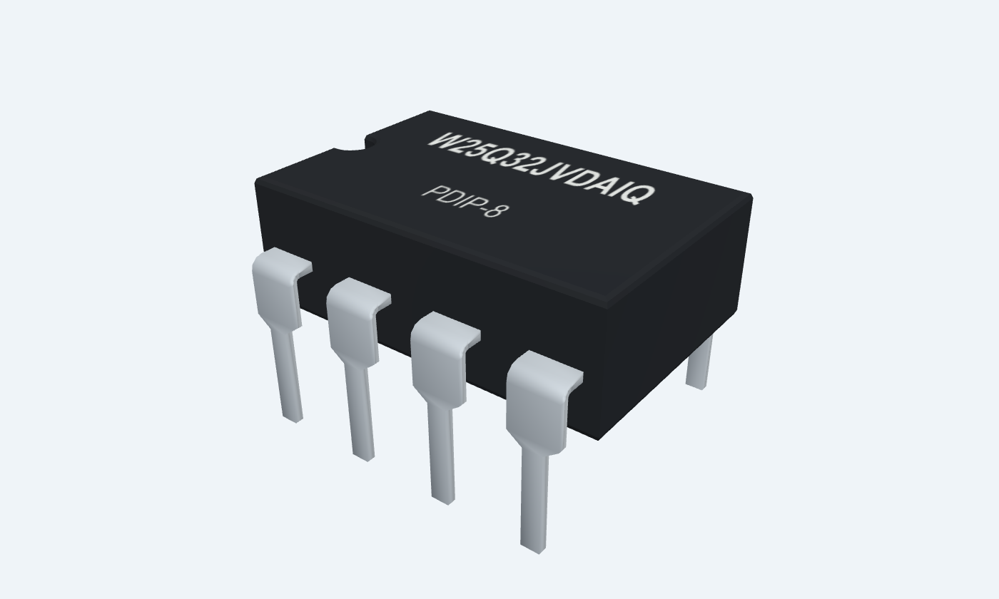
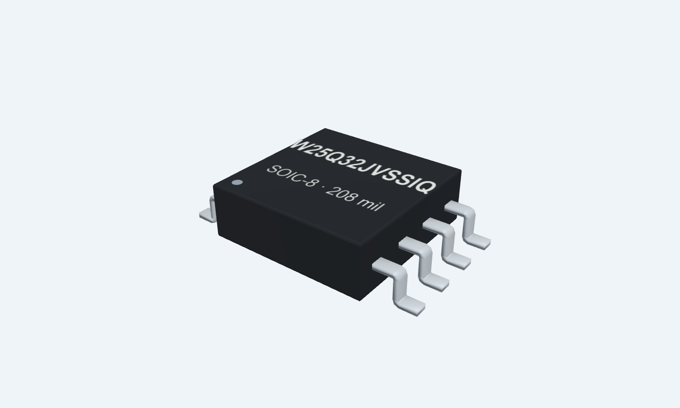
W25Q32JV is a 32-Mbit serial NOR flash memory, equivalent to 4 MiB of addressable storage. It retains data without power and supports standard, Dual and Quad SPI instructions. A controller supplies the clock and commands; the memory does not execute application code by itself. The array contains 16,384 pages of 256 bytes and 1,024 erasable 4 KiB sectors. Programming changes selected bits from one to zero, while an erase restores an entire sector or block to ones. Firmware must split page writes and preserve data that shares an erase unit. The views show the industrial Q-option PDIP-8 and 208-mil SOIC-8 packages from the referenced Winbond revision. Both operate at 2.7–3.6 V, with IO2 and IO3 reserved for quad transfers. The basic circuit uses 3.3 V standard SPI to read the JEDEC identification bytes EF 40 16 without altering memory.

8Physical pins
W25Q32JVDAIQPDIP-8
Manufacturer-referencedWinbond Electronics
Pin diagram
Select a pin to explore its connection
Highlight
W25Q32JVPDIP-8Top view
W25Q32JVSOIC-8 · 208 milTop view
Click a lead or use the arrow keys. Top view
PIN 1 · Serial control
Active-LOW select/CS
Function
Frames each serial command. HIGH deselects the chip and releases the data outputs.
How to connect
Connect to controller chip-select with a pull-up to 3.3 V; keep HIGH during power-up.
Electrical note
Program and erase commands must end on a complete byte boundary.
PIN 2 · Data lanes
Serial data output / quad I/ODO / IO1
Function
MISO in standard SPI; the second bidirectional lane in Dual/Quad operation.
How to connect
Connect to controller MISO in the example.
Electrical note
Output changes with the falling serial-clock edge.
PIN 3 · Data lanes
Quad data lane 2IO2
Function
Third bidirectional data signal for Quad SPI instructions in the selected JV Q ordering variant.
How to connect
Not used by the standard-SPI example; a 10 kΩ pull-up keeps the board net defined.
Electrical note
Do not relabel this selected part as /WP: the referenced IQ option starts with QE=1, enabling quad data; QE=0 selects /WP and /HOLD functions.
PIN 4 · Ground
GroundGND
Function
Supply and signal reference.
How to connect
Connect to the controller ground and bypass return.
PIN 5 · Data lanes
Serial data input / quad I/ODI / IO0
Function
MOSI in standard SPI; the first bidirectional lane in Dual/Quad operation.
How to connect
Connect controller MOSI to this pin.
Electrical note
Commands and standard input data are sampled on rising CLK edges, MSB first.
PIN 6 · Serial control
Serial clockCLK
Function
Clocks the selected SPI transaction.
How to connect
Use controller SCLK; the example uses mode 0 at 1 MHz.
Electrical note
Maximum permitted frequency depends on command and supply voltage.
PIN 7 · Data lanes
Quad data lane 3IO3
Function
Fourth bidirectional data signal for Quad SPI instructions.
How to connect
Unused by the standard-SPI example; 10 kΩ pull-up to 3.3 V.
Electrical note
This eight-lead package has no separate hardware /RESET pin.
PIN 8 · Supply
SupplyVCC
Function
Single 2.7–3.6 V supply.
How to connect
Use 3.3 V and a 100 nF bypass close to pins 8 and 4.
Electrical note
Not a 5 V device; use compatible controller levels.
Key specifications
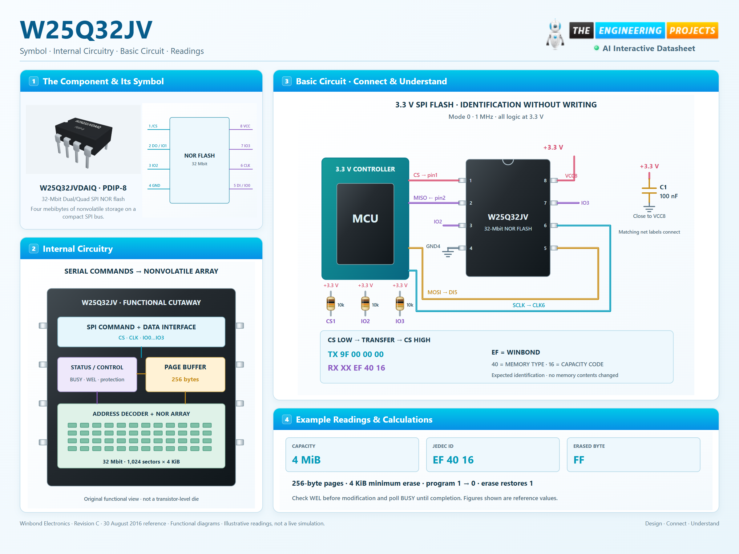
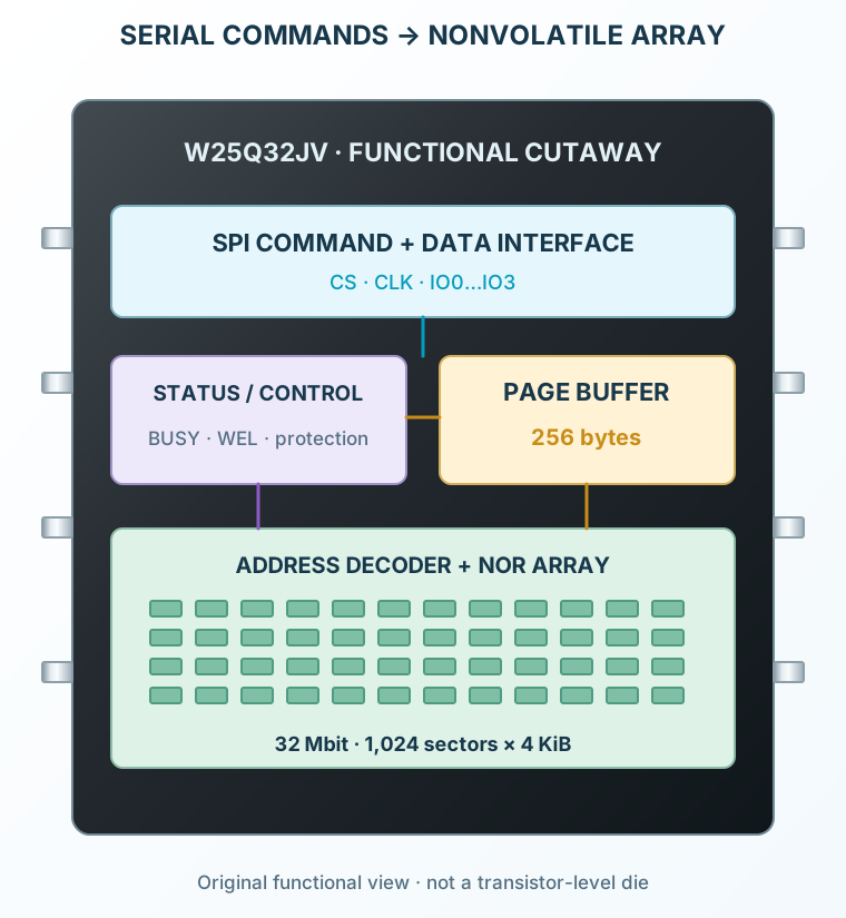
A serial command engine feeds address decoders, a page-program buffer and the NOR cell array. Status bits report whether an internal program or erase cycle is still busy.
Storage32 Mbit · 4 MiB
Supply range2.7–3.6 V
Program page256 bytes
Industrial ambient−40–85 °C
Package details
W25Q32JVDAIQ · PDIP-8
| Property | Details |
|---|---|
| Manufacturer | Winbond Electronics |
| Part number | W25Q32JVDAIQ |
| Package | PDIP-8 |
| Connections | 8 pins |
| Mounting | Through-hole |
| Lead pitch | 2.54 mm |
| Package code | PDIP-8 |
| Thermal reference | See operating and package limits |
Memory organization
Binary sizes, addresses and boundaries
Manufacturer specifications 8 parameters
Scroll sideways to see all columns.
| Parameter | Value | Conditions / notes |
|---|---|---|
| Capacity | 32 Mbit / 4,194,304 bytes | 4 MiB, not 32 megabytes |
| Address range | 0x000000–0x3FFFFF | 24-bit address field for normal array commands |
| Program page | 256 bytes | 16,384 pages |
| Sector erase | 4 KiB | 1,024 sectors |
| Block erase | 32 KiB or 64 KiB | 128 or 64 blocks respectively |
| Erased state | 0xFF per byte | All bits are ones |
| Programming direction | 1 → 0 | Erase required for 0 → 1 |
| Page boundary | Split writes before it | Excess program data wraps within the selected page |
No specifications match. Try a parameter name or a unit.
Plan data structures around erase units and power-loss recovery.
Common standard-SPI commands
MSB first; separate CS transaction for each command
Manufacturer specifications 11 parameters
Scroll sideways to see all columns.
| Parameter | Value | Conditions / notes |
|---|---|---|
| Read JEDEC identification | 9F | Returns EF 40 16 for the reviewed device |
| Read data | 03 + 24-bit address | No dummy byte; clock ceiling 50 MHz |
| Fast read | 0B + address + dummy byte | Observe supply-dependent fast-command limit |
| Write enable / disable | 06 / 04 | Sets / clears Write Enable Latch |
| Read status register 1 | 05 | BUSY bit0, WEL bit1 |
| Page program | 02 + address + data | 1…256 bytes, without crossing a page |
| Erase 4 KiB sector | 20 + address | Requires Write Enable |
| Erase 32 / 64 KiB block | 52 / D8 + address | Requires Write Enable |
| Chip erase | C7 or 60 | Erases the entire array |
| Power-down / release | B9 / AB | Observe entry and recovery timing |
| Software reset sequence | 66 then 99 | Two command frames; allow reset recovery |
No specifications match. Try a parameter name or a unit.
Identification and read commands do not modify user memory. Programming, erasing and protection writes do.
Supply, logic and startup
Revision C selected industrial variants
Manufacturer specifications 9 parameters
Scroll sideways to see all columns.
| Parameter | Value | Conditions / notes |
|---|---|---|
| Supply | 2.7–3.6 V | Example: regulated 3.3 V |
| Industrial ambient | −40 to +85°C | I temperature grade |
| Input HIGH / LOW | ≥0.7×VCC / ≤0.3×VCC | Not 5 V tolerant |
| Normal 03 read clock | Up to 50 MHz | At specified supply range |
| Other supported command clocks | Up to 133 MHz | VCC=3.0–3.6 V; not every framing mode has identical throughput |
| Fast-command clock at 2.7–3.0 V | Up to 104 MHz | Meet AC timing and loading requirements |
| VCC valid to CS LOW | 20 µs minimum | Keep CS HIGH during startup |
| Delay before write instruction | 5 ms minimum | After power becomes valid |
| Local bypass | 100 nF in the example | Short loop between VCC8 and GND4 |
No specifications match. Try a parameter name or a unit.
The 1 MHz identification example is intentionally well below the speed ceiling.
Program, erase and recovery times
Typical values and maximum completion limits
Manufacturer specifications 9 parameters
Scroll sideways to see all columns.
| Parameter | Value | Conditions / notes |
|---|---|---|
| Page program | 0.7 ms typical / 3 ms maximum | Poll BUSY rather than delaying only the typical time |
| 4 KiB sector erase | 45 ms typical / 400 ms maximum | Target erase unit only |
| 32 KiB block erase | 120 ms typical / 1.6 s maximum | Larger erase scope |
| 64 KiB block erase | 150 ms typical / 2 s maximum | Larger erase scope |
| Chip erase | 10 s typical / 50 s maximum | Entire memory |
| Write status register | 10 ms typical / 15 ms maximum | Protection/configuration operation |
| Power-down entry | 3 µs maximum | After CS rises for B9 |
| Release without ID read | 3 µs maximum | Wait before next instruction |
| Software-reset recovery | 30 µs minimum | Wait before next command |
No specifications match. Try a parameter name or a unit.
Retain supply throughout a modifying cycle; power interruption can leave the affected data incomplete.
Variant and package distinctions
Read the exact part suffix and revision
Manufacturer specifications 7 parameters
Scroll sideways to see all columns.
| Parameter | Value | Conditions / notes |
|---|---|---|
| Q ordering option | QE=1 factory default | QE is writable; Standard and Dual commands still available |
| Pin3 / pin7 | IO2 / IO3 | Quad data lanes; not /WP and /HOLD on this reference |
| Separate hardware RESET | Absent on these eight-lead packages | Available on specified larger packages |
| SOIC option shown | SS, 208-mil body | 5.28 × 5.28 mm nominal body |
| PDIP option shown | DA, 300-mil row format | 2.54 mm pitch |
| Other offered package families | VSOP, WSON, XSON, SOIC16, TFBGA | Not interchangeable footprints; not all displayed here |
| Orderability | Check current manufacturer/distributor listing | This page identifies the source revision and selected package definitions |
No specifications match. Try a parameter name or a unit.
Do not blindly substitute another W25Q32 family or suffix.
Read the device identity
3.3 V host, mode 0, 1 MHz
Manufacturer specifications 7 parameters
Scroll sideways to see all columns.
| Parameter | Value | Conditions / notes |
|---|---|---|
| Supply and ground | VCC8 / GND4 | 3.3 V / common ground |
| SPI signals | CS1, DO2, DI5, CLK6 | Host CS, MISO, MOSI, SCLK |
| Defined idle nets | 10 kΩ pull-ups on CS, IO2 and IO3 | IO2/IO3 unused by this standard-SPI example |
| Transmit bytes | 9F 00 00 00 | CS LOW for the complete transfer |
| Receive bytes | XX EF 40 16 | Discard response during opcode |
| After transfer | CS HIGH | Data output releases |
| Interpretation | EF: Winbond; 40: type; 16: capacity code | Expected identification, not a measured live result |
No specifications match. Try a parameter name or a unit.
All logic is 3.3 V. Add level translation if the controller uses incompatible voltages.
Connections by function
Select a pin for its function, connection guidance and electrical notes.
Serial control2 pins
Data lanes4 pins
Ground1 pin
Supply1 pin
Serial control2 pins
Data lanes4 pins
Ground1 pin
Supply1 pin
W25Q32JV at a glance
Follow the labeled connections and functional stages
How it works
3 stages · Explore one step at a time
Identify and address
The example sends 9F and reads manufacturer, memory-type and capacity identification bytes.
Read the stored data
03 followed by a 24-bit address reads bytes sequentially. Faster instructions use different framing and dummy cycles.
Update safely
Erase if needed, issue Write Enable for each modifying operation, program within a page and poll the status register.
Step 1 of 3
W25Q32JV in a circuit
A physical eight-lead package and a compatible 3.3 V controller.
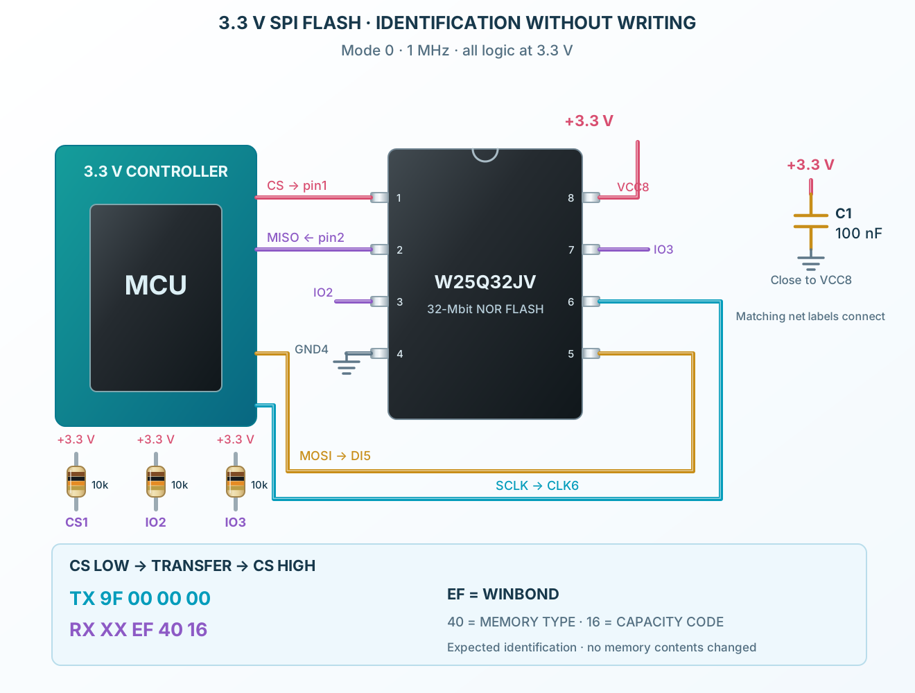
Connect it, step by step
Follow the component values and pin connections
Power and define idle state
Bypass VCC locally and keep CS HIGH through power-up.
Send the identification opcode
At 1 MHz mode0, transfer 9F and three dummy bytes under one CS LOW interval.
Read and deselect
Receive EF4016 after the opcode response, then raise CS.
Inside W25Q32JV
Serial control, addressing and page operations inside the package.
Explore the circuit
Select a stage to see its role and connections
Decode the command
CS and CLK frame opcodes, addresses and data.
Locate the memory
Address decoders select the array location or erase unit.
Manage internal cycles
Program and erase logic sets BUSY until the internal cycle finishes.
Selected packagePDIP-8W25Q32JVDAIQ
Physical connections8 pinsPackage-specific numbering
Reference collection7 tables51 parameters & pin functions
Pin reference
Signal names, electrical functions and connection guidance
Physical pin numbers8 pins
Scroll within the table to see all columns and rows.
| Pin | Signal | Type | Function & connection |
|---|---|---|---|
| /CS | Active-LOW select | Frames each serial command. HIGH deselects the chip and releases the data outputs.Connection guidanceConnect to controller chip-select with a pull-up to 3.3 V; keep HIGH during power-up. Program and erase commands must end on a complete byte boundary. | |
| DO / IO1 | Serial data output / quad I/O | MISO in standard SPI; the second bidirectional lane in Dual/Quad operation.Connection guidanceConnect to controller MISO in the example. Output changes with the falling serial-clock edge. | |
| IO2 | Quad data lane 2 | Third bidirectional data signal for Quad SPI instructions in the selected JV Q ordering variant.Connection guidanceNot used by the standard-SPI example; a 10 kΩ pull-up keeps the board net defined. Do not relabel this selected part as /WP: the referenced IQ option starts with QE=1, enabling quad data; QE=0 selects /WP and /HOLD functions. | |
| GND | Ground | Supply and signal reference.Connection guidanceConnect to the controller ground and bypass return. | |
| DI / IO0 | Serial data input / quad I/O | MOSI in standard SPI; the first bidirectional lane in Dual/Quad operation.Connection guidanceConnect controller MOSI to this pin. Commands and standard input data are sampled on rising CLK edges, MSB first. | |
| CLK | Serial clock | Clocks the selected SPI transaction.Connection guidanceUse controller SCLK; the example uses mode 0 at 1 MHz. Maximum permitted frequency depends on command and supply voltage. | |
| IO3 | Quad data lane 3 | Fourth bidirectional data signal for Quad SPI instructions.Connection guidanceUnused by the standard-SPI example; 10 kΩ pull-up to 3.3 V. This eight-lead package has no separate hardware /RESET pin. | |
| VCC | Supply | Single 2.7–3.6 V supply.Connection guidanceUse 3.3 V and a 100 nF bypass close to pins 8 and 4. Not a 5 V device; use compatible controller levels. |
No pins match these filters. Try another signal name or reset the filters.
Memory organization
Binary sizes, addresses and boundaries
Manufacturer-referenced values8 parameters
Scroll within the table to see all columns and rows.
| Parameter | Value | Conditions / notes |
|---|---|---|
| Capacity | 32 Mbit / 4,194,304 bytes | 4 MiB, not 32 megabytes |
| Address range | 0x000000–0x3FFFFF | 24-bit address field for normal array commands |
| Program page | 256 bytes | 16,384 pages |
| Sector erase | 4 KiB | 1,024 sectors |
| Block erase | 32 KiB or 64 KiB | 128 or 64 blocks respectively |
| Erased state | 0xFF per byte | All bits are ones |
| Programming direction | 1 → 0 | Erase required for 0 → 1 |
| Page boundary | Split writes before it | Excess program data wraps within the selected page |
No specifications match. Try a parameter name or a unit.
Plan data structures around erase units and power-loss recovery.
Common standard-SPI commands
MSB first; separate CS transaction for each command
Manufacturer-referenced values11 parameters
Scroll within the table to see all columns and rows.
| Parameter | Value | Conditions / notes |
|---|---|---|
| Read JEDEC identification | 9F | Returns EF 40 16 for the reviewed device |
| Read data | 03 + 24-bit address | No dummy byte; clock ceiling 50 MHz |
| Fast read | 0B + address + dummy byte | Observe supply-dependent fast-command limit |
| Write enable / disable | 06 / 04 | Sets / clears Write Enable Latch |
| Read status register 1 | 05 | BUSY bit0, WEL bit1 |
| Page program | 02 + address + data | 1…256 bytes, without crossing a page |
| Erase 4 KiB sector | 20 + address | Requires Write Enable |
| Erase 32 / 64 KiB block | 52 / D8 + address | Requires Write Enable |
| Chip erase | C7 or 60 | Erases the entire array |
| Power-down / release | B9 / AB | Observe entry and recovery timing |
| Software reset sequence | 66 then 99 | Two command frames; allow reset recovery |
No specifications match. Try a parameter name or a unit.
Identification and read commands do not modify user memory. Programming, erasing and protection writes do.
Supply, logic and startup
Revision C selected industrial variants
Manufacturer-referenced values9 parameters
Scroll within the table to see all columns and rows.
| Parameter | Value | Conditions / notes |
|---|---|---|
| Supply | 2.7–3.6 V | Example: regulated 3.3 V |
| Industrial ambient | −40 to +85°C | I temperature grade |
| Input HIGH / LOW | ≥0.7×VCC / ≤0.3×VCC | Not 5 V tolerant |
| Normal 03 read clock | Up to 50 MHz | At specified supply range |
| Other supported command clocks | Up to 133 MHz | VCC=3.0–3.6 V; not every framing mode has identical throughput |
| Fast-command clock at 2.7–3.0 V | Up to 104 MHz | Meet AC timing and loading requirements |
| VCC valid to CS LOW | 20 µs minimum | Keep CS HIGH during startup |
| Delay before write instruction | 5 ms minimum | After power becomes valid |
| Local bypass | 100 nF in the example | Short loop between VCC8 and GND4 |
No specifications match. Try a parameter name or a unit.
The 1 MHz identification example is intentionally well below the speed ceiling.
Program, erase and recovery times
Typical values and maximum completion limits
Manufacturer-referenced values9 parameters
Scroll within the table to see all columns and rows.
| Parameter | Value | Conditions / notes |
|---|---|---|
| Page program | 0.7 ms typical / 3 ms maximum | Poll BUSY rather than delaying only the typical time |
| 4 KiB sector erase | 45 ms typical / 400 ms maximum | Target erase unit only |
| 32 KiB block erase | 120 ms typical / 1.6 s maximum | Larger erase scope |
| 64 KiB block erase | 150 ms typical / 2 s maximum | Larger erase scope |
| Chip erase | 10 s typical / 50 s maximum | Entire memory |
| Write status register | 10 ms typical / 15 ms maximum | Protection/configuration operation |
| Power-down entry | 3 µs maximum | After CS rises for B9 |
| Release without ID read | 3 µs maximum | Wait before next instruction |
| Software-reset recovery | 30 µs minimum | Wait before next command |
No specifications match. Try a parameter name or a unit.
Retain supply throughout a modifying cycle; power interruption can leave the affected data incomplete.
Variant and package distinctions
Read the exact part suffix and revision
Manufacturer-referenced values7 parameters
Scroll within the table to see all columns and rows.
| Parameter | Value | Conditions / notes |
|---|---|---|
| Q ordering option | QE=1 factory default | QE is writable; Standard and Dual commands still available |
| Pin3 / pin7 | IO2 / IO3 | Quad data lanes; not /WP and /HOLD on this reference |
| Separate hardware RESET | Absent on these eight-lead packages | Available on specified larger packages |
| SOIC option shown | SS, 208-mil body | 5.28 × 5.28 mm nominal body |
| PDIP option shown | DA, 300-mil row format | 2.54 mm pitch |
| Other offered package families | VSOP, WSON, XSON, SOIC16, TFBGA | Not interchangeable footprints; not all displayed here |
| Orderability | Check current manufacturer/distributor listing | This page identifies the source revision and selected package definitions |
No specifications match. Try a parameter name or a unit.
Do not blindly substitute another W25Q32 family or suffix.
Read the device identity
3.3 V host, mode 0, 1 MHz
Manufacturer-referenced values7 parameters
Scroll within the table to see all columns and rows.
| Parameter | Value | Conditions / notes |
|---|---|---|
| Supply and ground | VCC8 / GND4 | 3.3 V / common ground |
| SPI signals | CS1, DO2, DI5, CLK6 | Host CS, MISO, MOSI, SCLK |
| Defined idle nets | 10 kΩ pull-ups on CS, IO2 and IO3 | IO2/IO3 unused by this standard-SPI example |
| Transmit bytes | 9F 00 00 00 | CS LOW for the complete transfer |
| Receive bytes | XX EF 40 16 | Discard response during opcode |
| After transfer | CS HIGH | Data output releases |
| Interpretation | EF: Winbond; 40: type; 16: capacity code | Expected identification, not a measured live result |
No specifications match. Try a parameter name or a unit.
All logic is 3.3 V. Add level translation if the controller uses incompatible voltages.
No matching rowsTry a pin name, parameter, unit or test condition, or reset the filters.
Firmware storage
Hold executable images that the host reads or maps through a suitable controller.
Manufacturer application guideGraphics and audio assets
Store larger resources outside MCU internal flash.
Manufacturer application guidePersistent logs and settings
Use wear management, erase-unit planning and power-loss-safe record formats.
Manufacturer application guideTake it into ProTech
Find W25Q32JV in the Components Library to place its schematic symbol and connect its pins.
Reference page · circuit simulation model not yet availableOpen ProTech