 BETA
Decode the command
CS and CLK frame opcodes, addresses and data.
Explore the internal circuitry and functional stages of W25Q32JV.
Serial control, addressing and page operations inside the package.
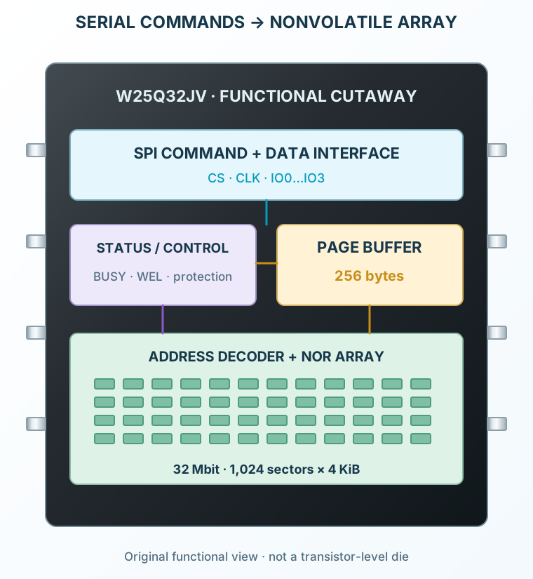
Select a stage to see its role and connections
CS and CLK frame opcodes, addresses and data.
Address decoders select the array location or erase unit.
Program and erase logic sets BUSY until the internal cycle finishes.