 BETA
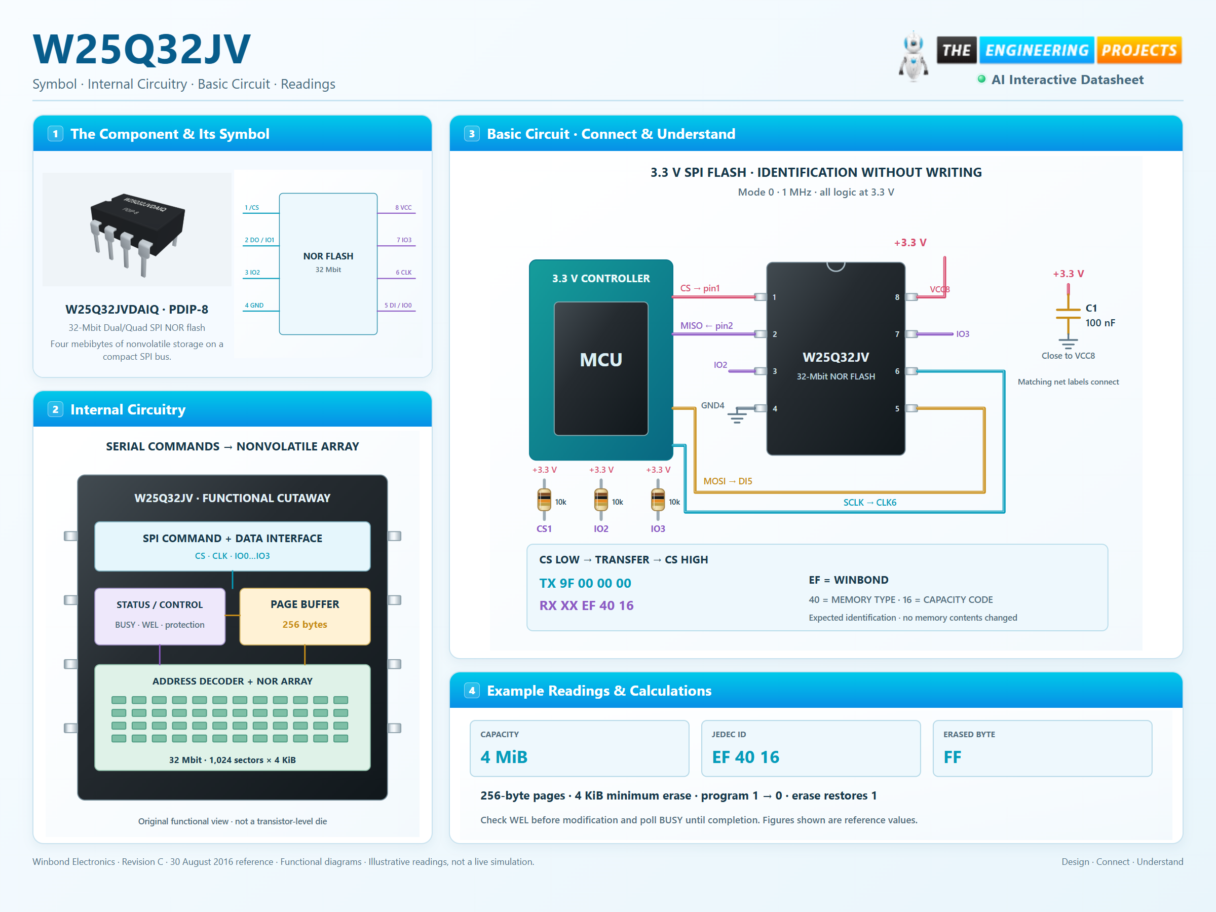
32-Mbit Dual/Quad SPI NOR flash
W25Q32JV Working Principle
Learn how W25Q32JV works with an illustrated explanation and practical readings.
Package view
W25Q32JV at a glance
Follow the labeled connections and functional stages
How it works
3 stages · Explore one step at a time
Identify and address
The example sends 9F and reads manufacturer, memory-type and capacity identification bytes.
Read the stored data
03 followed by a 24-bit address reads bytes sequentially. Faster instructions use different framing and dummy cycles.
Update safely
Erase if needed, issue Write Enable for each modifying operation, program within a page and poll the status register.
Step 1 of 3