 BETA
Power and define idle state
Bypass VCC locally and keep CS HIGH through power-up.
Build a basic W25Q32JV circuit with labeled pins, component values and connection guidance.
A physical eight-lead package and a compatible 3.3 V controller.
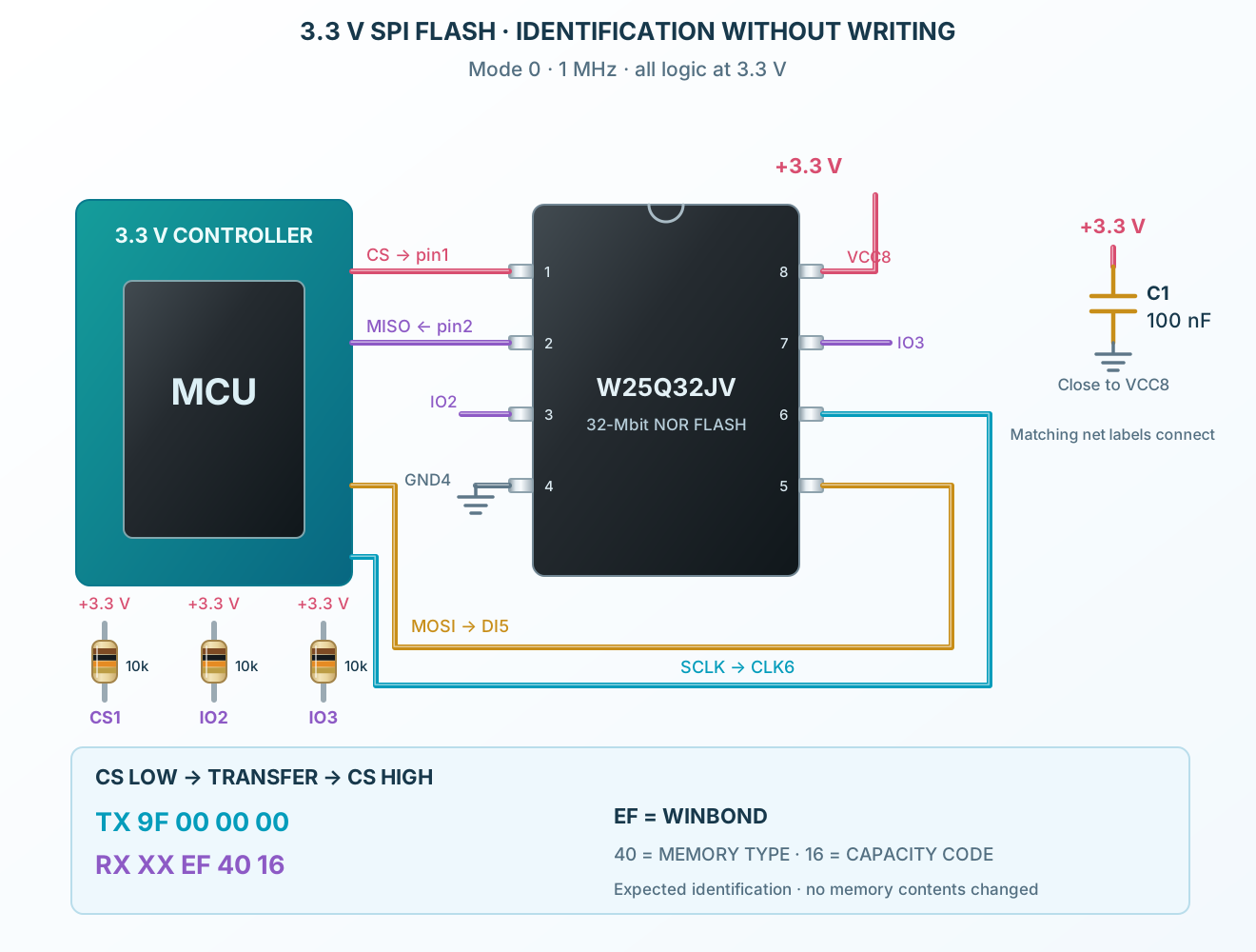
Follow the component values and pin connections
Bypass VCC locally and keep CS HIGH through power-up.
At 1 MHz mode0, transfer 9F and three dummy bytes under one CS LOW interval.
Receive EF4016 after the opcode response, then raise CS.