PIC18F45208-bit PIC18 microcontroller with 40/44-pin packages
More memory, flexible clocks and carefully shared peripheral pins.
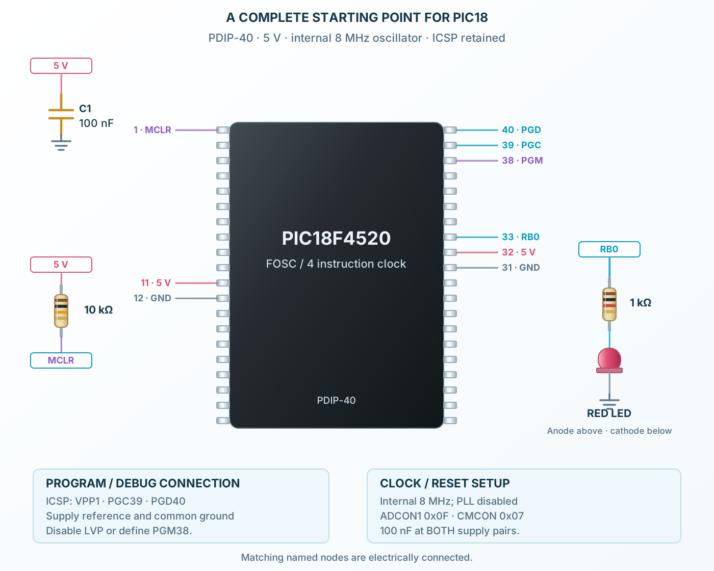
PIC18F4520 is an eight-bit microcontroller with 32 KB of Flash program memory, 1536 bytes of RAM and 256 bytes of data EEPROM. Its PIC18 core adds an eight-by-eight hardware multiplier, interrupt priorities and output latch registers. Up to 36 I/O lines share connections with timers, communication interfaces and a thirteen-channel ADC. The selected F-device operates from 4.2 to 5.5 V; the LF variant has different low-voltage limits. An internal oscillator can supply 31 kHz through 8 MHz, with a PLL option for higher internal-clock operation. A 40 MHz external oscillator gives up to 10 million instruction cycles per second because the instruction clock is FOSC divided by four. The reference circuit uses regulated 5 V, the internal 8 MHz oscillator, both supply pairs, ICSP and a resistor-limited LED on RB0. Firmware must disable unwanted analog functions and configure latches, direction and clock selection. PDIP and TQFP use different physical pin numbers, which the package selector keeps mapped consistently.
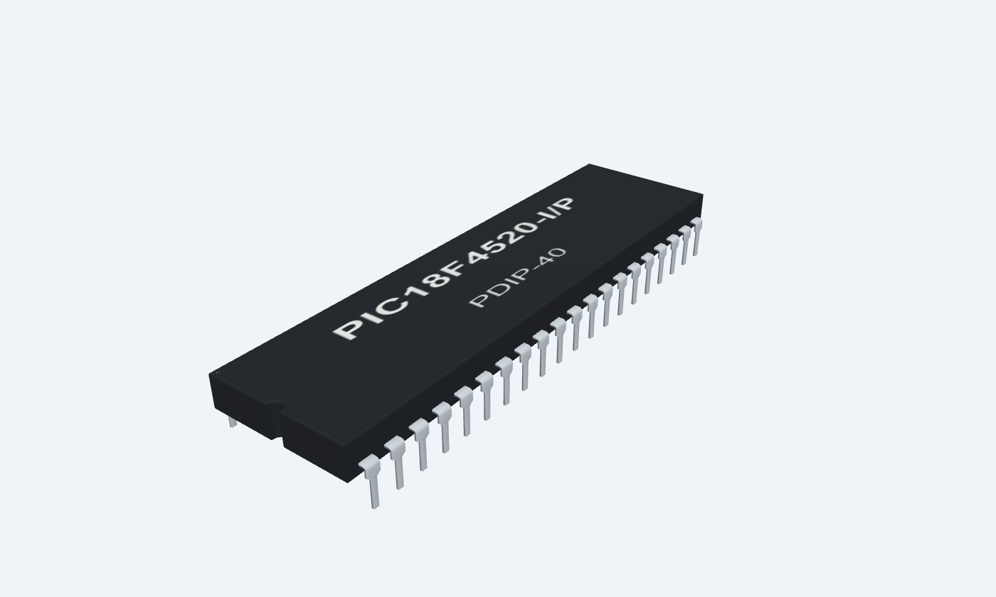
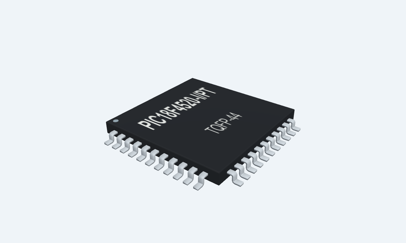

Reset and programmingAnalog / digital multiplexingPorts and serial peripheralsConnect every supply pinOscillator or digital I/OUnused TQFP leads
PIC18F4520PDIP-40Top view
PIC18F4520TQFP-44Top view
Click a lead or use the arrow keys. Top view
PIN 1 · Reset and programming
Reset / programmingMCLR / VPP / RE3
Function
Active-low reset and programming voltage input; RE3 is input-only when MCLR is disabled.
How to connect
10 kΩ pull-up to 5 V; preserve ICSP VPP access.
PIN 2 · Analog / digital multiplexing
GPIO / peripheralRA0 / AN0
Function
Multiplexed port and named peripheral functions. Set direction, analog selection and peripheral routing explicitly.
How to connect
Use supply-compatible signals and define unused inputs.
Electrical note
ADCON1 selects analog/digital functions; AN8–AN12 are on PORTB.
PIN 3 · Analog / digital multiplexing
GPIO / peripheralRA1 / AN1
Function
Multiplexed port and named peripheral functions. Set direction, analog selection and peripheral routing explicitly.
How to connect
Use supply-compatible signals and define unused inputs.
Electrical note
ADCON1 selects analog/digital functions; AN8–AN12 are on PORTB.
PIN 4 · Analog / digital multiplexing
GPIO / peripheralRA2 / AN2 / VREF− / CVREF
Function
Multiplexed port and named peripheral functions. Set direction, analog selection and peripheral routing explicitly.
How to connect
Use supply-compatible signals and define unused inputs.
Electrical note
ADCON1 selects analog/digital functions; AN8–AN12 are on PORTB.
PIN 5 · Analog / digital multiplexing
GPIO / peripheralRA3 / AN3 / VREF+
Function
Multiplexed port and named peripheral functions. Set direction, analog selection and peripheral routing explicitly.
How to connect
Use supply-compatible signals and define unused inputs.
Electrical note
ADCON1 selects analog/digital functions; AN8–AN12 are on PORTB.
PIN 6 · Ports and serial peripherals
GPIO / peripheralRA4 / T0CKI / C1OUT
Function
Multiplexed port and named peripheral functions. Set direction, analog selection and peripheral routing explicitly.
How to connect
Use supply-compatible signals and define unused inputs.
PIN 7 · Analog / digital multiplexing
GPIO / peripheralRA5 / AN4 / SS / HLVDIN / C2OUT
Function
Multiplexed port and named peripheral functions. Set direction, analog selection and peripheral routing explicitly.
How to connect
Use supply-compatible signals and define unused inputs.
Electrical note
ADCON1 selects analog/digital functions; AN8–AN12 are on PORTB.
PIN 8 · Analog / digital multiplexing
GPIO / peripheralRE0 / RD / AN5
Function
Multiplexed port and named peripheral functions. Set direction, analog selection and peripheral routing explicitly.
How to connect
Use supply-compatible signals and define unused inputs.
Electrical note
ADCON1 selects analog/digital functions; AN8–AN12 are on PORTB.
PIN 9 · Analog / digital multiplexing
GPIO / peripheralRE1 / WR / AN6
Function
Multiplexed port and named peripheral functions. Set direction, analog selection and peripheral routing explicitly.
How to connect
Use supply-compatible signals and define unused inputs.
Electrical note
ADCON1 selects analog/digital functions; AN8–AN12 are on PORTB.
PIN 10 · Analog / digital multiplexing
GPIO / peripheralRE2 / CS / AN7
Function
Multiplexed port and named peripheral functions. Set direction, analog selection and peripheral routing explicitly.
How to connect
Use supply-compatible signals and define unused inputs.
Electrical note
ADCON1 selects analog/digital functions; AN8–AN12 are on PORTB.
PIN 11 · Connect every supply pin
SupplyVDD
Function
Positive supply; connect both VDD pins.
How to connect
Regulated 5 V with a local 100 nF capacitor to VSS.
PIN 12 · Connect every supply pin
SupplyVSS
Function
Ground return; connect both VSS pins.
How to connect
Common ground plane.
PIN 13 · Oscillator or digital I/O
Oscillator / GPIOOSC1 / CLKI / RA7
Function
External oscillator or GPIO, depending on the oscillator configuration.
How to connect
The internal 8 MHz example leaves these available as RA7 / RA6 with the matching configuration.
PIN 14 · Oscillator or digital I/O
Oscillator / GPIOOSC2 / CLKO / RA6
Function
External oscillator or GPIO, depending on the oscillator configuration.
How to connect
The internal 8 MHz example leaves these available as RA7 / RA6 with the matching configuration.
PIN 15 · Ports and serial peripherals
GPIO / peripheralRC0 / T1OSO / T13CKI
Function
Multiplexed port and named peripheral functions. Set direction, analog selection and peripheral routing explicitly.
How to connect
Use supply-compatible signals and define unused inputs.
PIN 16 · Ports and serial peripherals
GPIO / peripheralRC1 / T1OSI / CCP2
Function
Multiplexed port and named peripheral functions. Set direction, analog selection and peripheral routing explicitly.
How to connect
Use supply-compatible signals and define unused inputs.
Electrical note
CCP2MX selects RC1 or RB3 for CCP2.
PIN 17 · Ports and serial peripherals
GPIO / peripheralRC2 / CCP1 / P1A
Function
Multiplexed port and named peripheral functions. Set direction, analog selection and peripheral routing explicitly.
How to connect
Use supply-compatible signals and define unused inputs.
PIN 18 · Ports and serial peripherals
GPIO / peripheralRC3 / SCK / SCL
Function
Multiplexed port and named peripheral functions. Set direction, analog selection and peripheral routing explicitly.
How to connect
Use supply-compatible signals and define unused inputs.
PIN 19 · Ports and serial peripherals
GPIO / peripheralRD0 / PSP0
Function
Multiplexed port and named peripheral functions. Set direction, analog selection and peripheral routing explicitly.
How to connect
Use supply-compatible signals and define unused inputs.
PIN 20 · Ports and serial peripherals
GPIO / peripheralRD1 / PSP1
Function
Multiplexed port and named peripheral functions. Set direction, analog selection and peripheral routing explicitly.
How to connect
Use supply-compatible signals and define unused inputs.
PIN 21 · Ports and serial peripherals
GPIO / peripheralRD2 / PSP2
Function
Multiplexed port and named peripheral functions. Set direction, analog selection and peripheral routing explicitly.
How to connect
Use supply-compatible signals and define unused inputs.
PIN 22 · Ports and serial peripherals
GPIO / peripheralRD3 / PSP3
Function
Multiplexed port and named peripheral functions. Set direction, analog selection and peripheral routing explicitly.
How to connect
Use supply-compatible signals and define unused inputs.
PIN 23 · Ports and serial peripherals
GPIO / peripheralRC4 / SDI / SDA
Function
Multiplexed port and named peripheral functions. Set direction, analog selection and peripheral routing explicitly.
How to connect
Use supply-compatible signals and define unused inputs.
PIN 24 · Ports and serial peripherals
GPIO / peripheralRC5 / SDO
Function
Multiplexed port and named peripheral functions. Set direction, analog selection and peripheral routing explicitly.
How to connect
Use supply-compatible signals and define unused inputs.
PIN 25 · Ports and serial peripherals
GPIO / peripheralRC6 / TX / CK
Function
Multiplexed port and named peripheral functions. Set direction, analog selection and peripheral routing explicitly.
How to connect
Use supply-compatible signals and define unused inputs.
PIN 26 · Ports and serial peripherals
GPIO / peripheralRC7 / RX / DT
Function
Multiplexed port and named peripheral functions. Set direction, analog selection and peripheral routing explicitly.
How to connect
Use supply-compatible signals and define unused inputs.
PIN 27 · Ports and serial peripherals
GPIO / peripheralRD4 / PSP4
Function
Multiplexed port and named peripheral functions. Set direction, analog selection and peripheral routing explicitly.
How to connect
Use supply-compatible signals and define unused inputs.
PIN 28 · Ports and serial peripherals
GPIO / peripheralRD5 / PSP5 / P1B
Function
Multiplexed port and named peripheral functions. Set direction, analog selection and peripheral routing explicitly.
How to connect
Use supply-compatible signals and define unused inputs.
PIN 29 · Ports and serial peripherals
GPIO / peripheralRD6 / PSP6 / P1C
Function
Multiplexed port and named peripheral functions. Set direction, analog selection and peripheral routing explicitly.
How to connect
Use supply-compatible signals and define unused inputs.
PIN 30 · Ports and serial peripherals
GPIO / peripheralRD7 / PSP7 / P1D
Function
Multiplexed port and named peripheral functions. Set direction, analog selection and peripheral routing explicitly.
How to connect
Use supply-compatible signals and define unused inputs.
PIN 31 · Connect every supply pin
SupplyVSS
Function
Ground return; connect both VSS pins.
How to connect
Common ground plane.
PIN 32 · Connect every supply pin
SupplyVDD
Function
Positive supply; connect both VDD pins.
How to connect
Regulated 5 V with a local 100 nF capacitor to VSS.
PIN 33 · Analog / digital multiplexing
GPIO / peripheralRB0 / INT0 / FLT0 / AN12
Function
Multiplexed port and named peripheral functions. Set direction, analog selection and peripheral routing explicitly.
How to connect
Example: RB0 through 1 kΩ and a red LED to ground.
Electrical note
ADCON1 selects analog/digital functions; AN8–AN12 are on PORTB.
PIN 34 · Analog / digital multiplexing
GPIO / peripheralRB1 / INT1 / AN10
Function
Multiplexed port and named peripheral functions. Set direction, analog selection and peripheral routing explicitly.
How to connect
Use supply-compatible signals and define unused inputs.
Electrical note
ADCON1 selects analog/digital functions; AN8–AN12 are on PORTB.
PIN 35 · Analog / digital multiplexing
GPIO / peripheralRB2 / INT2 / AN8
Function
Multiplexed port and named peripheral functions. Set direction, analog selection and peripheral routing explicitly.
How to connect
Use supply-compatible signals and define unused inputs.
Electrical note
ADCON1 selects analog/digital functions; AN8–AN12 are on PORTB.
PIN 36 · Analog / digital multiplexing
GPIO / peripheralRB3 / AN9 / CCP2
Function
Multiplexed port and named peripheral functions. Set direction, analog selection and peripheral routing explicitly.
How to connect
Use supply-compatible signals and define unused inputs.
Electrical note
CCP2 on RB3 is the alternate CCP2MX routing.
PIN 37 · Analog / digital multiplexing
GPIO / peripheralRB4 / KBI0 / AN11
Function
Multiplexed port and named peripheral functions. Set direction, analog selection and peripheral routing explicitly.
How to connect
Use supply-compatible signals and define unused inputs.
Electrical note
ADCON1 selects analog/digital functions; AN8–AN12 are on PORTB.
PIN 38 · Ports and serial peripherals
GPIO / peripheralRB5 / KBI1 / PGM
Function
Multiplexed port and named peripheral functions. Set direction, analog selection and peripheral routing explicitly.
How to connect
Use supply-compatible signals and define unused inputs.
Electrical note
RB5 is PGM when low-voltage programming is enabled; define it or deliberately disable LVP.
PIN 39 · Ports and serial peripherals
GPIO / peripheralRB6 / KBI2 / PGC
Function
Multiplexed port and named peripheral functions. Set direction, analog selection and peripheral routing explicitly.
How to connect
Connect to ICSP programmer with VPP, VDD and VSS.
PIN 40 · Ports and serial peripherals
GPIO / peripheralRB7 / KBI3 / PGD
Function
Multiplexed port and named peripheral functions. Set direction, analog selection and peripheral routing explicitly.
How to connect
Connect to ICSP programmer with VPP, VDD and VSS.
PIN 41 · Unused TQFP leads
No connectionNC
Function
Unused physical lead in the TQFP package.
How to connect
Leave unconnected.
PIN 42 · Unused TQFP leads
No connectionNC
Function
Unused physical lead in the TQFP package.
How to connect
Leave unconnected.
PIN 43 · Unused TQFP leads
No connectionNC
Function
Unused physical lead in the TQFP package.
How to connect
Leave unconnected.
PIN 44 · Unused TQFP leads
No connectionNC
Function
Unused physical lead in the TQFP package.
How to connect
Leave unconnected.
At a glance
8-bit PIC18 microcontroller with 40/44-pin packages
Ports share analog, timing and communication functions; the selected configuration determines which function reaches each pad.
32 KBProgram Flash
1536 bytesData RAM
40 MHzMaximum FOSC
10-bit 13 inputsADC
Operating profile
PIC18F4520-I/P
CPU and memory
Key parameters and their test conditions
- Program Flash
- 32 KBConditions / notes: 16K 16-bit words; some instructions occupy two words
- Data RAM
- 1536 bytesConditions / notes: Access-bank and banked addressing
- Data EEPROM
- 256 bytesConditions / notes: Nonvolatile application storage
- Hardware multiplier
- 8 × 8 bitsConditions / notes: Single instruction cycle multiply
- Return stack
- 31 levelsConditions / notes: Hardware return-address stack
- Instruction clock
- FOSC / 4Conditions / notes: Up to 10 MIPS at 40 MHz
Package details
Follows the selected physical package
- Manufacturer
- Microchip Technology
- Part number
- PIC18F4520-I/P
- Package
- PDIP-40
- Connections
- 40 pins
- Mounting
- Through-hole
- Lead pitch
- 2.54 mm
- Package code
- PDIP-40
- Thermal reference
- See operating and package limits
Connections by function
Select a pin to open its function, electrical notes and wiring guidance.
Reset and programming1 pins
Analog / digital multiplexing13 pins
Ports and serial peripherals20 pins
Connect every supply pin4 pins
Oscillator or digital I/O2 pins
Ports and serial peripherals20 pins
Connect every supply pin4 pins
Analog / digital multiplexing13 pins
Unused TQFP leads4 pins
Reset and programming1 pins
Oscillator or digital I/O2 pins
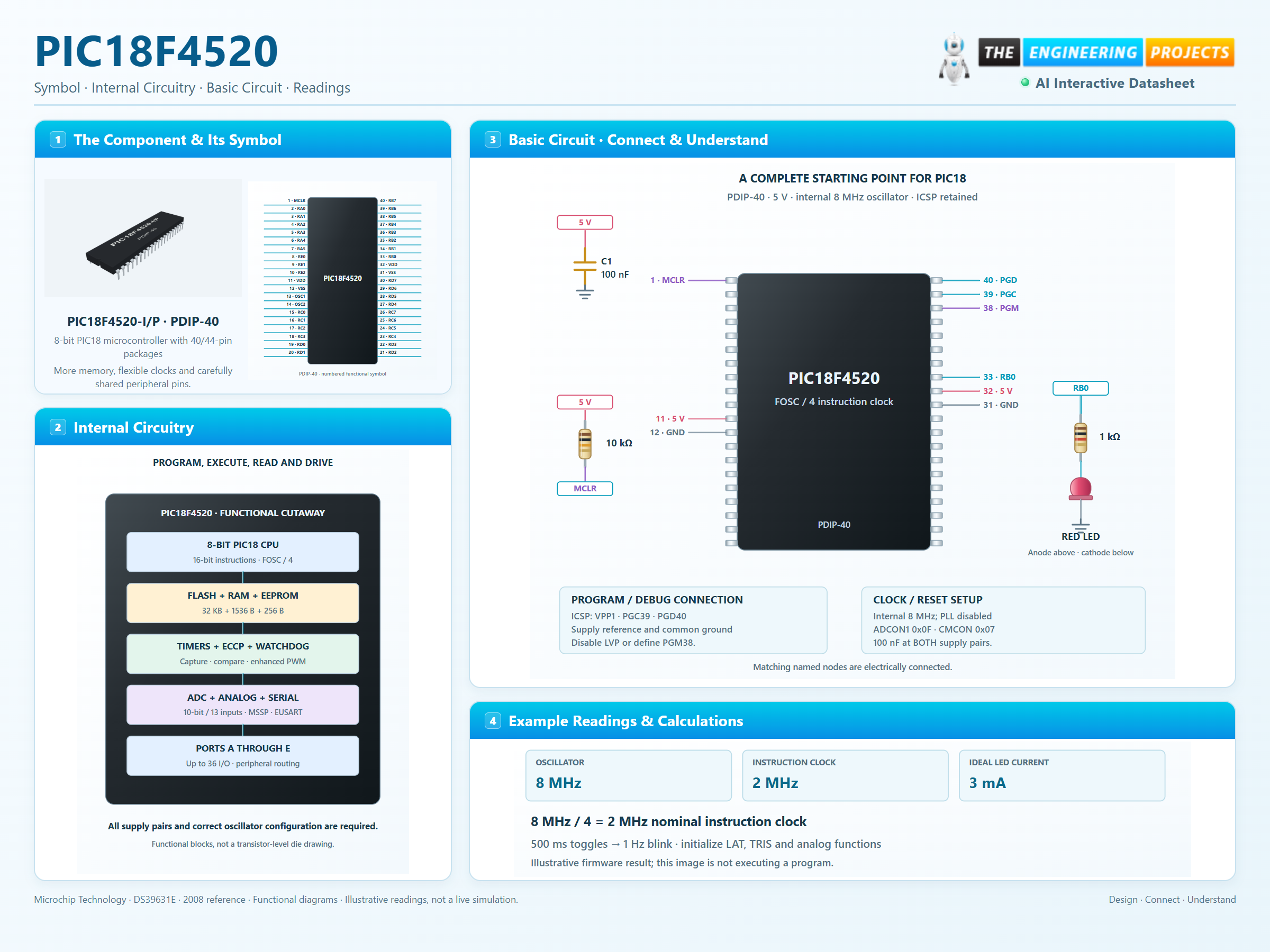
Power every pair
Connect both VDD and VSS pairs with nearby bypass capacitors.
Choose the clock
Select the internal oscillator and its 8 MHz setting.
Configure the ports
Set analog functions, output latches and direction before running the example.
The 8 MHz internal-clock example has a nominal 2 MHz instruction clock. Toggle every 500 ms for a 1 Hz full blink cycle.
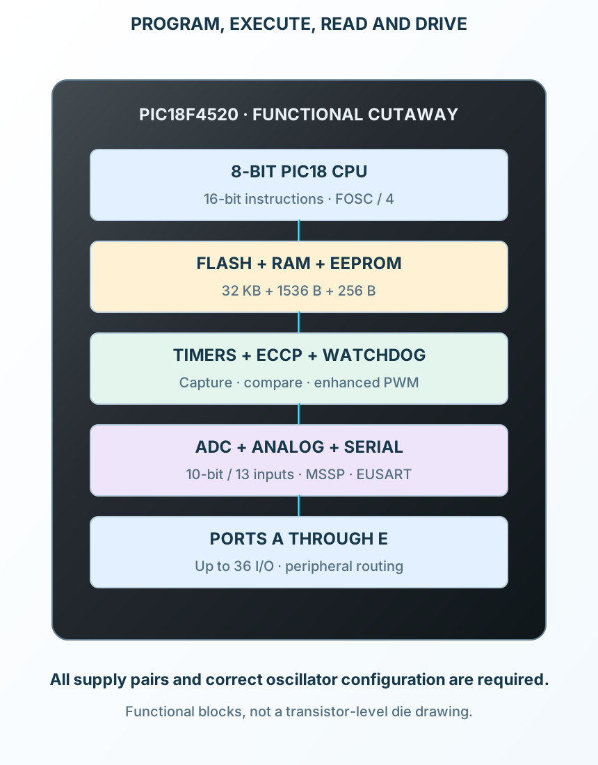
Pin reference
Select a pin to explore its function and connection.
40 pins
| Pin | Signal | Type | Function |
|---|---|---|---|
| MCLR / VPP / RE3 | Reset / programming | Active-low reset and programming voltage input; RE3 is input-only when MCLR is disabled. | |
| RA0 / AN0 | GPIO / peripheral | Multiplexed port and named peripheral functions. Set direction, analog selection and peripheral routing explicitly. | |
| RA1 / AN1 | GPIO / peripheral | Multiplexed port and named peripheral functions. Set direction, analog selection and peripheral routing explicitly. | |
| RA2 / AN2 / VREF− / CVREF | GPIO / peripheral | Multiplexed port and named peripheral functions. Set direction, analog selection and peripheral routing explicitly. | |
| RA3 / AN3 / VREF+ | GPIO / peripheral | Multiplexed port and named peripheral functions. Set direction, analog selection and peripheral routing explicitly. | |
| RA4 / T0CKI / C1OUT | GPIO / peripheral | Multiplexed port and named peripheral functions. Set direction, analog selection and peripheral routing explicitly. | |
| RA5 / AN4 / SS / HLVDIN / C2OUT | GPIO / peripheral | Multiplexed port and named peripheral functions. Set direction, analog selection and peripheral routing explicitly. | |
| RE0 / RD / AN5 | GPIO / peripheral | Multiplexed port and named peripheral functions. Set direction, analog selection and peripheral routing explicitly. | |
| RE1 / WR / AN6 | GPIO / peripheral | Multiplexed port and named peripheral functions. Set direction, analog selection and peripheral routing explicitly. | |
| RE2 / CS / AN7 | GPIO / peripheral | Multiplexed port and named peripheral functions. Set direction, analog selection and peripheral routing explicitly. | |
| VDD | Supply | Positive supply; connect both VDD pins. | |
| VSS | Supply | Ground return; connect both VSS pins. | |
| OSC1 / CLKI / RA7 | Oscillator / GPIO | External oscillator or GPIO, depending on the oscillator configuration. | |
| OSC2 / CLKO / RA6 | Oscillator / GPIO | External oscillator or GPIO, depending on the oscillator configuration. | |
| RC0 / T1OSO / T13CKI | GPIO / peripheral | Multiplexed port and named peripheral functions. Set direction, analog selection and peripheral routing explicitly. | |
| RC1 / T1OSI / CCP2 | GPIO / peripheral | Multiplexed port and named peripheral functions. Set direction, analog selection and peripheral routing explicitly. | |
| RC2 / CCP1 / P1A | GPIO / peripheral | Multiplexed port and named peripheral functions. Set direction, analog selection and peripheral routing explicitly. | |
| RC3 / SCK / SCL | GPIO / peripheral | Multiplexed port and named peripheral functions. Set direction, analog selection and peripheral routing explicitly. | |
| RD0 / PSP0 | GPIO / peripheral | Multiplexed port and named peripheral functions. Set direction, analog selection and peripheral routing explicitly. | |
| RD1 / PSP1 | GPIO / peripheral | Multiplexed port and named peripheral functions. Set direction, analog selection and peripheral routing explicitly. | |
| RD2 / PSP2 | GPIO / peripheral | Multiplexed port and named peripheral functions. Set direction, analog selection and peripheral routing explicitly. | |
| RD3 / PSP3 | GPIO / peripheral | Multiplexed port and named peripheral functions. Set direction, analog selection and peripheral routing explicitly. | |
| RC4 / SDI / SDA | GPIO / peripheral | Multiplexed port and named peripheral functions. Set direction, analog selection and peripheral routing explicitly. | |
| RC5 / SDO | GPIO / peripheral | Multiplexed port and named peripheral functions. Set direction, analog selection and peripheral routing explicitly. | |
| RC6 / TX / CK | GPIO / peripheral | Multiplexed port and named peripheral functions. Set direction, analog selection and peripheral routing explicitly. | |
| RC7 / RX / DT | GPIO / peripheral | Multiplexed port and named peripheral functions. Set direction, analog selection and peripheral routing explicitly. | |
| RD4 / PSP4 | GPIO / peripheral | Multiplexed port and named peripheral functions. Set direction, analog selection and peripheral routing explicitly. | |
| RD5 / PSP5 / P1B | GPIO / peripheral | Multiplexed port and named peripheral functions. Set direction, analog selection and peripheral routing explicitly. | |
| RD6 / PSP6 / P1C | GPIO / peripheral | Multiplexed port and named peripheral functions. Set direction, analog selection and peripheral routing explicitly. | |
| RD7 / PSP7 / P1D | GPIO / peripheral | Multiplexed port and named peripheral functions. Set direction, analog selection and peripheral routing explicitly. | |
| VSS | Supply | Ground return; connect both VSS pins. | |
| VDD | Supply | Positive supply; connect both VDD pins. | |
| RB0 / INT0 / FLT0 / AN12 | GPIO / peripheral | Multiplexed port and named peripheral functions. Set direction, analog selection and peripheral routing explicitly. | |
| RB1 / INT1 / AN10 | GPIO / peripheral | Multiplexed port and named peripheral functions. Set direction, analog selection and peripheral routing explicitly. | |
| RB2 / INT2 / AN8 | GPIO / peripheral | Multiplexed port and named peripheral functions. Set direction, analog selection and peripheral routing explicitly. | |
| RB3 / AN9 / CCP2 | GPIO / peripheral | Multiplexed port and named peripheral functions. Set direction, analog selection and peripheral routing explicitly. | |
| RB4 / KBI0 / AN11 | GPIO / peripheral | Multiplexed port and named peripheral functions. Set direction, analog selection and peripheral routing explicitly. | |
| RB5 / KBI1 / PGM | GPIO / peripheral | Multiplexed port and named peripheral functions. Set direction, analog selection and peripheral routing explicitly. | |
| RB6 / KBI2 / PGC | GPIO / peripheral | Multiplexed port and named peripheral functions. Set direction, analog selection and peripheral routing explicitly. | |
| RB7 / KBI3 / PGD | GPIO / peripheral | Multiplexed port and named peripheral functions. Set direction, analog selection and peripheral routing explicitly. | |
| NC | No connection | Unused physical lead in the TQFP package. | |
| NC | No connection | Unused physical lead in the TQFP package. | |
| NC | No connection | Unused physical lead in the TQFP package. | |
| NC | No connection | Unused physical lead in the TQFP package. |
No pins match. Try a signal name or choose All pins.
CPU and memory
Selected PIC18F4520
Manufacturer specifications 6 parameters
| Parameter | Value | Conditions / notes |
|---|---|---|
| Program Flash | 32 KB | 16K 16-bit words; some instructions occupy two words |
| Data RAM | 1536 bytes | Access-bank and banked addressing |
| Data EEPROM | 256 bytes | Nonvolatile application storage |
| Hardware multiplier | 8 × 8 bits | Single instruction cycle multiply |
| Return stack | 31 levels | Hardware return-address stack |
| Instruction clock | FOSC / 4 | Up to 10 MIPS at 40 MHz |
No specifications match. Try a parameter name or a unit.
Instruction timing and branch costs still matter in software delays.
Supply and reset
F-device industrial selection
Manufacturer specifications 6 parameters
| Parameter | Value | Conditions / notes |
|---|---|---|
| VDD range | 4.2–5.5 V | Use regulated 5 V in this example |
| PDIP supplies | VDD11/32; VSS12/31 | Connect and bypass both pairs |
| TQFP supplies | VDD7/28; VSS6/29 | Same functions, different physical numbers |
| MCLR / VPP | PDIP1; TQFP18 | 10 kΩ reset pull-up; ICSP access retained |
| RE3 | Input-only alternate function | Available when MCLR is disabled |
| Industrial temperature | −40 to +85°C | I-grade orderables |
No specifications match. Try a parameter name or a unit.
PIC18LF4520 low-voltage limits must not be substituted for the selected PIC18F4520.
Oscillator choices
Internal oscillator and external options
Manufacturer specifications 6 parameters
| Parameter | Value | Conditions / notes |
|---|---|---|
| Internal oscillator block | 31 kHz through 8 MHz | IRCF selects the nominal frequency |
| Internal example | 8 MHz, PLL disabled | 2 MHz nominal instruction clock |
| OSCCON example | 0x72 | IRCF=111; SCS selects the internal oscillator |
| Internal PLL option | Up to 32 MHz | Follow OSCTUNE and oscillator configuration requirements |
| Maximum external FOSC | 40 MHz | 10 MIPS instruction rate |
| RA6 / RA7 | Available with suitable internal-oscillator configuration | OSC2/OSC1 share these pads |
No specifications match. Try a parameter name or a unit.
Use the compiler clock setting and configuration bits that match the actual oscillator.
Ports and analog setup
Avoid inherited assumptions from older PICs
Manufacturer specifications 7 parameters
| Parameter | Value | Conditions / notes |
|---|---|---|
| Maximum I/O | 36 lines | Includes RE3 input-only and oscillator-pin GPIO when available |
| TRIS | 1 input; 0 output | Set the output latch before enabling output |
| LAT registers | Use LATx for output updates | Avoid read-modify-write effects from reading pin levels |
| All-digital example | ADCON1 = 0x0F | AN0 through AN12 become digital |
| Comparators disabled | CMCON = 0x07 | Example uses ordinary GPIO |
| PORTB analog reset | PBADEN configuration matters | Explicitly initialize ADCON1 |
| CCP2 routing | RC1 or RB3 | Selected by CCP2MX |
No specifications match. Try a parameter name or a unit.
RA4 and RA5 capabilities must be read from this PIC18 device, not copied from PIC16F877A.
Analog, timers and communication
Multiplexed hardware functions
Manufacturer specifications 9 parameters
| Parameter | Value | Conditions / notes |
|---|---|---|
| ADC | 10-bit, 13 channels | AN0–AN12; references selectable |
| ADC acquisition | Set settling and conversion timing | Depends on source impedance, clock and reference |
| Timer0 | 8- or 16-bit | Programmable prescaler and clock source |
| Timer1 / Timer3 | 16-bit | Independent timing resources |
| Timer2 | 8-bit with period register | PWM timebase |
| ECCP1 / CCP2 | Enhanced PWM plus capture/compare/PWM | P1A–P1D share port pads |
| MSSP | SPI or I²C | RC3/RC4/RC5 and SS routing |
| EUSART | Synchronous or asynchronous | RC6 TX/CK and RC7 RX/DT |
| Comparators / HLVD | Two comparators and voltage detect | Selected analog functions |
No specifications match. Try a parameter name or a unit.
One pad cannot perform incompatible peripheral functions simultaneously.
ICSP and configuration
Keep programming paths accessible
Manufacturer specifications 6 parameters
| Parameter | Value | Conditions / notes |
|---|---|---|
| PDIP ICSP | VPP1, PGC39, PGD40 | Add VDD and VSS reference |
| TQFP ICSP | VPP18, PGC16, PGD17 | Verify the package selector before wiring |
| LVP entry | RB5 / PGM | PDIP38; TQFP15 |
| LVP choice | Disable deliberately or define PGM | Do not copy PIC16 RB3/PGM wiring |
| Watchdog / brown-out | Configure intentionally | An enabled unserviced watchdog resets firmware |
| Internal-clock setup | INTIO configuration with RA6/RA7 as GPIO | Keep OSCTUNE PLL disabled for the 8 MHz example |
No specifications match. Try a parameter name or a unit.
Use a compatible programmer and keep programming voltage separate from normal GPIO levels.
Minimal internal-clock LED circuit
PDIP-40, regulated 5 V
Manufacturer specifications 6 parameters
| Parameter | Value | Conditions / notes |
|---|---|---|
| Power | VDD11/32; VSS12/31 | 100 nF at each pair |
| Reset | MCLR1 with 10 kΩ to 5 V | ICSP VPP remains available |
| Clock | Internal 8 MHz | No crystal is required for this example |
| LED | RB0 pin33 → 1 kΩ → red LED → GND | About 3 mA for an ideal 2 V LED |
| Firmware initialization | ADCON1=0x0F; CMCON=0x07 | Initialize LATB0, then TRISB0=0 |
| Blink period | Toggle LATB0 every 500 ms | 1 Hz full cycle at the configured clock |
No specifications match. Try a parameter name or a unit.
The illustration is a firmware teaching circuit; timing readings are nominal and are not a running processor model.
Control and monitoring
Combine digital control with multiple analog channels.
Manufacturer application guideSerial instruments
Use MSSP and EUSART for external devices.
Manufacturer application guidePWM controllers
Drive external power stages through properly rated interfaces.
Manufacturer application guideTake it into ProTech
Find PIC18F4520 in the Components Library to place its schematic symbol and connect its pins.
Reference page · circuit simulation model not yet availableOpen ProTech