Real View
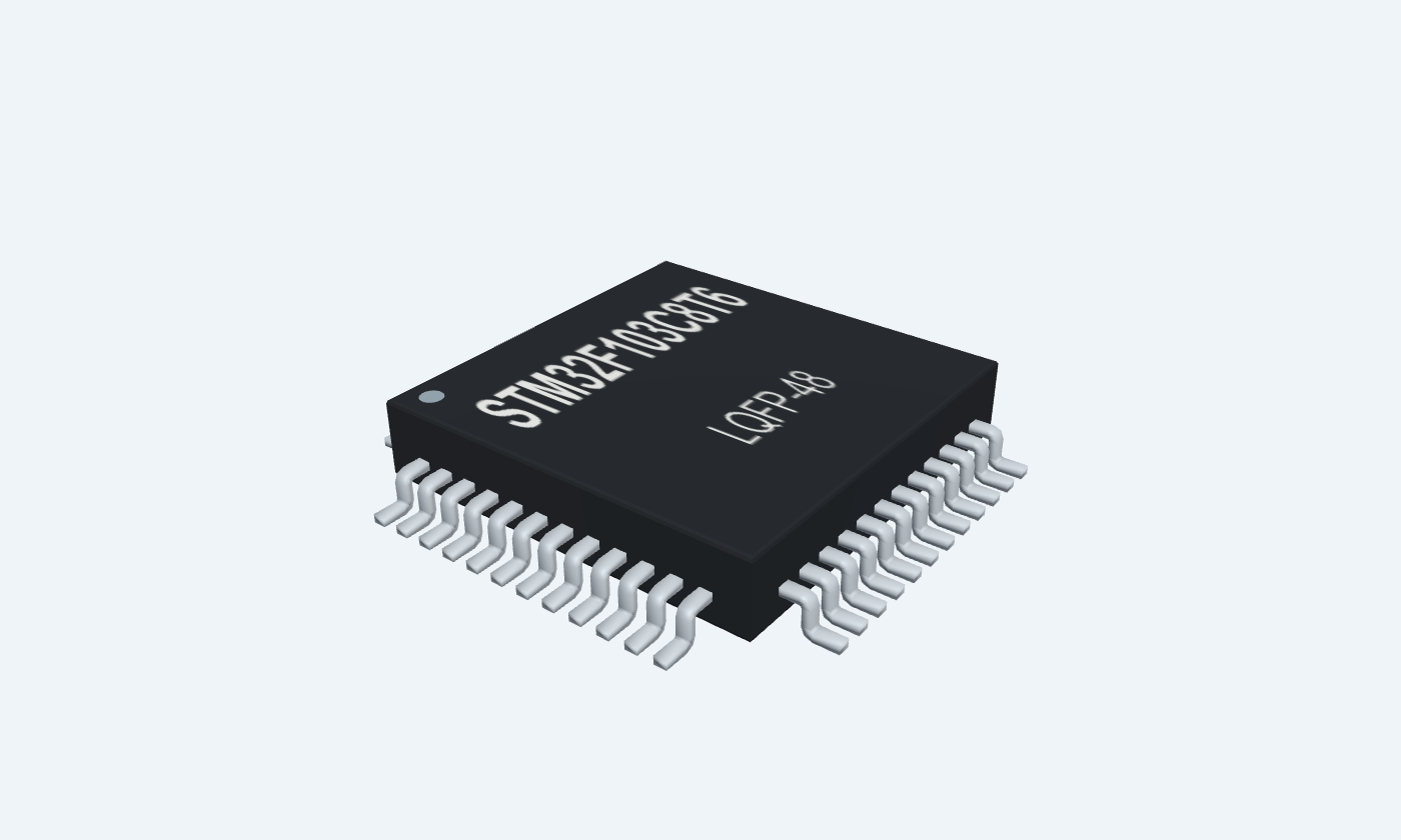
A 72 MHz controller with a compact, versatile peripheral set.
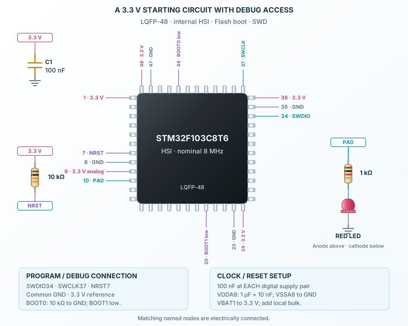
STM32F103C8T6 is a 32-bit Arm Cortex-M3 microcontroller in a 48-lead LQFP package. The C8 device has 64 KB of specified Flash and 20 KB of SRAM, with timers, DMA, serial interfaces and two twelve-bit ADCs. Its maximum system frequency is 72 MHz with a correctly configured clock tree. The part operates from 2.0 to 3.6 V, with additional analog supply conditions when using the ADC. Every digital supply pair, the analog rail and the backup input need deliberate connections. Some digital pins tolerate 5 V under specified conditions, but this does not apply to every pin or to analog inputs. The reference circuit uses 3.3 V and the reset-default 8 MHz internal oscillator, so its simple LED demonstration needs no external crystal. SWD remains accessible, BOOT0 is held low and firmware starts from Flash. Higher-speed, USB and precision-timing applications need their own reviewed clock configuration.
Click a lead or use the arrow keys. Top view
Supply connection for the named power domain.
Connect to 3.3 V when no separate backup battery is fitted.
Connect every supply domain; do not leave VDDA or VBAT floating.
Multiplexed GPIO and the named default alternate function; remapping and peripheral configuration may change its use.
Connect only to compatible signal levels and configure the pin mode.
PC13–PC15 have restricted drive: do not use as LED current sources; observe 3 mA switch and speed limits.
GPIO multiplexed with the selected crystal oscillator function.
Leave oscillator pins unused when running only from HSI; add correctly loaded crystals when selected.
PC13–PC15 have restricted drive: do not use as LED current sources; observe 3 mA switch and speed limits.
GPIO multiplexed with the selected crystal oscillator function.
Leave oscillator pins unused when running only from HSI; add correctly loaded crystals when selected.
PC13–PC15 have restricted drive: do not use as LED current sources; observe 3 mA switch and speed limits.
GPIO multiplexed with the selected crystal oscillator function.
Leave oscillator pins unused when running only from HSI; add correctly loaded crystals when selected.
Check the datasheet pin type before applying 5 V; tolerance depends on pin and operating mode.
GPIO multiplexed with the selected crystal oscillator function.
Leave oscillator pins unused when running only from HSI; add correctly loaded crystals when selected.
Check the datasheet pin type before applying 5 V; tolerance depends on pin and operating mode.
Active-low device reset.
Expose to the SWD header; optional reset button to ground.
Check the datasheet pin type before applying 5 V; tolerance depends on pin and operating mode.
Supply connection for the named power domain.
Connect to common ground.
Connect every supply domain; do not leave VDDA or VBAT floating.
Supply connection for the named power domain.
Connect to 3.3 V with local 1 µF and 10 nF analog bypass.
Connect every supply domain; do not leave VDDA or VBAT floating.
Multiplexed GPIO and the named default alternate function; remapping and peripheral configuration may change its use.
Example LED output through 1 kΩ to ground.
ADC input channel 0; not a 5 V-tolerant analog input. Keep analog voltage within VSSA–VDDA.
Multiplexed GPIO and the named default alternate function; remapping and peripheral configuration may change its use.
Connect only to compatible signal levels and configure the pin mode.
ADC input channel 1; not a 5 V-tolerant analog input. Keep analog voltage within VSSA–VDDA.
Multiplexed GPIO and the named default alternate function; remapping and peripheral configuration may change its use.
Connect only to compatible signal levels and configure the pin mode.
ADC input channel 2; not a 5 V-tolerant analog input. Keep analog voltage within VSSA–VDDA.
Multiplexed GPIO and the named default alternate function; remapping and peripheral configuration may change its use.
Connect only to compatible signal levels and configure the pin mode.
ADC input channel 3; not a 5 V-tolerant analog input. Keep analog voltage within VSSA–VDDA.
Multiplexed GPIO and the named default alternate function; remapping and peripheral configuration may change its use.
Connect only to compatible signal levels and configure the pin mode.
ADC input channel 4; not a 5 V-tolerant analog input. Keep analog voltage within VSSA–VDDA.
Multiplexed GPIO and the named default alternate function; remapping and peripheral configuration may change its use.
Connect only to compatible signal levels and configure the pin mode.
ADC input channel 5; not a 5 V-tolerant analog input. Keep analog voltage within VSSA–VDDA.
Multiplexed GPIO and the named default alternate function; remapping and peripheral configuration may change its use.
Connect only to compatible signal levels and configure the pin mode.
ADC input channel 6; not a 5 V-tolerant analog input. Keep analog voltage within VSSA–VDDA.
Multiplexed GPIO and the named default alternate function; remapping and peripheral configuration may change its use.
Connect only to compatible signal levels and configure the pin mode.
ADC input channel 7; not a 5 V-tolerant analog input. Keep analog voltage within VSSA–VDDA.
Multiplexed GPIO and the named default alternate function; remapping and peripheral configuration may change its use.
Connect only to compatible signal levels and configure the pin mode.
ADC input channel 8; not a 5 V-tolerant analog input. Keep analog voltage within VSSA–VDDA.
Multiplexed GPIO and the named default alternate function; remapping and peripheral configuration may change its use.
Connect only to compatible signal levels and configure the pin mode.
ADC input channel 9; not a 5 V-tolerant analog input. Keep analog voltage within VSSA–VDDA.
Multiplexed GPIO and the named default alternate function; remapping and peripheral configuration may change its use.
Define BOOT1 level; use low for the reference circuit.
Check the datasheet pin type before applying 5 V; tolerance depends on pin and operating mode.
Multiplexed GPIO and the named default alternate function; remapping and peripheral configuration may change its use.
Connect only to compatible signal levels and configure the pin mode.
Check the datasheet pin type before applying 5 V; tolerance depends on pin and operating mode.
Multiplexed GPIO and the named default alternate function; remapping and peripheral configuration may change its use.
Connect only to compatible signal levels and configure the pin mode.
Check the datasheet pin type before applying 5 V; tolerance depends on pin and operating mode.
Supply connection for the named power domain.
Connect to common ground.
Connect every supply domain; do not leave VDDA or VBAT floating.
Supply connection for the named power domain.
Connect to 3.3 V and bypass locally with 100 nF.
Connect every supply domain; do not leave VDDA or VBAT floating.
Multiplexed GPIO and the named default alternate function; remapping and peripheral configuration may change its use.
Connect only to compatible signal levels and configure the pin mode.
Check the datasheet pin type before applying 5 V; tolerance depends on pin and operating mode.
Multiplexed GPIO and the named default alternate function; remapping and peripheral configuration may change its use.
Connect only to compatible signal levels and configure the pin mode.
Check the datasheet pin type before applying 5 V; tolerance depends on pin and operating mode.
Multiplexed GPIO and the named default alternate function; remapping and peripheral configuration may change its use.
Connect only to compatible signal levels and configure the pin mode.
Check the datasheet pin type before applying 5 V; tolerance depends on pin and operating mode.
Multiplexed GPIO and the named default alternate function; remapping and peripheral configuration may change its use.
Connect only to compatible signal levels and configure the pin mode.
Check the datasheet pin type before applying 5 V; tolerance depends on pin and operating mode.
Multiplexed GPIO and the named default alternate function; remapping and peripheral configuration may change its use.
Connect only to compatible signal levels and configure the pin mode.
Check the datasheet pin type before applying 5 V; tolerance depends on pin and operating mode.
Multiplexed GPIO and the named default alternate function; remapping and peripheral configuration may change its use.
Connect only to compatible signal levels and configure the pin mode.
Check the datasheet pin type before applying 5 V; tolerance depends on pin and operating mode.
Multiplexed GPIO and the named default alternate function; remapping and peripheral configuration may change its use.
Connect only to compatible signal levels and configure the pin mode.
Check the datasheet pin type before applying 5 V; tolerance depends on pin and operating mode.
Multiplexed GPIO and the named default alternate function; remapping and peripheral configuration may change its use.
Connect only to compatible signal levels and configure the pin mode.
USB data pins are not general 5 V-tolerant inputs. USB needs its specified clock and external interface network.
Multiplexed GPIO and the named default alternate function; remapping and peripheral configuration may change its use.
Connect only to compatible signal levels and configure the pin mode.
USB data pins are not general 5 V-tolerant inputs. USB needs its specified clock and external interface network.
Debug port function at reset; some pins can be released to GPIO with software configuration.
Connect to a 3.3 V-compatible SWD programmer.
Check the datasheet pin type before applying 5 V; tolerance depends on pin and operating mode.
Supply connection for the named power domain.
Connect to common ground.
Connect every supply domain; do not leave VDDA or VBAT floating.
Supply connection for the named power domain.
Connect to 3.3 V and bypass locally with 100 nF.
Connect every supply domain; do not leave VDDA or VBAT floating.
Debug port function at reset; some pins can be released to GPIO with software configuration.
Connect to a 3.3 V-compatible SWD programmer.
Check the datasheet pin type before applying 5 V; tolerance depends on pin and operating mode.
Debug port function at reset; some pins can be released to GPIO with software configuration.
Connect only to compatible signal levels and configure the pin mode.
Check the datasheet pin type before applying 5 V; tolerance depends on pin and operating mode.
Debug port function at reset; some pins can be released to GPIO with software configuration.
Connect only to compatible signal levels and configure the pin mode.
Check the datasheet pin type before applying 5 V; tolerance depends on pin and operating mode.
Debug port function at reset; some pins can be released to GPIO with software configuration.
Connect only to compatible signal levels and configure the pin mode.
Check the datasheet pin type before applying 5 V; tolerance depends on pin and operating mode.
Multiplexed GPIO and the named default alternate function; remapping and peripheral configuration may change its use.
Connect only to compatible signal levels and configure the pin mode.
Check the datasheet pin type before applying 5 V; tolerance depends on pin and operating mode.
Multiplexed GPIO and the named default alternate function; remapping and peripheral configuration may change its use.
Connect only to compatible signal levels and configure the pin mode.
Check the datasheet pin type before applying 5 V; tolerance depends on pin and operating mode.
Multiplexed GPIO and the named default alternate function; remapping and peripheral configuration may change its use.
Connect only to compatible signal levels and configure the pin mode.
Check the datasheet pin type before applying 5 V; tolerance depends on pin and operating mode.
Boot-mode selection sampled at reset.
10 kΩ pull-down to ground for normal Flash boot.
Check the datasheet pin type before applying 5 V; tolerance depends on pin and operating mode.
Multiplexed GPIO and the named default alternate function; remapping and peripheral configuration may change its use.
Connect only to compatible signal levels and configure the pin mode.
Check the datasheet pin type before applying 5 V; tolerance depends on pin and operating mode.
Multiplexed GPIO and the named default alternate function; remapping and peripheral configuration may change its use.
Connect only to compatible signal levels and configure the pin mode.
Check the datasheet pin type before applying 5 V; tolerance depends on pin and operating mode.
Supply connection for the named power domain.
Connect to common ground.
Connect every supply domain; do not leave VDDA or VBAT floating.
Supply connection for the named power domain.
Connect to 3.3 V and bypass locally with 100 nF.
Connect every supply domain; do not leave VDDA or VBAT floating.
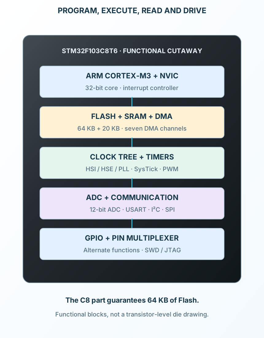
32-bit Arm Cortex-M3 microcontroller
The Cortex-M3 core and DMA share memory and peripheral buses; GPIO selects which functions reach the pins.
STM32F103C8T6
Key parameters and their test conditions
Follows the selected physical package
Select a pin to open its function, electrical notes and wiring guidance.
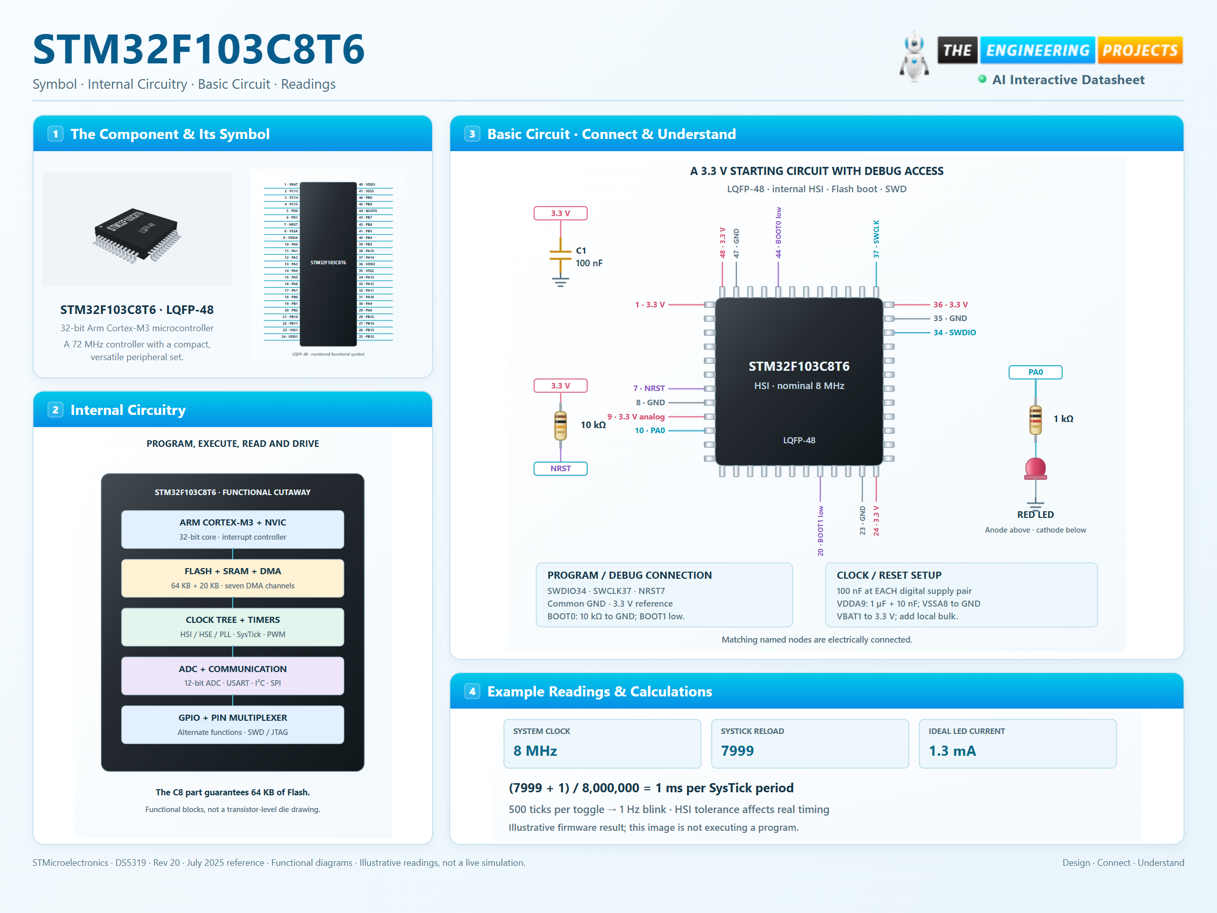
Connect VDD, VDDA, VBAT and all returns with local bypass.
Use SWDIO, SWCLK, reset, ground and a 3.3 V reference.
Configure buses, Flash latency and GPIO deliberately before increasing speed.
At HCLK = 8 MHz, SysTick clocked from HCLK with LOAD = 7999 gives a nominal 1 ms tick. Count 500 ticks for each LED toggle.
Select a pin to explore its function and connection.
| Pin | Signal | Type | Function |
|---|---|---|---|
| VBAT | Supply | Supply connection for the named power domain. | |
| PC13 / TAMPER | Multiplexed pin | Multiplexed GPIO and the named default alternate function; remapping and peripheral configuration may change its use. | |
| PC14 / OSC32_IN | Multiplexed pin | GPIO multiplexed with the selected crystal oscillator function. | |
| PC15 / OSC32_OUT | Multiplexed pin | GPIO multiplexed with the selected crystal oscillator function. | |
| PD0 / OSC_IN | Multiplexed pin | GPIO multiplexed with the selected crystal oscillator function. | |
| PD1 / OSC_OUT | Multiplexed pin | GPIO multiplexed with the selected crystal oscillator function. | |
| NRST | Multiplexed pin | Active-low device reset. | |
| VSSA | Supply | Supply connection for the named power domain. | |
| VDDA | Supply | Supply connection for the named power domain. | |
| PA0 / WKUP | Multiplexed pin | Multiplexed GPIO and the named default alternate function; remapping and peripheral configuration may change its use. | |
| PA1 | Multiplexed pin | Multiplexed GPIO and the named default alternate function; remapping and peripheral configuration may change its use. | |
| PA2 / USART2_TX | Multiplexed pin | Multiplexed GPIO and the named default alternate function; remapping and peripheral configuration may change its use. | |
| PA3 / USART2_RX | Multiplexed pin | Multiplexed GPIO and the named default alternate function; remapping and peripheral configuration may change its use. | |
| PA4 / SPI1_NSS | Multiplexed pin | Multiplexed GPIO and the named default alternate function; remapping and peripheral configuration may change its use. | |
| PA5 / SPI1_SCK | Multiplexed pin | Multiplexed GPIO and the named default alternate function; remapping and peripheral configuration may change its use. | |
| PA6 / SPI1_MISO | Multiplexed pin | Multiplexed GPIO and the named default alternate function; remapping and peripheral configuration may change its use. | |
| PA7 / SPI1_MOSI | Multiplexed pin | Multiplexed GPIO and the named default alternate function; remapping and peripheral configuration may change its use. | |
| PB0 | Multiplexed pin | Multiplexed GPIO and the named default alternate function; remapping and peripheral configuration may change its use. | |
| PB1 | Multiplexed pin | Multiplexed GPIO and the named default alternate function; remapping and peripheral configuration may change its use. | |
| PB2 / BOOT1 | Multiplexed pin | Multiplexed GPIO and the named default alternate function; remapping and peripheral configuration may change its use. | |
| PB10 / I2C2_SCL | Multiplexed pin | Multiplexed GPIO and the named default alternate function; remapping and peripheral configuration may change its use. | |
| PB11 / I2C2_SDA | Multiplexed pin | Multiplexed GPIO and the named default alternate function; remapping and peripheral configuration may change its use. | |
| VSS1 | Supply | Supply connection for the named power domain. | |
| VDD1 | Supply | Supply connection for the named power domain. | |
| PB12 / SPI2_NSS | Multiplexed pin | Multiplexed GPIO and the named default alternate function; remapping and peripheral configuration may change its use. | |
| PB13 / SPI2_SCK | Multiplexed pin | Multiplexed GPIO and the named default alternate function; remapping and peripheral configuration may change its use. | |
| PB14 / SPI2_MISO | Multiplexed pin | Multiplexed GPIO and the named default alternate function; remapping and peripheral configuration may change its use. | |
| PB15 / SPI2_MOSI | Multiplexed pin | Multiplexed GPIO and the named default alternate function; remapping and peripheral configuration may change its use. | |
| PA8 / MCO | Multiplexed pin | Multiplexed GPIO and the named default alternate function; remapping and peripheral configuration may change its use. | |
| PA9 / USART1_TX | Multiplexed pin | Multiplexed GPIO and the named default alternate function; remapping and peripheral configuration may change its use. | |
| PA10 / USART1_RX | Multiplexed pin | Multiplexed GPIO and the named default alternate function; remapping and peripheral configuration may change its use. | |
| PA11 / USB_DM | Multiplexed pin | Multiplexed GPIO and the named default alternate function; remapping and peripheral configuration may change its use. | |
| PA12 / USB_DP | Multiplexed pin | Multiplexed GPIO and the named default alternate function; remapping and peripheral configuration may change its use. | |
| PA13 / SWDIO | Debug / GPIO | Debug port function at reset; some pins can be released to GPIO with software configuration. | |
| VSS2 | Supply | Supply connection for the named power domain. | |
| VDD2 | Supply | Supply connection for the named power domain. | |
| PA14 / SWCLK | Debug / GPIO | Debug port function at reset; some pins can be released to GPIO with software configuration. | |
| PA15 / JTDI | Debug / GPIO | Debug port function at reset; some pins can be released to GPIO with software configuration. | |
| PB3 / JTDO | Debug / GPIO | Debug port function at reset; some pins can be released to GPIO with software configuration. | |
| PB4 / NJTRST | Debug / GPIO | Debug port function at reset; some pins can be released to GPIO with software configuration. | |
| PB5 | Multiplexed pin | Multiplexed GPIO and the named default alternate function; remapping and peripheral configuration may change its use. | |
| PB6 / I2C1_SCL | Multiplexed pin | Multiplexed GPIO and the named default alternate function; remapping and peripheral configuration may change its use. | |
| PB7 / I2C1_SDA | Multiplexed pin | Multiplexed GPIO and the named default alternate function; remapping and peripheral configuration may change its use. | |
| BOOT0 | Multiplexed pin | Boot-mode selection sampled at reset. | |
| PB8 | Multiplexed pin | Multiplexed GPIO and the named default alternate function; remapping and peripheral configuration may change its use. | |
| PB9 | Multiplexed pin | Multiplexed GPIO and the named default alternate function; remapping and peripheral configuration may change its use. | |
| VSS3 | Supply | Supply connection for the named power domain. | |
| VDD3 | Supply | Supply connection for the named power domain. |
No pins match. Try a signal name or choose All pins.
Do not substitute larger family members
| Parameter | Value | Conditions / notes |
|---|---|---|
| Core | Arm Cortex-M3 | 32-bit; no hardware floating-point unit |
| Maximum SYSCLK | 72 MHz | Requires valid clock and Flash settings |
| Flash | 64 KB | C8 guarantee; do not rely on undocumented extra memory |
| SRAM | 20 KB | Application data and stack |
| Package | 48-lead LQFP, 7 × 7 mm | 0.5 mm lead pitch |
| Temperature suffix 6 | −40 to +85°C | Selected C8T6 |
| GPIO | Up to 37 I/O | Some consumed by clocks, debug or peripherals |
No specifications match. Try a parameter name or a unit.
The device name describes memory, pin count, package and temperature grade.
3.3 V reference circuit
| Parameter | Value | Conditions / notes |
|---|---|---|
| VDD1 / VDD2 / VDD3 | Pins 24 / 36 / 48 | 3.3 V; 100 nF near each pair plus local bulk |
| VSS1 / VSS2 / VSS3 | Pins 23 / 35 / 47 | Common ground |
| VDDA / VSSA | Pins 9 / 8 | Analog rail and return; 1 µF + 10 nF bypass |
| VBAT | Pin 1 | Tie to VDD when no separate backup supply is used |
| Digital VDD | 2.0–3.6 V | Recommended range |
| ADC VDDA | 2.4–3.6 V | Specified ADC operating range |
| Input tolerance | Pin and mode dependent | Do not feed 5 V into an analog input |
No specifications match. Try a parameter name or a unit.
All supply contacts are required even for a minimal program.
Firmware controls the operating speed
| Parameter | Value | Conditions / notes |
|---|---|---|
| Reset system clock | Internal HSI, nominal 8 MHz | Used by this example |
| External HSE crystal | 4–16 MHz | Select load capacitors for the crystal |
| HSI PLL input | HSI divided by 2 | PLL multiplier limits still apply |
| SYSCLK / AHB | Up to 72 MHz | Match Flash latency and supply conditions |
| APB1 | Up to 36 MHz | Use a divider at 72 MHz SYSCLK |
| APB2 | Up to 72 MHz | Independent peripheral enables |
| ADC clock | Up to 14 MHz | Select ADC prescaler and sampling time |
| USB clock | 48 MHz with specified accuracy | Reset HSI-only example is not a USB design |
No specifications match. Try a parameter name or a unit.
A 72 MHz target constant does not configure the hardware clock tree.
Keep a recoverable SWD path
| Parameter | Value | Conditions / notes |
|---|---|---|
| Normal Flash boot | BOOT0 low | 10 kΩ pull-down on pin 44 |
| System memory | BOOT0 high, BOOT1 low | Built-in serial bootloader; check ST bootloader documentation |
| SRAM boot | BOOT0 high, BOOT1 high | Special development use |
| BOOT1 | PB2 pin 20 | Defined low in the reference |
| SWDIO / SWCLK | PA13 pin 34 / PA14 pin 37 | 3.3 V-compatible programmer |
| NRST | Pin 7 | Expose reset to programmer; optional button |
| JTAG pins | PA15 / PB3 / PB4 also reserved initially | Disable JTAG while retaining SWD if these GPIO are needed |
No specifications match. Try a parameter name or a unit.
Do not enable readout protection or remove debug access casually.
Default mappings; selected remaps exist
| Parameter | Value | Conditions / notes |
|---|---|---|
| USART1 TX / RX | PA9-30 / PA10-31 | Logic levels, not RS-232 voltage |
| USART2 TX / RX | PA2-12 / PA3-13 | Shared with ADC inputs |
| I²C1 SCL / SDA | PB6-42 / PB7-43 | External pull-ups to a compatible rail |
| I²C2 SCL / SDA | PB10-21 / PB11-22 | Open-drain bus configuration |
| SPI1 NSS / SCK / MISO / MOSI | PA4-14 / PA5-15 / PA6-16 / PA7-17 | Shared analog-capable pins |
| SPI2 NSS / SCK / MISO / MOSI | PB12-25 / PB13-26 / PB14-27 / PB15-28 | Configure chip select deliberately |
| USB DM / DP | PA11-32 / PA12-33 | External interface and accurate clock required |
| CAN | Shared resources with USB | External CAN transceiver required |
No specifications match. Try a parameter name or a unit.
The peripheral block does not supply external bus transceivers or pull-ups.
48-pin device details
| Parameter | Value | Conditions / notes |
|---|---|---|
| External ADC channels | PA0–PA7 and PB0–PB1 | Ten externally available inputs |
| ADC resolution | 12-bit | Sampling time and source impedance affect accuracy |
| Reference | VDDA / VSSA on this package | No separate external VREF pins |
| Calibration | Run after power-up | Follow ADC initialization sequence |
| PC13–PC15 | Restricted output drive | Do not source LED current from these pins |
| LED example | PA0 pin 10 | General push-pull output in this circuit |
| Analog input span | VSSA through VDDA | No 5 V tolerance in analog mode |
No specifications match. Try a parameter name or a unit.
The internal temperature sensor measures die temperature, not a guaranteed ambient temperature.
No external oscillator required
| Parameter | Value | Conditions / notes |
|---|---|---|
| Supply | 3.3 V to all required rails | Local decoupling and a bulk capacitor |
| BOOT0 / BOOT1 | Defined low | Boot from programmed Flash |
| Output | PA0-10 → 1 kΩ → red LED → GND | Ideal current about 1.3 mA for a 2 V LED |
| GPIO setup | Enable GPIOA clock; set PA0 output | Choose low output speed and known initial state |
| SysTick clock | HCLK = 8 MHz | Select core clock as SysTick source |
| SysTick reload | 7999 | (7999 + 1) / 8 MHz = 1 ms |
| Blink | Toggle every 500 ticks | Nominal full cycle 1 second |
No specifications match. Try a parameter name or a unit.
Actual RC oscillator tolerance affects timing; the illustration is not firmware execution.
Timers, interrupts and serial links.
Manufacturer application guideADC with DMA and deliberate sampling.
Manufacturer application guideAdd the required external interface hardware.
Manufacturer application guideFind STM32F103C8T6 in the Components Library to place its schematic symbol and connect its pins.
Reference page · circuit simulation model not yet availableOpen ProTech