Hello friends! In this tutorial, we will design an LED blinking project using the PIC16F877A microcontroller. It is a simple project, but it introduces several ideas that appear in almost every embedded system: configuring an I/O port, choosing an oscillator, building a reset circuit, calculating LED resistors, generating a time delay, compiling a program, and loading the resulting HEX file into Proteus.
We will connect eight LEDs to PORTB and switch the complete port between logic low and logic high. Once this basic version works, you can change the output patterns and timing to create a running light, binary counter, or status display. The important objective is to understand why every connection and every program statement is present.
PIC16F877A Overview
The PIC16F877A is an 8-bit microcontroller from Microchip's PIC16F87XA family. It has a 14-bit instruction word, Flash program memory, RAM, data EEPROM, timers, an analog-to-digital converter, two Capture/Compare/PWM modules, a USART, and serial interfaces that can operate as SPI or I²C. For this first project, we only need its clock, reset, power, and PORTB digital-output functions.
The 40-pin PDIP device provides eight PORTB pins named RB0 through RB7. The TRISB register controls their direction. A TRIS bit equal to 1 makes its corresponding pin an input; a bit equal to 0 makes it an output. Therefore, writing TRISB = 0x00 configures all eight PORTB pins as outputs.
| Resource | Purpose in the circuit |
|---|---|
| VDD and VSS pins | Provide power and ground to the microcontroller |
| MCLR/VPP | Provides an active-low hardware reset and programming voltage input |
| OSC1 and OSC2 | Connect the external crystal or resonator |
| RB0 through RB7 | Drive the eight LEDs |
| TRISB | Selects whether each PORTB pin is an input or output |
| PORTB | Writes the output pattern presented at the pins |
Microchip lists the PIC16F877A as an in-production device and provides the complete electrical limits and pin descriptions in the PIC16F877A product documentation. Always use the datasheet for the package and device revision in your actual design.
Project Objective and Blinking Sequence
All eight LEDs will turn on for two seconds and then turn off for two seconds. The sequence repeats continuously:
- Configure PORTB as a digital output port.
- Write
0xFFto make RB7 through RB0 high. - Wait for two seconds.
- Write
0x00to make RB7 through RB0 low. - Wait for another two seconds and repeat.
This assumes each LED is connected from a PORTB output through its own series resistor to ground, so a high output turns it on. If an LED is connected from VDD through a resistor to the pin, it becomes active low: the pin must sink current and a low output turns it on. State the chosen arrangement before interpreting the output values.
Components Required
| Component | Quantity | Selection note |
|---|---|---|
| PIC16F877A | 1 | Use the correct 40-pin device in Proteus |
| LED | 8 | One LED for every PORTB bit |
| LED series resistor | 8 | Calculate one resistor for each LED branch |
| 16 MHz crystal | 1 | Used with HS oscillator configuration |
| Crystal load capacitor | 2 | Select using crystal and Microchip guidance |
| MCLR pull-up resistor | 1 | 10 kΩ is a common starting value |
| 100 nF ceramic bypass capacitor | At least 2 | Place close to the VDD/VSS pin pairs on hardware |
| Regulated 5 V supply | 1 | Observe the device and total load requirements |
| Programmer/debugger | 1 | Required for a physical microcontroller |
The original tutorial used Proteus and the mikroC PRO for PIC compiler. We will preserve that path first because it matches the downloadable project and screenshots. An MPLAB X and XC8 alternative is included later for readers using Microchip's current toolchain.
Calculate the LED Resistors
Every LED needs its own series resistor. One resistor shared by several parallel LEDs does not control the current of each branch reliably because LED forward voltages are not identical.
For an LED connected from an output pin to ground, estimate the resistor using Ohm's law:
R = (VOH - VF) / ILED
Assume a 5 V supply, an illustrative red LED forward voltage of 2.0 V, and a target current of 5 mA. Using 5 V as a simple upper estimate gives:
R = (5.0 - 2.0) / 0.005 = 600 Ω
The next common value, 680 Ω, gives an approximate current of:
I = (5.0 - 2.0) / 680 = 4.41 mA
The actual current depends on the LED, resistor tolerance, supply voltage, and the microcontroller's loaded output voltage. Use the datasheet's guaranteed output characteristics rather than assuming an output remains exactly at VDD under load.
If eight branches each draw approximately 4.41 mA, the PORTB LED load is about:
IPORTB = 8 × 4.41 = 35.28 mA
Check both the per-pin and combined-port limits. An absolute maximum is a damage boundary, not a recommended operating target. The PIC16F87XA datasheet lists the applicable limits and DC output characteristics.
For a physical build, a lower LED current reduces load and heat. If you require brighter or higher-current LEDs, use suitable transistor or driver outputs rather than increasing pin current toward the absolute maximum.
Build the PIC16F877A Basic Circuit
Download the original Proteus simulation and project files if you want to compare them with your own circuit. Designing the circuit yourself first is the better learning exercise.
Download the Proteus simulation and code
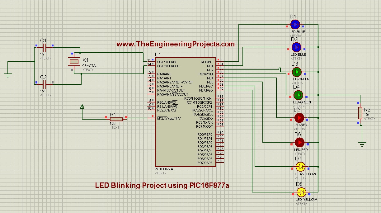
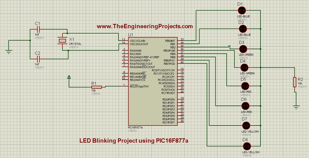
The complete Proteus circuit is shown in the original project image:
Connect Power Correctly
The 40-pin PIC16F877A has two VDD pins and two VSS pins. Connect every VDD to the regulated positive supply and every VSS to ground. On a real board, place a 100 nF ceramic bypass capacitor close to each VDD/VSS pair. The short connection helps the capacitor supply rapid current changes locally.
A 12 V adapter must not be connected directly to VDD. If you use a linear regulator such as a 7805, calculate its heat dissipation. For an illustrative total load of 60 mA:
P = (Vin - Vout) × I = (12 - 5) × 0.060 = 0.42 W
That heat is produced in the regulator. Input and output capacitors, regulator package, airflow, input tolerance, and reverse-current conditions also matter. A regulated bench supply or a suitably designed 5 V supply is more convenient for a first hardware test.
Connect MCLR
MCLR is an active-low reset input. Pull it up to VDD through a resistor so that noise does not leave the pin floating. A pushbutton can pull MCLR to ground for manual reset if the circuit includes the recommended reset arrangement.
Do not place a large capacitor on MCLR without checking the programming/debugger requirements. The same pin receives the programming voltage, and the programming tool must be able to control it correctly.
Connect the 16 MHz Crystal
Place the crystal between OSC1 and OSC2. Connect a load capacitor from each crystal terminal to ground, keeping the traces short and clear of noisy output signals on a physical PCB. Select HS oscillator mode for this 16 MHz crystal arrangement.
Do not choose the capacitors using frequency alone. A crystal specifies a load capacitance, and the circuit also has pin and PCB stray capacitance. For approximately equal capacitors:
CL ≈ C / 2 + Cstray
If a crystal specifies 18 pF load capacitance and you estimate 4 pF stray capacitance, the illustrative result is:
C ≈ 2 × (18 - 4) = 28 pF
A standard value near that result may be evaluated, but the crystal manufacturer's recommendation and Microchip oscillator guidance take priority. The old statement that changing frequency automatically requires one fixed capacitor value is too broad.
Connect PORTB LEDs
Connect RB0 through RB7 to separate LED-and-resistor branches. For the active-high arrangement, connect each output to a resistor, then the LED anode, and connect the cathode to ground. You may reverse the order of the series resistor and LED without changing the branch current.
Check LED polarity before debugging the program. In Proteus, the component symbol shows anode and cathode. On common through-hole LEDs, the shorter lead and flat package edge often identify the cathode, but confirm the component documentation rather than relying on appearance alone.
Understand the Clock and Delay
The PIC16F877A instruction-cycle period is:
TCY = 4 / FOSC
At a 16 MHz oscillator frequency:
TCY = 4 / 16,000,000 = 0.25 µs
The instruction clock is therefore 4 MHz. A two-second delay represents about:
2 s / 0.25 µs = 8,000,000 instruction cycles
A compiler delay routine creates the required loops and instruction sequence for the selected clock. If the project tells the compiler that the clock is 16 MHz while the simulation or hardware runs at another frequency, the visible delay will be wrong by the same ratio.
With two seconds on and two seconds off, one complete blinking period is four seconds:
T = 2 + 2 = 4 s
The blinking frequency and duty cycle are:
f = 1 / T = 1 / 4 = 0.25 Hz
Duty cycle = Ton / T × 100 = 2 / 4 × 100 = 50%
Program the Project with mikroC PRO for PIC
Create a new mikroC PRO for PIC project, select PIC16F877A, and set the oscillator frequency to 16 MHz. Set the configuration so that it matches the external high-speed crystal and your hardware choices. Then use this code:
void main() {
    TRISB = 0x00;
    PORTB = 0x00;

    while (1) {
        PORTB = 0xFF;
        Delay_ms(2000);

        PORTB = 0x00;
        Delay_ms(2000);
    }
}
TRISB = 0x00 writes eight zero bits to the data-direction register. Every PORTB pin therefore becomes an output. Initializing PORTB before the loop establishes a known off state instead of relying on assumptions about startup.
PORTB = 0xFF writes binary 11111111, so all eight output bits become high. In the active-high circuit, all LEDs turn on. PORTB = 0x00 writes binary 00000000, switching them off.
The infinite while (1) loop keeps the sequence running for as long as the microcontroller remains powered and out of reset. The delay function blocks the processor during each wait. Blocking is acceptable for this one-purpose demonstration, but a timer-based design is preferable when the controller must perform other work while the LED timing continues.
Alternative MPLAB X and XC8 Code
If you are using MPLAB X IDE with the XC8 compiler, create a standalone project for PIC16F877A. Generate configuration directives through the IDE's Configuration Bits window, review each setting against the datasheet, and add the generated directives to the source file. A representative main program is:
#include <xc.h>

#define _XTAL_FREQ 16000000UL

// Add the configuration-bit directives generated for your project here.

void main(void) {
    TRISB = 0x00;
    PORTB = 0x00;

    while (1) {
        PORTB = 0xFF;
        __delay_ms(2000);

        PORTB = 0x00;
        __delay_ms(2000);
    }
}
The _XTAL_FREQ macro tells XC8 the system clock used when calculating its delay sequence; it does not configure the oscillator hardware. Microchip's XC8 compiler guide requires that value to match the real device clock for __delay_ms() and __delay_us().
Configuration bits control the clock source, watchdog timer, brown-out behavior, low-voltage programming, code protection, and other startup behavior. Copying an unexplained group of directives can produce a HEX file that compiles yet behaves differently from the circuit. Use MPLAB X to generate the directives, then document the choices.
Build the HEX File and Run the Proteus Simulation
- Build the compiler project and confirm that it finishes without errors.
- Locate the generated HEX file in the compiler's output folder.
- Open the PIC16F877A properties in Proteus.
- Select the generated HEX file as the program file.
- Set the component clock frequency to 16 MHz so it matches the project.
- Start the simulation and observe the PORTB LEDs.
The expected result is shown in the original simulation image:
Proteus can demonstrate the program sequence and basic circuit behavior, but it does not replace checking real supply quality, crystal startup, programmer connections, output voltage under load, or component tolerances. Treat the simulation as one step in the engineering process.
Create Other LED Patterns
A byte written to PORTB maps directly to the eight output bits. This makes PORTB a convenient visual introduction to binary values.
| Hexadecimal | Binary | Active-high result |
|---|---|---|
0x00 | 00000000 | All LEDs off |
0x01 | 00000001 | RB0 LED on |
0x0F | 00001111 | Lower four LEDs on |
0x55 | 01010101 | Alternating LEDs on |
0xAA | 10101010 | The opposite alternating LEDs on |
0xFF | 11111111 | All LEDs on |
For a running LED, start with 0x01 and shift the bit left after each delay. Remember that C integer promotion and the behavior after shifting beyond RB7 need to be handled explicitly. A byte variable can be reset to 0x01 after it becomes zero.
Troubleshooting the Project
| Symptom | Likely cause | First check |
|---|---|---|
| No LEDs operate | Missing power, reset held low, oscillator problem, or HEX not loaded | Check all VDD/VSS pins, MCLR, clock, and program path |
| LEDs remain continuously on | Program stopped, wrong delay expectation, or reset/clock issue | Confirm that PORTB changes in simulation and the clock is 16 MHz |
| Only some LEDs work | LED polarity, missing resistor branch, wiring, or damaged output | Inspect each RB pin-to-LED path separately |
| Blink timing is incorrect | Compiler and circuit clock settings differ | Compare project oscillator value, configuration bits, crystal, and Proteus clock |
| RB3 behaves unexpectedly | Low-voltage programming remains enabled | Review the LVP configuration and programming method |
| Physical circuit resets as LEDs switch | Supply drop or inadequate decoupling | Measure VDD at the PIC and inspect bypass capacitors |
Change one item at a time. If you replace the HEX file, oscillator settings, resistor values, and wiring simultaneously, a successful result will not tell you which change corrected the problem.
Practical Review
This project teaches more than blinking LEDs. TRISB establishes direction, PORTB defines the output pattern, and the oscillator determines instruction timing. The external circuit then converts the port voltage into visible light while resistors control current.
The calculation section is part of the design, not an optional addition. Each LED needs its own resistor, the combined load must remain within the device limits, the regulator must dissipate its heat safely, and the compiler's clock definition must agree with the actual oscillator.
Once this version works, replace the blocking delays with a hardware timer and let the main loop perform another task. That change turns a demonstration into the foundation of a responsive embedded application.
Frequently Asked Questions
Why does a zero in TRISB make a pin an output?
For this PIC family, a TRIS bit of 1 places the output driver in a high-impedance input state, while 0 enables output operation. A common memory aid is that 1 resembles the letter I for input.
Do I need eight resistors for eight LEDs?
Yes. Use one correctly calculated series resistor in each LED branch. Sharing one resistor among parallel LEDs does not ensure equal or controlled branch current.
Can I use a frequency other than 16 MHz?
Yes, within the device and oscillator-mode specifications. Update the hardware, configuration bits, Proteus clock setting, and compiler delay frequency consistently.
Why are both VDD and both VSS pins connected?
They are the device's power connections and must all be connected as specified. Omitting one pair can produce unreliable behavior even when a simulation appears tolerant.
Can I connect the LEDs without resistors in Proteus?
A permissive simulation does not make that a sound circuit. Include the resistors so the schematic represents the electrical design you intend to build.
Why use a timer instead of Delay_ms?
A blocking delay occupies the processor while it waits. A hardware timer can mark intervals while the main program reads inputs, updates communication, or performs other work.