Hello friends, I hope you are doing well. In the previous tutorials, we studied the basics of inverter topologies and the major components of an inverter. We will now connect those ideas and study how an AVR controller can create a sine reference for a pulse-width-modulated inverter.
This tutorial explains the signal chain, frequency calculations, H-bridge states, LC filter and transformer. The AVR code is an educational SPWM reference generator for an ATmega16 running at 8 MHz. It is useful for simulation and low-energy waveform testing, but it must not be connected directly to power MOSFET gates. A physical inverter needs proper high-side and low-side gate drivers, hardware dead time, current limiting, voltage feedback, thermal protection and a safe PCB layout.
The original project package is still available here:
Pure Sine Wave Inverter Design, Code and Report
You can also study the related pure sine-wave inverter simulation in Proteus before working with physical power hardware.
Pure Sine-Wave Inverter Block Diagram
A low-frequency transformer design can be divided into five blocks:
- The AVR creates a 50 Hz sine reference represented by high-frequency PWM duty cycles.
- A gate-drive stage converts logic commands into safe, fast gate signals with dead time.
- An H-bridge applies positive and negative PWM voltage to the transformer or filter path.
- An LC low-pass filter attenuates the switching carrier and its sidebands.
- A transformer changes voltage and may provide galvanic isolation.
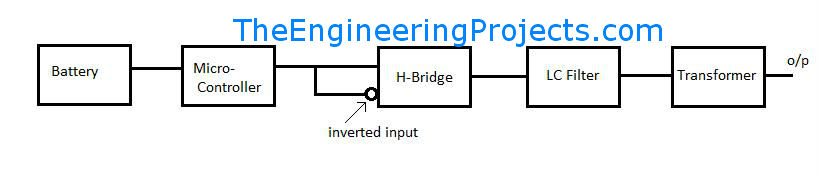
The exact order of filter and transformer depends on the topology. A filter placed on the low-voltage, high-current side requires a large-current inductor. A high-voltage-side filter carries less current but needs components rated for hazardous voltage. The feedback sensing point must match the voltage that the controller is expected to regulate.
Define the Electrical Requirements First
Before calculating PWM, define the input range, output voltage, output frequency, continuous VA, surge power, load power factor, allowable THD and isolation requirement. For a 230 V RMS sine wave:
Vpeak = Vrms × √2 = 230 V × 1.414 = 325.3 V
A transformer-fed 12 V bridge does not deliver 230 V merely because the turns ratio is 230:12. Semiconductor voltage drop, winding resistance, battery sag, modulation index and regulation margin all reduce the available voltage.
If a 300 W load is supplied from 12 V at 88% efficiency:
Iin = 300 W / (0.88 × 12 V) = 28.4 A
This average current does not include surge. The battery, fuse, conductors, switches and transformer primary must be designed for the actual worst case.
How SPWM Represents a Sine Wave
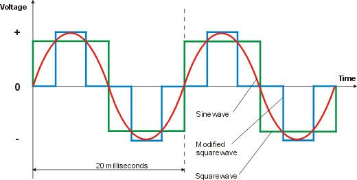
Sinusoidal pulse-width modulation keeps the power switches in on or off states while varying pulse width according to a sine reference. The switching waveform contains the required 50 Hz fundamental plus components clustered around the carrier frequency. A low-pass filter reduces the high-frequency content.
For sample number n in a table of N values, a normalized sine duty command is:
d[n] = 0.5 + 0.5 × M × sin(2πn/N)
M is the modulation index between zero and the linear limit of the selected scheme. An 8-bit timer represents duty commands from 0 to 255:
OCR[n] = round(255 × d[n])
A full-bridge implementation often uses the sign of the sine reference to select output polarity and its magnitude to set PWM duty. The gate driver then creates complementary high-side and low-side signals with guaranteed dead time.
Correct the AVR Carrier and Output Frequency
For an ATmega16 clocked at 8 MHz, Timer0 in 8-bit fast-PWM mode with no prescaler repeats every 256 clock cycles:
fPWM = FCPU / (prescaler × 256)
fPWM = 8,000,000 / (1 × 256) = 31,250 Hz
If firmware advances through one of 256 sine samples on every PWM overflow, the output frequency is:
fout = 31,250 / 256 = 122.07 Hz
That is not 50 Hz. We could reduce the update rate, change the carrier configuration or use a phase accumulator. A 32-bit phase accumulator gives accurate fractional stepping while keeping the 31.25 kHz carrier. Its increment is:
Phase increment = fout × 2³² / fPWM
Phase increment = 50 × 4,294,967,296 / 31,250 ≈ 6,871,948
Adding this number on every PWM overflow makes the upper eight accumulator bits cycle through a 256-entry table at approximately 50 Hz.
AVR SPWM Reference Code
The following AVR-GCC example demonstrates the corrected timing. The table named sine256 must contain 256 unsigned values generated from the duty equation. Store it in flash memory so it does not consume the ATmega16's limited SRAM.
#define F_CPU 8000000UL

#include <avr/io.h>
#include <avr/interrupt.h>
#include <avr/pgmspace.h>
#include <stdint.h>

#define PHASE_STEP_50HZ 6871948UL

/* Insert 256 values from 0 to 255 here.
   Each value is round(127.5 + 127.5*sin(2*pi*n/256)). */
const uint8_t sine256[256] PROGMEM = {
    /* 256 precomputed samples */
};

volatile uint32_t phaseAccumulator = 0;

static void pwm_init(void)
{
    DDRB |= (1 << PB3);       /* OC0 output */
    OCR0 = 128;

    /* Fast PWM, non-inverting OC0, timer clock = F_CPU */
    TCCR0 = (1 << WGM00) |
            (1 << WGM01) |
            (1 << COM01) |
            (1 << CS00);

    TIMSK |= (1 << TOIE0);
}

ISR(TIMER0_OVF_vect)
{
    uint8_t tableIndex;

    phaseAccumulator += PHASE_STEP_50HZ;
    tableIndex = (uint8_t)(phaseAccumulator >> 24);
    OCR0 = pgm_read_byte(&sine256[tableIndex]);
}

int main(void)
{
    pwm_init();
    sei();

    while (1) {
        /* Regulation, sensing and fault management belong here. */
    }
}
This program produces a single SPWM reference on OC0. After an appropriate low-pass filter, it can demonstrate a 50 Hz analog-shaped waveform centered within the logic supply. It is not a complete full-bridge controller because OC0 alone does not provide four interlocked gate signals, hardware dead time, polarity sequencing or a fault trip path.
For real bridge control, use a timer and gate driver that support complementary outputs and guaranteed dead time, or use a digital-power controller designed for this work. A hardware overcurrent signal should disable the PWM outputs without waiting for normal firmware.
Generating the Sine Table
The lookup table should be generated once on a development computer rather than calculated with floating-point trigonometry every time the small AVR starts. The value for index n is:
value[n] = round(127.5 + 127.5 × sin(2πn/256))
Check these properties before copying the table into firmware:
- There are exactly 256 entries.
- Every value is between 0 and 255.
- The average is close to 127.5.
- The samples cover one complete cycle without repeating the first point at the end.
- The generated fundamental frequency agrees with the phase-step calculation.
A table indexed from zero through 255 covers angles from zero up to slightly less than 360 degrees. Index 256 would begin the next cycle and is therefore not stored.
H-Bridge Circuit
The H-bridge is the power stage. Four controlled switches surround the load or transformer winding. The bridge does not amplify a waveform in the linear-amplifier sense; it switches the DC source into controlled voltage states.
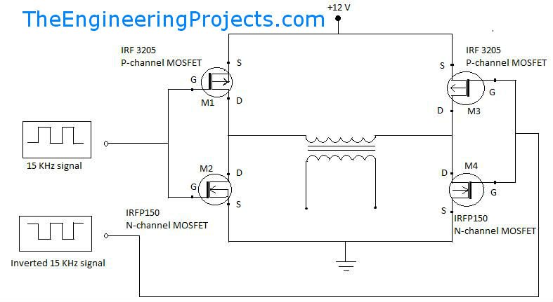
For a modern low-voltage bridge, four N-channel MOSFETs with suitable high-side and low-side gate drivers are often preferred because N-channel devices normally provide better conduction performance than comparable P-channel parts. A mixed P-channel and N-channel bridge can simplify high-side drive at low voltage, but it still requires dead time and proper gate control. Changing transistor polarity does not automatically prevent shoot-through.
Positive Output State
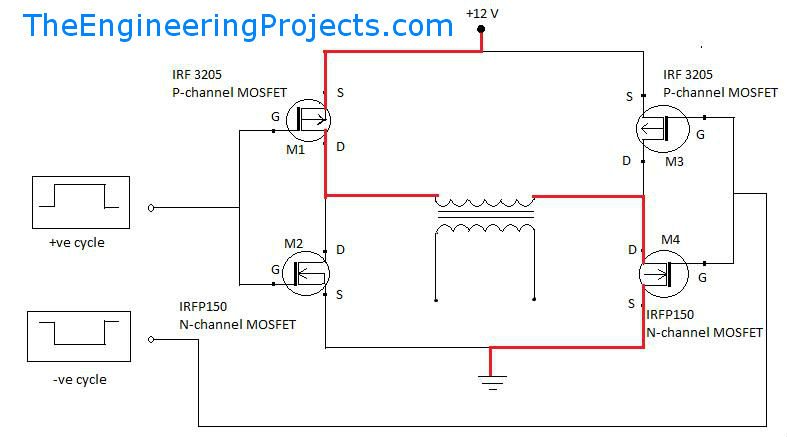
One diagonal pair conducts to apply positive DC-link voltage across the load. The other two commanded switches remain off. Current direction and freewheeling paths depend on load inductance and the active PWM state.
Negative Output State
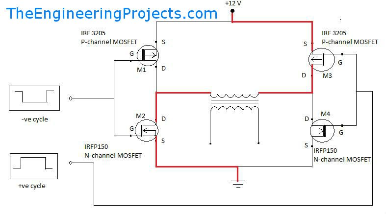
The opposite diagonal pair conducts to reverse the voltage. With a 12 V ideal DC link, the bridge can apply +12 V or -12 V, giving 24 V peak-to-peak. The useful RMS and fundamental values depend on modulation and filtering.
Dead Time and Shoot-Through
The upper and lower device in one bridge leg must never conduct together. If they do, they short the DC link. Dead time delays the turn-on of one device until its complement has turned off. It must cover driver propagation mismatch, MOSFET switching time, Miller coupling and worst-case temperature.
Do not use two general-purpose BC547 stages as the only protection between a microcontroller and a high-current bridge. Their delays are not a guaranteed dead-time mechanism. Use a gate driver with undervoltage lockout and interlocking, then verify the actual gate-source waveforms and bridge current.
Expected Bridge Waveform
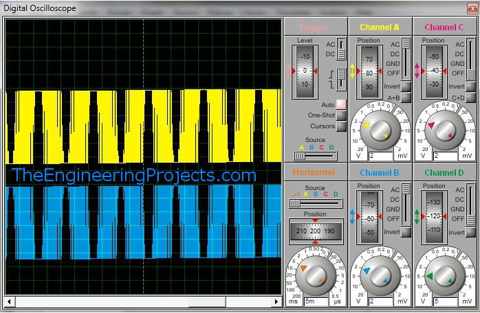
The unfiltered bridge output is a train of high-frequency pulses, not a smooth sine wave. Its duty envelope follows the 50 Hz reference. An oscilloscope's bandwidth, probe connection and math functions affect what you see. Never connect a grounded bench oscilloscope probe directly to a floating or mains-referenced bridge node unless the measurement method is rated and designed for that circuit.
LC Output Filter
An LC low-pass filter passes the 50 Hz fundamental while attenuating the 31.25 kHz carrier. A typical arrangement places the inductor in series and the capacitor across the output or load side.
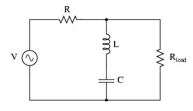
The ideal undamped resonant frequency is:
fc = 1 / (2π√(LC))
Suppose we begin with L = 3.3 mH and C = 1.0 µF:
fc = 1 / (2π√(0.0033 × 1.0 × 10^-6)) ≈ 2.77 kHz
This is well above 50 Hz and below 31.25 kHz, but it does not prove the filter is suitable. We must also evaluate attenuation, load range, damping, control-loop stability, inductor ripple and saturation current, capacitor RMS current and component voltage ratings.
A practical LC filter is not lossless. The inductor has winding and core loss, and the capacitor has ESR and dielectric loss. It is still normally more efficient than placing a large resistor in series with a power output.
Measure an Unknown Inductor by Resonance
The original project used resonance to estimate an unknown inductance because an LCR meter was unavailable. Connect the unknown inductor with a known capacitor in a low-energy test network driven through a current-limiting resistor.
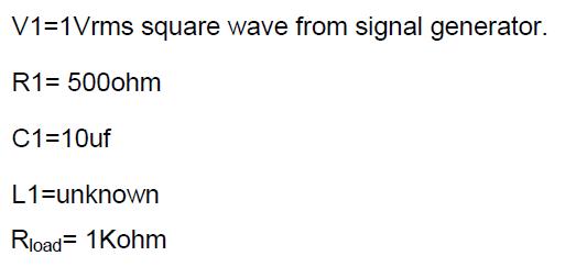
Adjust the function generator and identify the resonant frequency from the circuit response. For an ideal LC pair:
fr = 1 / (2π√(LC))
Rearranging for inductance gives:
L = 1 / (4π²fr²C)
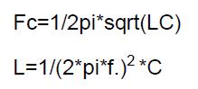
If a known 1.0 µF capacitor resonates at 2.00 kHz:
L = 1 / (4π² × (2000)² × 1.0 × 10^-6) = 6.33 mH
Capacitor tolerance, inductor resistance, core loss, generator impedance and measurement loading introduce error. Measure at a small signal that does not saturate or heat the core. An inductor measured at milliamperes may have lower inductance at the large current used in an inverter.
Transformer Stage
An ideal transformer follows:
Vs / Vp = Ns / Np
Vp × Ip = Vs × Is
A real inverter transformer needs margin for copper loss, flux density, temperature rise and battery sag. The applied bridge waveform must have balanced positive and negative volt-seconds. A DC offset can walk the core toward saturation and produce a destructive primary-current rise.
The transformer also does not remove all switching harmonics. Its leakage inductance and capacitance interact with the bridge and filter. The complete waveform and insulation performance must be verified on the intended hardware.
Closed-Loop Output Regulation
Open-loop SPWM produces an output that changes with battery voltage and load. A practical inverter measures output voltage, compares it with a reference and adjusts modulation index. The sensing circuit must provide the required galvanic isolation and bandwidth.
The feedback loop should regulate the fundamental or RMS output without chasing individual carrier pulses. Filter resonance adds phase shift, so compensation must be designed and tested over the intended load range. Limit the modulation command so a fault or controller windup cannot demand impossible duty cycles.
Protection Required Before Power Testing
| Protection | Reason |
|---|---|
| Battery-side fuse | Limits source energy during cable or bridge faults |
| Precharge or controlled connection | Limits DC-link capacitor inrush |
| Hardware overcurrent trip | Turns gates off within the safe response time |
| Gate-driver undervoltage lockout | Prevents partially enhanced MOSFETs |
| DC bus overvoltage and battery undervoltage limits | Protect capacitors, switches, battery and load |
| Overtemperature shutdown | Protects semiconductors and magnetics |
| Output short-circuit handling | Controls a severe load fault |
| Safe capacitor discharge | Reduces retained hazardous voltage after shutdown |
Recommended Bring-Up Sequence
- Run the PWM code in simulation and verify carrier and 50 Hz envelope mathematically.
- Observe OC0 through a logic analyzer or oscilloscope at logic-level energy only.
- Low-pass filter the reference signal and confirm its frequency, offset and shape.
- Test the gate driver with the DC power stage disconnected.
- Verify gate amplitude, dead time and default-off behavior.
- Power the bridge from a current-limited, isolated low-voltage source with a resistive test load.
- Measure current and temperature before adding the transformer and filter.
- Increase voltage and power only after current limiting and fault shutdown have been proven.
Common Design Problems
| Symptom | Probable cause | Engineering response |
|---|---|---|
| MOSFETs heat at no load | Shoot-through, slow gates or excessive switching loss | Measure both gate waveforms and bridge current; correct driver and dead time |
| High-side N-channel device stays off | Gate voltage is not above its moving source | Use a suitable bootstrap or isolated high-side driver |
| Output frequency is wrong | Sample rate and table length were confused | Calculate carrier, update rate and phase increment explicitly |
| Sine output is distorted under load | Open-loop voltage sag, filter saturation or insufficient bus voltage | Measure bus and inductor current; add correctly compensated feedback |
| Transformer current rises rapidly | Core saturation or DC volt-second imbalance | Stop immediately and correct timing, winding and flux design |
| Filter rings | High-Q LC resonance and inadequate damping | Model the load and control loop; add a designed damping network |
Practical Review
A sine-wave inverter does not apply an analog sine signal to MOSFET gates. It switches the devices fully on and off using PWM whose average follows a sine reference. The H-bridge supplies bipolar power, the LC network attenuates the carrier, and the transformer changes voltage where the topology requires it.
At 8 MHz, ATmega16 Timer0 fast PWM runs at 31.25 kHz without prescaling. A phase accumulator lets the code traverse a 256-entry sine table at 50 Hz without confusing carrier frequency, interrupt frequency and output frequency. That correct timing is only the waveform-generation layer; gate drive, dead time, feedback, protection, magnetics and thermal design complete the inverter.
Frequently Asked Questions
Why is the PWM carrier much higher than 50 Hz?
A high carrier lets pulse width represent many points along the 50 Hz sine reference and makes the switching components easier to separate with a filter. Higher frequency also raises switching loss, so it is a design tradeoff.
Can OC0 drive a MOSFET gate directly?
It should not drive a power bridge directly. Use a gate driver sized for the MOSFET charge and bus voltage. The driver must provide interlocking, dead time, high-side voltage and a fast fault shutdown path.
Why did 256 samples at each Timer0 overflow produce 122 Hz?
The overflow rate was 31,250 Hz. Dividing it by 256 samples per cycle gives 122.07 cycles per second. A phase accumulator advances through the table fractionally to obtain 50 Hz.
Can P-channel high-side MOSFETs eliminate shoot-through?
No. They may simplify level shifting in a low-voltage bridge, but incorrect overlap can still turn both devices in a leg on together. Dead time and reliable gate control remain necessary.
How do I choose the LC cutoff frequency?
Place it above the output fundamental and sufficiently below the switching carrier, then analyze attenuation, resonance, damping, component current, load range and feedback stability. The resonance formula provides a starting point only.
Why is the sine table stored in flash?
The ATmega16 has limited SRAM. A constant 256-byte table does not need writable memory, so program memory is a better location.
Does the transformer guarantee a clean sine output?
No. Waveform quality depends on modulation, switching timing, filter design, transformer behavior, bus voltage and feedback. A transformer changes voltage and may provide isolation, but it is not a complete harmonic filter.
Can I connect this experimental design to household wiring?
No. Mains-level inverter work can cause fatal shock or fire, and grid connection requires certified synchronization and anti-islanding protection. Use an isolated, current-limited laboratory setup and qualified hardware practices.